

Page 1
®
For most current data sheet and other product
information, visit www.burr-brown.com
Programmable Gain
DIFFERENCE AMPLIFIER
INA145
INA145
FEATURES
● DIFFERENTIAL GAIN = 1V/V TO 1000V/V:
Set with External Resistors
● LOW QUIESCENT CURRENT: 570µA
● WIDE SUPPLY RANGE:
Single Supply: 4.5V to 36V
Dual Supplies: ±2.25V to ±18V
● HIGH COMMON-MODE VOLTAGE:
+8V at VS = +5V
±28V at V
= ±15V
S
● LOW GAIN ERROR: 0.01%
● HIGH CMR: 86dB
● SO-8 PACKAGE
APPLICATIONS
● CURRENT SHUNT MEASUREMENTS
● SENSOR AMPLIFIER
●
DIFFERENTIAL LINE RECEIVER
● BATTERY POWERED SYSTEMS
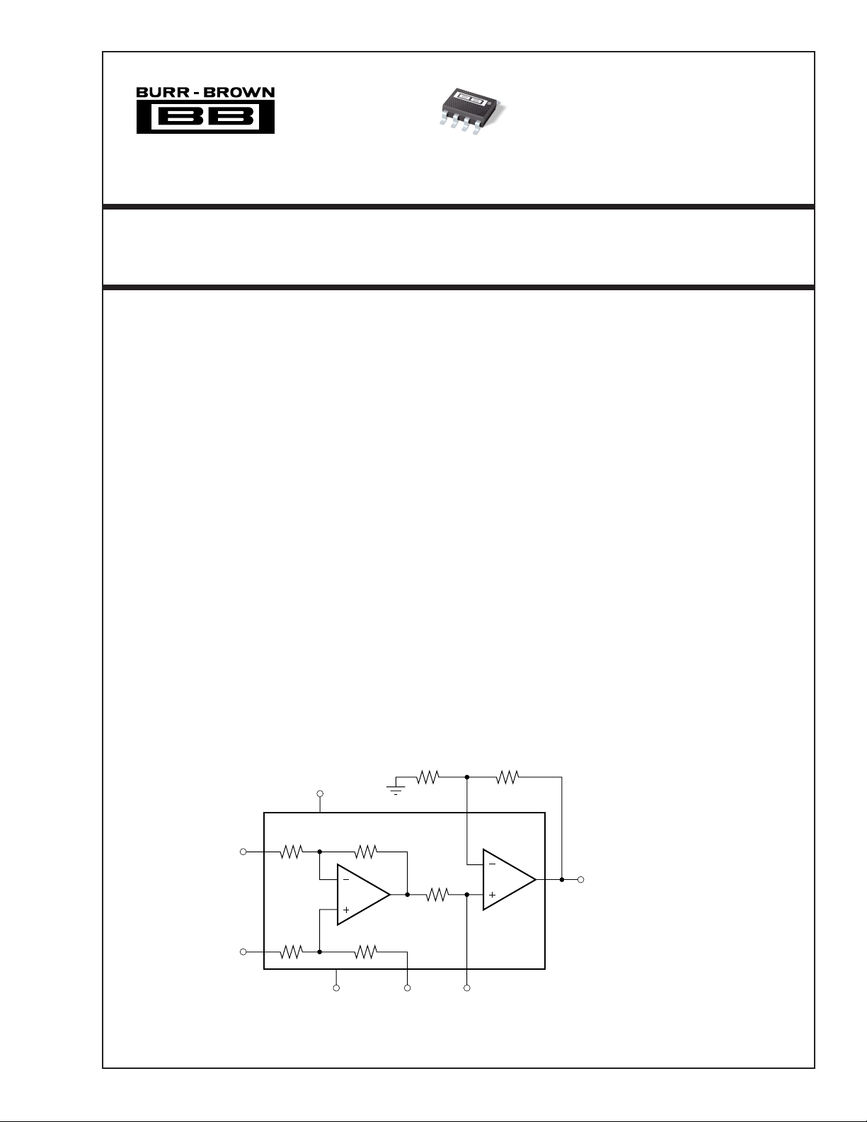
DESCRIPTION
The INA145 is a precision, unity-gain difference
amplifier consisting of a precision op amp and onchip precision resistor network. Two external resistors
set the gain from 1V/V to 1000V/V. The input common-mode voltage range extends beyond the positive
and negative rails.
On-chip precision resistors are laser-trimmed to achieve
accurate gain and high common-mode rejection. Excellent TCR tracking of these resistors assures continued high precision over temperature.
The INA145 is available in the SO-8 surface-mount
package specified for the extended industrial temperature range, –40°C to +85°C.
SBOS120
R
G1
V+
R
10kΩ
(1%)
R
5
1
7
R
1
40kΩ
2
–
V
IN
G = 1
R
3
40kΩ
3
+
V
IN
International Airport Industrial Park • Mailing Address: PO Box 11400, Tucson, AZ 85734 • Street Address: 6730 S. Tucson Blvd., Tucson, AZ 85706 • Tel: (520) 746-1111
Twx: 910-952-1111 • Internet: http://www.burr-brown.com/ • Cable: BBRCORP • Telex: 066-6491 • FAX: (520) 889-1510 • Immediate Product Info: (800) 548-6132
R
2
40kΩ
A1
R
4
40kΩ
418
RefV–
©1999 Burr-Brown Corporation PDS-1567B Printed in U.S.A. March, 2000
R
G2
G
5
A2
INA145
V
01
V
6
O
+–
V
= (VIN – VIN)(1 + RG2/RG1)
O
INA145
®
Page 2

SPECIFICATIONS: VS = ±2.25V to ±18V
Boldface limits apply over the specified temperature range, TA = –40°C to +85°C
At TA = +25°C, G = 1, RL = 10kΩ connected to ground and ref pin connected to ground unless otherwise noted.
INA145UA
PARAMETER CONDITION MIN TYP MAX UNITS
OFFSET VOLTAGE, V
Input Offset Voltage V
vs Temperature ∆V
vs Power Supply PSRR V
O
OS
/∆T See Typical Curve
OS
vs Time ±0.3 µV/mo
Offset Voltage, V
01
INPUT VOLTAGE RANGE
Common-Mode Voltage Range V
Common-Mode Rejection CMRR V
CM
Over Temperature V
INPUT BIAS CURRENT
Bias Current I
Offset Current I
(2)
B
OS
(VIN+) – (VIN–) = 0V, VO = 0V 2(V–) 2(V+) –2 V
= 2(V–) to 2(V+) – 2V, RS = 0Ω 76 86 dB
CM
INPUT IMPEDANCE
Differential (non-inverting input) 80 kΩ
Differential (inverting input) 27 kΩ
Common-Mode 40 kΩ
NOISE RTI
Voltage Noise, f = 0.1Hz to 10Hz 2 µVp-p
Voltage Noise Density, f = 1kHz e
n
GAIN
Gain Equation G = 1 + RG2/R
(1)
Initial
Gain Error R
vs Temperature R
vs Temperature R
Nonlinearity R
= 100kΩ, VO = (V–)+0.15 to (V+)–1, G = 1 ±0.01 ±0.1 %
L
= 100kΩ, VO = (V–)+0.25 to (V+)–1, G = 1 ±2 ±10 ppm/°C
L
= 10kΩ, VO = (V–)+0.3 to (V+)–1.25, G = 1 ±0.01 ±0.1 %
R
L
= 10kΩ, VO = (V–)+0.5 to (V+)–1.25, G = 1 ±2 ±10 ppm/°C
L
= 10kΩ, VO = (V–)+0.3 to (V+)–1.25, G = 1 ±0.0002 ±0.005 % of FS
L
FREQUENCY RESPONSE
Small Signal Bandwidth G = 1 500 kHz
Slew Rate 0.45 V/µs
Settling Time, 0.1% G = 1, 10V Step 40 µs
0.01% G = 1, 10V Step 90 µs
Overload Recovery 50% Input Overload 40 µs
OUTPUT, V
Voltage Output RL = 100kΩ, G = 1 (V–) + 0.15 (V+) – 1 V
O
Over Temperature R
Over Temperature R
Short-Circuit Current Continuous to Common ±15 mA
Capacitive Load Stable Operation 1000 pF
POWER SUPPLY
Specified Voltage Range, Dual Supplies ±2.25 ±18 V
Operating Voltage Range ±1.35 ±18 V
Quiescent Current V
Over Temperature
TEMPERATURE RANGE
Specified Range –40 +85 °C
Operating Range –55 +125 °C
Storage Range –55 +125 °C
Thermal Resistance
θ
JA
NOTES: (1) Referred to input pins (VIN+ and VIN–), Gain = 1V/V. Specified with 10kΩ in feedback of A2. (2) Input offset voltage specification includes effects of amplifier’s
input bias and offset currents. (3) Includes effects of input bias current noise and thermal noise contribution of resistor network.
(1, 2)
RTI
V
= VO = 0V ±0.2 ±1mV
CM
= ±1.35V to ±18V ±20 ±60 µV/V
S
(1, 2)
RTI
= ±15V 70 80 dB
S
±0.4 mV
VCM = VS/2
±50 nA
±5nA
(1, 3)
90 nV/√Hz
G = 1 to 1000
G1
1V/V
V/V
G = 10 50 kHz
= 100kΩ, G = 1 (V–) + 0.25 (V+) – 1 V
L
= 10kΩ, G = 1 (V–) + 0.3 (V+) – 1.25 V
R
L
= 10kΩ, G = 1 (V–) + 0.5 (V+) – 1.25 V
L
= 0, IO = 0 ±570 ±700 µA
IN
±800 µA
150 °C/W
The information provided herein is believed to be reliable; however, BURR-BROWN assumes no responsibility for inaccuracies or omissions. BURR-BROWN assumes
no responsibility for the use of this information, and all use of such information shall be entirely at the user’s own risk. Prices and specifications are subject to change
without notice. No patent rights or licenses to any of the circuits described herein are implied or granted to any third party. BURR-BROWN does not authorize or warrant
any BURR-BROWN product for use in life support devices and/or systems.
®
INA145
2
Page 3
SPECIFICATIONS: VS = +5V Single Supply
Boldface limits apply over the specified temperature range, TA = –40°C to +85°C
At TA = +25°C, G = 1, RL = 10kΩ connected to ground and ref pin connected to 2.5V unless otherwise noted.
INA145UA
PARAMETER CONDITION MIN TYP MAX UNITS
OFFSET VOLTAGE, V
Input Offset Voltage V
vs Temperature ∆V
vs Power Supply Rejection Ratio PSRR V
O
OS
/∆T See Typical Curve
OS
vs Time ±0.3 µV/mo
Offset Voltage, V
INPUT VOLTAGE RANGE
Common-Mode Voltage Range
Common-Mode Rejection Ratio CMRR V
Over Temperature 80 dB
INPUT BIAS CURRENT
Bias Current I
Offset Current I
01
(3)
(2)
V
CM
B
OS
VIN+ – VIN– = 0V, VO = 2.5V –2.5 5.5 V
= –2.5V to +5.5V, RS = 0Ω 76 86 dB
CM
INPUT IMPEDANCE
Differential (non-inverting input) 80 kΩ
Differential (inverting input) 27 kΩ
Common-Mode 40 kΩ
NOISE RTI
Voltage Noise, f = 0.1Hz to 10Hz 2 µVp-p
Voltage Noise Density, f = 1kHz e
n
GAIN
Gain Equation G = 1 + R
(1)
Initial
Gain Error R
vs Temperature R
vs Temperature R
Nonlinearity R
= 100kΩ, VO = 0.15V to 4V, G = 1 ±0.01 ±0.1 %
L
= 100kΩ, VO = 0.25V to 4V, G = 1 ±2 ±10 ppm/°C
L
= 10kΩ, VO = 0.3V to 3.75V, G = 1 ±0.01 ±0.1 %
R
L
= 10kΩ, VO = 0.5V to 3.75V, G = 1 ±2 ±10 ppm/°C
L
= 10kΩ, VO = +0.3 to +3.75, G = 1 ±0.001 ±0.005 % of FS
L
FREQUENCY RESPONSE
Small Signal Bandwidth G = 0.1 500 kHz
Slew Rate 0.45 V/µs
Settling Time, 0.1% G = 1, 10V Step 40 µs
0.01% G = 1, 10V Step 90 µs
Overload Recovery 50% Input Overload 40 µs
OUTPUT, V
Voltage Output RL = 100kΩ, G = 1 0.15 4 V
O
Over Temperature R
Over Temperature R
Short-Circuit Current Continuous to Common ±15 mA
Capacitive Load Stable Operation 1000 pF
POWER SUPPLY
Specified Voltage Range, Single Supply +4.5 +36 V
Operating Voltage Range +2.7 +36 V
Quiescent Current V
Over Temperature 800 µA
TEMPERATURE RANGE
Specified Range –40 +85 °C
Operating Range –55 +125 °C
Storage Range –55 +125 °C
Thermal Resistance
NOTES: (1) Referred to input pins (V
amplifier’s input bias and offset currents. (3) Common-mode voltage range with single supply is 2(V+) – 2V – V
θ
JA
+ and VIN–), Gain = 1V/V. Specified with 10kΩ in feedback of A2. (2) Input offset voltage specification includes effects of
IN
noise and thermal noise contribution of resistor network.
(1, 2)
RTI
V
= VO = 2.5V ±0.35 ±1mV
CM
= ±1.35V to ±18V ±20 ±60 µV/°C
S
(1, 2)
RTI
±0.55 mV
±50 nA
±5nA
(1, 4)
90 nV/√Hz
G = 1 to 1000
G2/RG1
1V/V
G = 1 50 kHz
= 100kΩ, G = 1 0.25 4 V
L
= 10kΩ, G = 1 0.3 3.75 V
R
L
= 10kΩ, G = 1 0.5 3.75 V
L
= 0, IO = 0 550 700 µA
IN
150 °C/W
to –V
REF
. (4) Includes effects of input current
REF
V/V
V/V
®
3
INA145
Page 4
AMPLIFIER A1, A2 PERFORMANCE
Boldface limits apply over the specified temperature range, TA = –40°C to +85°C
At TA = +25°C, G = 1, RL = 10kΩ connected to ground and ref pin connected to ground unless otherwise noted.
INA145UA
PARAMETER CONDITION MIN TYP MAX UNITS
OFFSET VOLTAGE, V
Input Offset Voltage V
vs Temperature ∆V
INPUT VOLTAGE RANGE
Common-Mode Voltage Range V
Common-Mode Rejection Ratio CMRR V
OPEN-LOOP GAIN
Open Loop Gain A
INPUT BIAS CURRENT
Bias Current I
Offset Current I
RESISTOR AT A1 OUTPUT, V
Initial 10 kΩ
Error ±0.2 %
Temperature Drift Coefficient ±50 ppm/°C
O
(2)
O1
OS
/∆T ±1 µV/°C
OS
CM
OL
B
OS
VS = ±15V, V
VIN+ – VIN– = 0V, VO = 0V (V–) to (V+) –1 V
(1, 2)
RTI
= VO = 0V ±0.5 mV
CM
= (V–) to (V+) –1 90 dB
CM
110 dB
±50 nA
±5nA
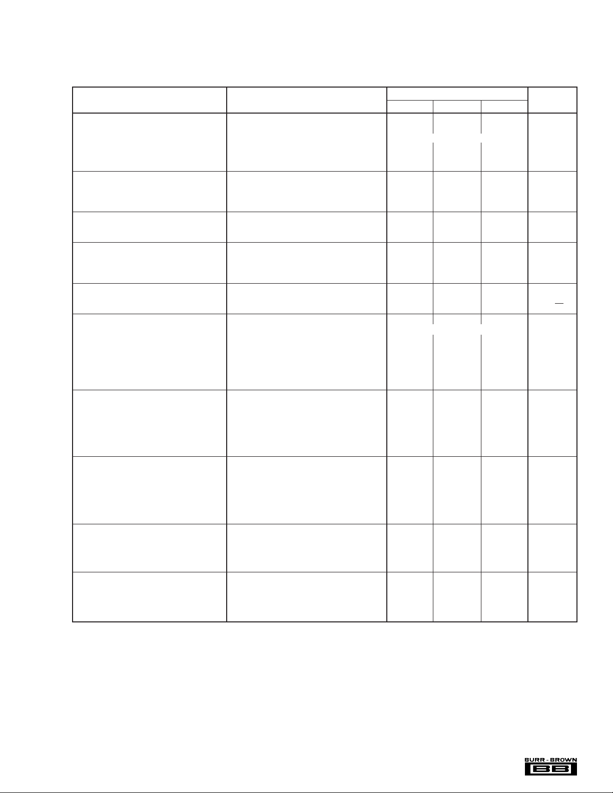
PIN CONFIGURATION
Top View SO-8
1
Ref
–
2
V
IN
+
3
V
IN
4
V–
ABSOLUTE MAXIMUM RATINGS
Supply Voltage, V+ to V–.................................................................... 36V
Signal Input Terminals, Voltage ........................................................ ±80V
Output Short Circuit (to ground) .............................................. Continuous
Operating Temperature ..................................................–55°C to +125°C
Storage Temperature ..................................................... –55°C to +150°C
Junction Temperature .................................................................... +150°C
Lead Temperature (soldering, 10s) ............................................... +240°C
NOTE: (1) Stresses above these ratings may cause permanent damage.
Exposure to absolute maximum conditions for extended periods may degrade
device reliability.
Current .......................................................±1mA
8
V
O1
7
V+
6
V
O
5
R
G
(1)
ELECTROSTATIC
DISCHARGE SENSITIVITY
This integrated circuit can be damaged by ESD. Burr-Brown
recommends that all integrated circuits be handled with
appropriate precautions. Failure to observe proper handling
and installation procedures can cause damage.
ESD damage can range from subtle performance degradation
to complete device failure. Precision integrated circuits may
be more susceptible to damage because very small parametric
changes could cause the device not to meet its published
specifications.
PACKAGE/ORDERING INFORMATION
PACKAGE SPECIFIED
PRODUCT PACKAGE NUMBER RANGE MARKING NUMBER
INA145UA SO-8 182 –40°C to +85°C INA145UA INA145UA Rails
DRAWING TEMPERATURE PACKAGE ORDERING TRANSPORT
"""""INA145UA/2K5 Tape and Reel
NOTE: (1) Models with a slash (/) are available only in Tape and Reel in the quantities indicated (e.g., /2K5 indicates 2500 devices per reel). Ordering 2500 pieces
of “INA145UA/2K5” will get a single 2500-piece Tape and Reel.
®
INA145
4
(1)
MEDIA
Page 5
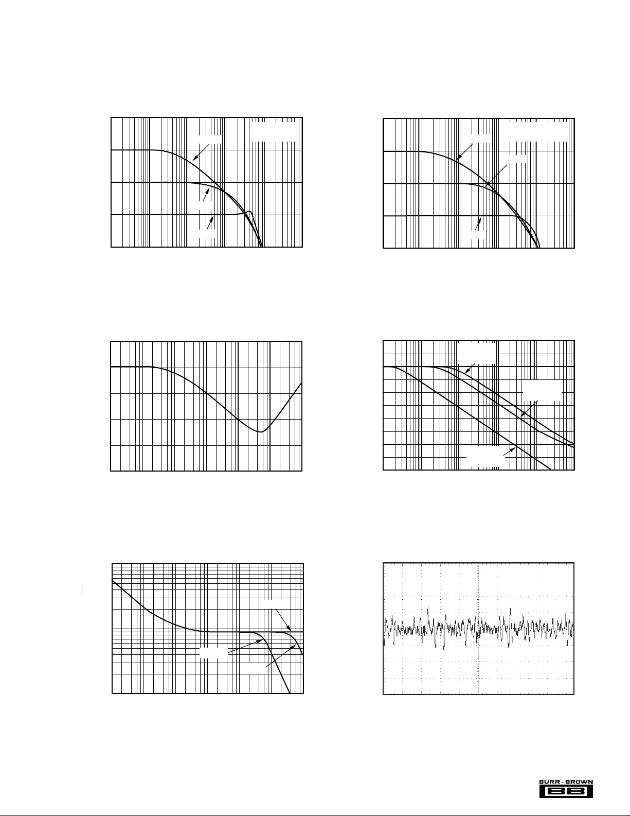
TYPICAL PERFORMANCE CURVES
GAIN vs FREQUENCY
Frequency (Hz)
Voltage Gain (dB)
100 1K 10K 1M 10M
60
40
20
0
–20
100K
G = 100
G = 10
G = 1
VS = ±15V
C
L
= 200pF 10kΩ
At TA = +25°C, VS = ±15V, G = 1, RL = 10kΩ connected to ground and Ref pin connected to ground, unless otherwise noted.
60
40
20
Voltage Gain (dB)
0
–20
100 1K 10K 1M 10M
100
80
60
COMMON-MODE REJECTION vs FREQUENCY
GAIN vs FREQUENCY
G = 100
G = 10
G = 1
100K
Frequency (Hz)
VS = ±15V
C
= 1000pF
L
100
POWER SUPPLY REJECTION vs FREQUENCY
PSR+
= ±15V)
(V
80
60
S
PSR+
= +5V)
(V
S
40
20
Common-Mode Rejection (dB)
0
10 100 1k 1M 10M
1k
100
Input Voltage Noise (nV/√Hz
10
0.1 1 10 10k 100k
INPUT VOLTAGE NOISE DENSITY
10k 100k
Frequency (Hz)
G = 1
G = 100
G = 10
100 1k
Frequency (Hz)
40
20
Power Supply Rejection (dB)
0
1 10 100 10k 100k
0.1Hz to 10Hz VOLTAGE NOISE (RTI)
500nV/div
PSR–
= ±15V)
(V
S
1k
Frequency (Hz)
500ms/div
®
5
INA145
Page 6

TYPICAL PERFORMANCE CURVES (Cont.)
At TA = +25°C, VS = ±15V, G = 1, RL = 10kΩ connected to ground and Ref pin connected to ground, unless otherwise noted.
670
650
630
610
590
570
(µA)
Q
I
550
530
510
490
470
110
100
Open-Loop Gain (dB)
–10
SHORT-CIRCUIT CURRENT vs TEMPERATURE
–60 –40 0–20 80 100
90
80
70
60
50
40
30
20
10
0
1 10 100 100k 1M
QUIESCENT CURRENT AND
I
SC
I
Q
20
Temperature (°C)
GAIN AND PHASE vs FREQUENCY
Op Amp A1 and A2
G
Frequency (Hz)
6040
RL = 10kΩ || 200pF
Φ
RL = 1nF
1k 10k
G = 1
120
140
20
18
16
14
12
10
8
6
4
2
0
–90
–135
–180
(mA)
SC
I
0.6
G = 1
0.55
0.5
0.45
0.4
0.35
Sew Rate (V/µs)
0.3
0.25
0.2
–60 –40 0–20 80 100
160
140
120
100
80
Phase (°)
60
Settling Time (µs)
40
20
0
1 100
SLEW RATE vs TEMPERATURE
G = 1
0.01%
G = 1
0.1%
10
6040
G = 10
0.01%
G = 10
0.1%
20
Temperature (°C)
SETTLING TIME vs LOAD CAPACITANCE
Load Capacitance (nF)
120
140
MAXIMUM OUTPUT VOLTAGE SWING
15
10
5
0
–5
Output Voltage Swing (V)
–10
–15
0246810121416
®
vs OUTPUT CURRENT
+125°C
+85°C
–55°C
–55°C
+125°C
–25°C
Output Current (mA)
+85°C
INA145
–25°C
+25°C
+25°C
OFFSET VOLTAGE
PRODUCTION DISTRIBUTION
= ±2.25V
V
S
Relative Frequency
–1
–0.8
–0.6
–0.4
Offset Voltage, RTI (mV)
0
–0.2
Typical Production
Distribution of
Packaged Units.
0.2
0.4
0.6
0.8
1
6
Page 7

TYPICAL PERFORMANCE CURVES (Cont.)
OFFSET VOLTAGE DRIFT
PRODUCTION DISTRIBUTION
Offset Voltage Drift, RTI (µV/°C)
–10
–9–8–7–6–5–4–3–2–1
012345678
9
10
20
15
10
5
0
VS = ±15V
Relative Frequency
At TA = +25°C, VS = ±15V, G = 1, RL = 10kΩ connected to ground and Ref pin connected to ground, unless otherwise noted.
OFFSET VOLTAGE
PRODUCTION DISTRIBUTION
VS = ±15V
Relative Frequency
Typical Production
Distribution of
Packaged Devices
–1
50mV/div
0
–0.8
–0.6
–0.4
–0.2
Offset Voltage, RTI (mV)
SMALL-SIGNAL STEP RESPONSE
(G = 1, R
SMALL-SIGNAL STEP RESPONSE
= 10kΩ, CL = 200pF)
L
5µs/div
(G = 10, C
= 1000pF)
L
0.2
0.4
0.6
0.8
1
SMALL-SIGNAL STEP RESPONSE
(G = 1, C
50mV/div
LARGE-SIGNAL STEP RESPONSE
(G = 10, R
= 1000pF)
L
5µs/div
= 10kΩ, CL = 200pF)
L
50mV/div
5µs/div
5V/div
50µs/div
®
7
INA145
Page 8

APPLICATION INFORMATION
The INA145 is a programmable gain difference amplifier
consisting of a gain of 1 difference amplifier and a programmable-gain output buffer stage. Basic circuit connections are
shown in Figure 1. Power supply bypass capacitors should
be connected close to pins 4 and 7, as shown. The amplifier
is programmable in the range of G = 1 to G = 1000 with two
external resistors.
The output of A1 is connected to the noninverting input of
A2 through a 10kΩ resistor which is trimmed to ±1%
absolute accuracy. The A2 input is available for applications
such as a filter or a precision current source. See application
figures for examples.
SETTING THE GAIN
The gain of the INA145 is set by using two external
resistors, RG1 and RG2, according to the equation:
G = 1 + RG2/R
G1
For a total gain of 1, A2 is connected as a buffer amplifier
with no RG1. A feedback resistor, RG2 = 10kΩ, should be
used in the buffer connection. This provides bias current
cancellation (in combination with internal R5) to assure
specified offset voltage performance. Commonly used values are shown in the table of Figure 1. Resistor values for
other gains should be chosen to provide a 10kΩ parallel
resistance.
OPERATING VOLTAGE
The INA145 is fully specified for supply voltages from
±2.25V to ±18V, with key parameters guaranteed over the
temperature range –40°C to +85°C. The INA145 can be
operated with single or dual supplies, with excellent performance. Parameters that vary significantly with operating
voltage, load conditions, or temperature are shown in the
typical performance curves.
+V
S
0.1µF
7
R
1
–
V
IN
40kΩ
2
R
40kΩ
A1
2
R
G1
10kΩ
(1%)
R
G2
R
B
5
R
5
A2
COMMON-MODE RANGE
The input resistors of the INA145 provides an input common-mode range that extends well beyond the power supply
rails. Exact range depends on the power supply voltage and
the voltage applied to the Ref terminal (pin 1). To assure
proper operation, the voltage at the non-inverting input of
A1 (an internal node) must be within its linear operating
range. Its voltage is determined by the simple 1:1 voltage
divider between pin 3 and pin 1. This voltage must be
between V– and (V+) – 1V.
+–
VO = (VIN – VIN)(1 + RG2/RG1)
V
O
6
R
3
+
V
IN
40kΩ
3
0.1µF
R
4
40kΩ
418
–V
S
FIGURE 1. Basic Circuit Connections.
®
INA145
STANDARD 1% RESISTORS
TOTAL GAIN
(V/V) (V/V) (W) (W) (W)
INA145
V
01
1 1 (None) 10k —
2 2 20k 20k —
5 5 12.4k 49.9k —
10 10 11.0k 100k —
20 20 10.5k 200k —
50 50 10.2k 499k —
100 100 10.2k 1M —
200 200 499 100k 9.53k
500 500 100 49.9k 10k
1000 1000 100 100k 10k
A2 GAIN
R
R
G1
G2
R
B
8
Page 9
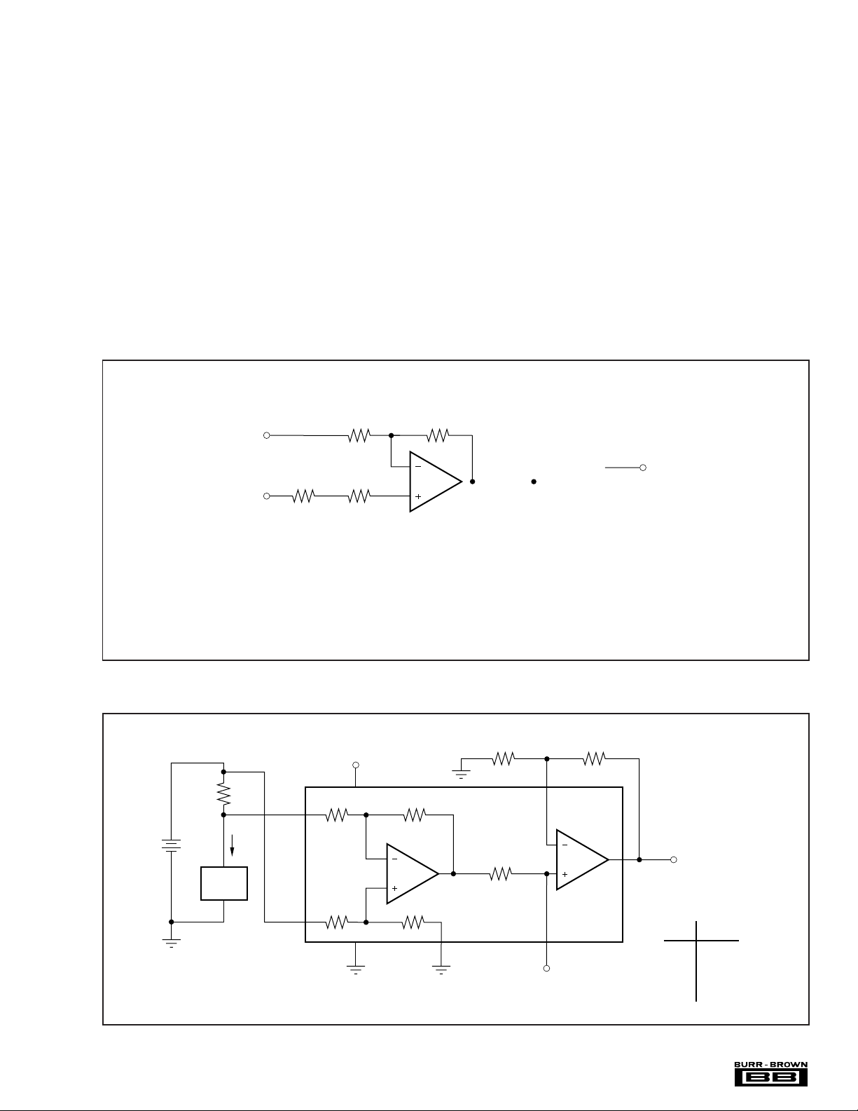
OFFSET TRIM
The INA145 is laser-trimmed for low offset voltage and
drift. Most applications require no external offset adjustment. Figure 2 shows an optional circuit for trimming the
offset voltage. A voltage applied to the Ref terminal will
be summed with the output signal. This can be used to null
offset voltage. To maintain good common-mode rejection,
the source impedance of a signal applied to the Ref
terminal should be less than 10Ω and a resistor added to
the positive input terminal should be 10 times that, or
100Ω. Alternatively, the trim voltage can be buffered with
an op amp such as the OPA277.
V
IN
INPUT IMPEDANCE
The input impedance of the INA145 is determined by the
input resistor network and is approximately 40kΩ. The
source impedance at the two input terminals must be nearly
equal to maintain good common-mode rejection. A 5Ω
mismatch in impedance between the two inputs will cause
the typical common-mode rejection to be degraded to approximately 72dB. Figure 7 shows a common application
measuring power supply current through a shunt resistor.
The source impedance of the shunt resistor, RS, is balanced
by an equal compensation resistor, RC.
Source impedances greater than 300Ω are not recommended,
even if they are perfectly matched. Internal resistors are laser
trimmed for accurate ratios, not to absolute values. Adding
equal resistors greater than 300Ω can cause a mismatch in
the total resistor ratios, degrading CMR.
10kΩ
10Ω
V
IN
Offset Adjustment Range = ±15mV, RTI ±
FIGURE 2. Optional Offset Trim Circuit.
R
S
1Ω
Load
I
L
V
B
2
V+
+5V
V
A1
1
R
G1
10.2kΩ
7
10kΩ
R
G2
1MΩ
5
O
G = 100
VO = 100 ILR
6
S
3
FIGURE 3. Measuring Current with Shunt Resistor.
INA145
14
8
9
V+ Max V
+5V 8V
+7V 12V
+10V 18V
+15V 28V
INA145
B
®
Page 10

Pole at
106Hz
R
G1
10kΩ
G = 1
1500pF
R
G2
1MΩ
10kΩ
5
–
2
V
IN
2
–
V
IN
+
3
V
IN
FIGURE 4. Noise Filtering.
R
–
2
V
IN
3
+
V
IN
1
R
3
5
10kΩ
INA145
18
22nF
R
2
R
4
1
Pole at
720Hz
10kΩ
6
V
O
3
+
V
O
6
V
IN
INA145
81
R
3
G =
R
R
3
R
+ R
3
4
4
G ≤ 1
FIGURE 5. Creating Gains Less Than Unity.
R
G2
10kΩ
5
0V ≤ VO ≤ 5V
V
6
O
INA145
8
1N914
Alternate
Soft Clamp
To Pin 8
1N4684
(3.3V)
Voltage
Reference
NOTE: (1) 1/2 OPA2342 with V
FIGURE 6. Clamp Circuits.
®
INA145
5.0V
or Analog-to-Digital V
connected to +5V and GND.
S
S
1N914
(1)
1N914
(1)
10
Page 11

R
V
O
I
OUT
= (VIN – VIN)/10kΩ
1
8
6
R
G2
10kΩ
10kΩ
INA145
5
2
3
V
IN
–+
V
IN
+
–
G1
11kΩ
R
G2
100kΩ
For sense resistors (RS)
greater than 5Ω, use
series compensation
resistor (R
common-mode rejection.
) for good
C
Sense resistors greater
than 200Ω are not
recommended.
FIGURE 7. Current Monitor, G = 1.
24V
2
SHUNT
R-I Lamp/10
e.g., 0.1Ω for 1A
3
Power
Supply
Load
R
10Ω
R
10Ω
2
C
S
3
57
148
Feedback
INA145
10MΩ
18
8.4kΩ
V
O
6
1V – 50mV
5
G = 10
V
O
6
INA145
V
O1
+5V
8kΩ
1V
10kΩ
2kΩ
Lamp
FIGURE 8. Comparator Output with Optional Hysteresis Application to Sense Lamp Burn-Out.
R
G1
11kΩ
–
2
V
IN
3
+
V
IN
Pole at
f = = 1.6Hz
2πR
18
1
1RC
R
G2
100kΩ
5
6
V
O
R
1
1MΩ
INA145
C
1
0.1µF
OPA277
FIGURE 9. AC Coupling (DC Restoration). FIGURE 10. Precision Current Source.
®
11
INA145
Page 12

PACKAGE OPTION ADDENDUM
www.ti.com
22-Oct-2007
PACKAGING INFORMATION
Orderable Device Status
(1)
Package
Type
Package
Drawing
Pins Package
Qty
Eco Plan
INA145UA ACTIVE SOIC D 8 100 Green (RoHS &
no Sb/Br)
INA145UA/2K5 ACTIVE SOIC D 8 2500 Green (RoHS &
no Sb/Br)
INA145UA/2K5E4 ACTIVE SOIC D 8 2500 Green (RoHS &
no Sb/Br)
INA145UAE4 ACTIVE SOIC D 8 100 Green (RoHS &
no Sb/Br)
(1)
The marketing status values are defined as follows:
ACTIVE: Product device recommended for new designs.
LIFEBUY: TI has announced that the device will be discontinued, and a lifetime-buy period is in effect.
NRND: Not recommended for new designs. Device is in production to support existing customers, but TI does not recommend using this part in
a new design.
PREVIEW: Device has been announced but is not in production. Samples may or may not be available.
OBSOLETE: TI has discontinued the production of the device.
(2)
Eco Plan - The planned eco-friendly classification: Pb-Free (RoHS), Pb-Free (RoHS Exempt), or Green (RoHS & no Sb/Br) - please check
http://www.ti.com/productcontent for the latest availability information and additional product content details.
TBD: The Pb-Free/Green conversion plan has not been defined.
Pb-Free (RoHS): TI's terms "Lead-Free" or "Pb-Free" mean semiconductor products that are compatible with the current RoHS requirements
for all 6 substances, including the requirement that lead not exceed 0.1% by weight in homogeneous materials. Where designed to be soldered
at high temperatures, TI Pb-Free products are suitable for use in specified lead-free processes.
Pb-Free (RoHS Exempt): This component has a RoHS exemption for either 1) lead-based flip-chip solder bumps used between the die and
package, or 2) lead-based die adhesive used between the die and leadframe. The component is otherwise considered Pb-Free (RoHS
compatible) as defined above.
Green (RoHS & no Sb/Br): TI defines "Green" to mean Pb-Free (RoHS compatible), and free of Bromine (Br) and Antimony (Sb) based flame
retardants (Br or Sb do not exceed 0.1% by weight in homogeneous material)
(2)
Lead/Ball Finish MSL Peak Temp
CU NIPDAU Level-3-260C-168 HR
CU NIPDAU Level-3-260C-168 HR
CU NIPDAU Level-3-260C-168 HR
CU NIPDAU Level-3-260C-168 HR
(3)
(3)
MSL, Peak Temp. -- The Moisture Sensitivity Level rating according to the JEDEC industry standard classifications, and peak solder
temperature.
Important Information and Disclaimer:The information provided on this page represents TI's knowledge and belief as of the date that it is
provided. TI bases its knowledge and belief on information provided by third parties, and makes no representation or warranty as to the
accuracy of such information. Efforts are underway to better integrate information from third parties. TI has taken and continues to take
reasonable steps to provide representative and accurate information but may not have conducted destructive testing or chemical analysis on
incoming materials and chemicals. TI and TI suppliers consider certain information to be proprietary, and thus CAS numbers and other limited
information may not be available for release.
In no event shall TI's liability arising out of such information exceed the total purchase price of the TI part(s) at issue in this document sold by TI
to Customer on an annual basis.
Addendum-Page 1
Page 13

PACKAGE MATERIALS INFORMATION
www.ti.com
TAPE AND REEL INFORMATION
11-Mar-2008
*All dimensions are nominal
Device Package
INA145UA/2K5 SOIC D 8 2500 330.0 12.4 6.4 5.2 2.1 8.0 12.0 Q1
Type
Package
Drawing
Pins SPQ Reel
Diameter
(mm)
Reel
Width
W1 (mm)
A0 (mm) B0 (mm) K0 (mm) P1
(mm)W(mm)
Pin1
Quadrant
Pack Materials-Page 1
Page 14

PACKAGE MATERIALS INFORMATION
www.ti.com
11-Mar-2008
*All dimensions are nominal
Device Package Type Package Drawing Pins SPQ Length (mm) Width (mm) Height (mm)
INA145UA/2K5 SOIC D 8 2500 346.0 346.0 29.0
Pack Materials-Page 2
Page 15

IMPORTANT NOTICE
Texas Instruments Incorporated and its subsidiaries (TI) reserve the right to make corrections, modifications, enhancements, improvements,
and other changes to its products and services at any time and to discontinue any product or service without notice. Customers should
obtain the latest relevant information before placing orders and should verify that such information is current and complete. All products are
sold subject to TI’s terms and conditions of sale supplied at the time of order acknowledgment.
TI warrants performance of its hardware products to the specifications applicable at the time of sale in accordance with TI’s standard
warranty. Testing and other quality control techniques are used to the extent TI deems necessary to support this warranty. Except where
mandated by government requirements, testing of all parameters of each product is not necessarily performed.
TI assumes no liability for applications assistance or customer product design. Customers are responsible for their products and
applications using TI components. To minimize the risks associated with customer products and applications, customers should provide
adequate design and operating safeguards.
TI does not warrant or represent that any license, either express or implied, is granted under any TI patent right, copyright, mask work right,
or other TI intellectual property right relating to any combination, machine, or process in which TI products or services are used. Information
published by TI regarding third-party products or services does not constitute a license from TI to use such products or services or a
warranty or endorsement thereof. Use of such information may require a license from a third party under the patents or other intellectual
property of the third party, or a license from TI under the patents or other intellectual property of TI.
Reproduction of TI information in TI data books or data sheets is permissible only if reproduction is without alteration and is accompanied
by all associated warranties, conditions, limitations, and notices. Reproduction of this information with alteration is an unfair and deceptive
business practice. TI is not responsible or liable for such altered documentation. Information of third parties may be subject to additional
restrictions.
Resale of TI products or services with statements different from or beyond the parameters stated by TI for that product or service voids all
express and any implied warranties for the associated TI product or service and is an unfair and deceptive business practice. TI is not
responsible or liable for any such statements.
TI products are not authorized for use in safety-critical applications (such as life support) where a failure of the TI product would reasonably
be expected to cause severe personal injury or death, unless officers of the parties have executed an agreement specifically governing
such use. Buyers represent that they have all necessary expertise in the safety and regulatory ramifications of their applications, and
acknowledge and agree that they are solely responsible for all legal, regulatory and safety-related requirements concerning their products
and any use of TI products in such safety-critical applications, notwithstanding any applications-related information or support that may be
provided by TI. Further, Buyers must fully indemnify TI and its representatives against any damages arising out of the use of TI products in
such safety-critical applications.
TI products are neither designed nor intended for use in military/aerospace applications or environments unless the TI products are
specifically designated by TI as military-grade or "enhanced plastic." Only products designated by TI as military-grade meet military
specifications. Buyers acknowledge and agree that any such use of TI products which TI has not designated as military-grade is solely at
the Buyer's risk, and that they are solely responsible for compliance with all legal and regulatory requirements in connection with such use.
TI products are neither designed nor intended for use in automotive applications or environments unless the specific TI products are
designated by TI as compliant with ISO/TS 16949 requirements. Buyers acknowledge and agree that, if they use any non-designated
products in automotive applications, TI will not be responsible for any failure to meet such requirements.
Following are URLs where you can obtain information on other Texas Instruments products and application solutions:
Products Applications
Amplifiers amplifier.ti.com Audio www.ti.com/audio
Data Converters dataconverter.ti.com Automotive www.ti.com/automotive
DSP dsp.ti.com Broadband www.ti.com/broadband
Clocks and Timers www.ti.com/clocks Digital Control www.ti.com/digitalcontrol
Interface interface.ti.com Medical www.ti.com/medical
Logic logic.ti.com Military www.ti.com/military
Power Mgmt power.ti.com Optical Networking www.ti.com/opticalnetwork
Microcontrollers microcontroller.ti.com Security www.ti.com/security
RFID www.ti-rfid.com Telephony www.ti.com/telephony
RF/IF and ZigBee® Solutions www.ti.com/lprf Video & Imaging www.ti.com/video
Mailing Address: Texas Instruments, Post Office Box 655303, Dallas, Texas 75265
Copyright © 2008, Texas Instruments Incorporated
Wireless www.ti.com/wireless
 Loading...