

0°C to 70°C
ICL7135C, TLC7135C
4 1/2-DIGIT PRECISION
ANALOG-TO-DIGITAL CONVERTERS
SLAS074B – DECEMBER 1986 – REVISED MA Y 1999
D
Zero Reading for 0-V Input
D
Precision Null Detection With True Polarity
at Zero
D
1-pA Typical Input Current
D
True Differential Input
D
Multiplexed Binary-Coded-Decimal (BCD)
Output
D
Low Rollover Error: ±1 Count Max
D
Control Signals Allow Interfacing With
UARTs or Microprocessors
D
Autoranging Capability With Over-and
Under-Range Signals
D
TTL-Compatible Outputs
D
Direct Replacement for Teledyne TSC7135,
Intersil ICL7135, Maxim ICL7135, and
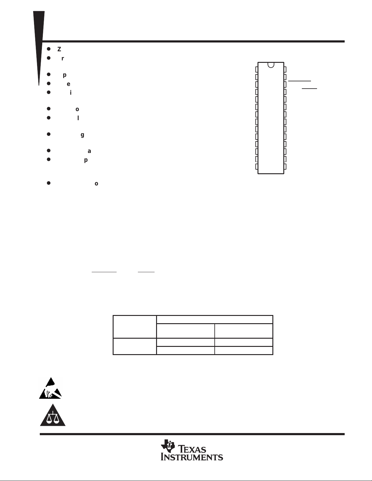
ANLG COMMON
AUTO ZERO
BUFF OUT
DW OR N PACKAGE
V
CC–
REF
INT OUT
C
ref–
C
ref+
IN–
IN+
V
CC+
D5
B1
B2
(TOP VIEW)
1
28
2
27
3
26
4
25
5
24
6
23
7
22
8
21
9
20
10
19
11
18
12
17
13
16
14
15
UNDER RANGE
OVER RANGE
STROBE
RUN/HOLD
DGTL GND
POLARITY
CLK
BUSY
D1
D2
D3
D4
B8
B4
Siliconix Si7135
D
CMOS Technology
description
The ICL7135C and TLC7135C converters are manufactured with Texas Instruments highly efficient CMOS
technology. These 4 1/2-digit, dual-slope-integrating, analog-to-digital converters (DACs) are designed to
provide interfaces to both a microprocessor and a visual display. The digit-drive outputs D1 through D4 and
multiplexed binary-coded-decimal outputs B1, B2, B4, and B8 provide an interface for LED or LCD
decoder/drivers as well as microprocessors.
The ICL7135C and TLC7135C offer 50-ppm (one part in 20,000) resolution with a maximum linearity error of
one count. The zero error is less than 10 µV and zero drift is less than 0.5 µV/°C. Source-impedance errors are
minimized by low input current (less than 10 pA). Rollover error is limited to ±1 count.
The BUSY, STROBE
, RUN/HOLD, OVER RANGE, and UNDER RANGE control signals support
microprocessor-based measurement systems. The control signals also can support remote data acquisition
systems with data transfer through universal asynchronous receiver transmitters (UARTs).
The ICL7135C and TLC7135C are characterized for operation from 0°C to 70°C.
AVAILABLE OPTIONS
PACKAGE
T
A
°
°
Caution. These devices have limited built-in protection. The leads should be shorted together or the device placed in conductive foam
during storage or handlilng to prevent electrostatic damage to the MOS gates.
Please be aware that an important notice concerning availability, standard warranty, and use in critical applications of
Texas Instruments semiconductor products and disclaimers thereto appears at the end of this data sheet.
PLASTIC DIP
(N)
ICL7135CN
TLC7135CN TLC7135CDW
SMALL OUTLINE
(DW)
PRODUCTION DATA information is current as of publication date.
Products conform to specifications per the terms of Texas Instruments
standard warranty. Production processing does not necessarily include
testing of all parameters.
POST OFFICE BOX 655303 • DALLAS, TEXAS 75265
Copyright 1999, Texas Instruments Incorporated
1
ICL7135C, TLC7135C
4 1/2-DIGIT PRECISION
ANALOG-TO-DIGITAL CONVERTERS
SLAS074B – DECEMBER 1986 – REVISED MA Y 1999
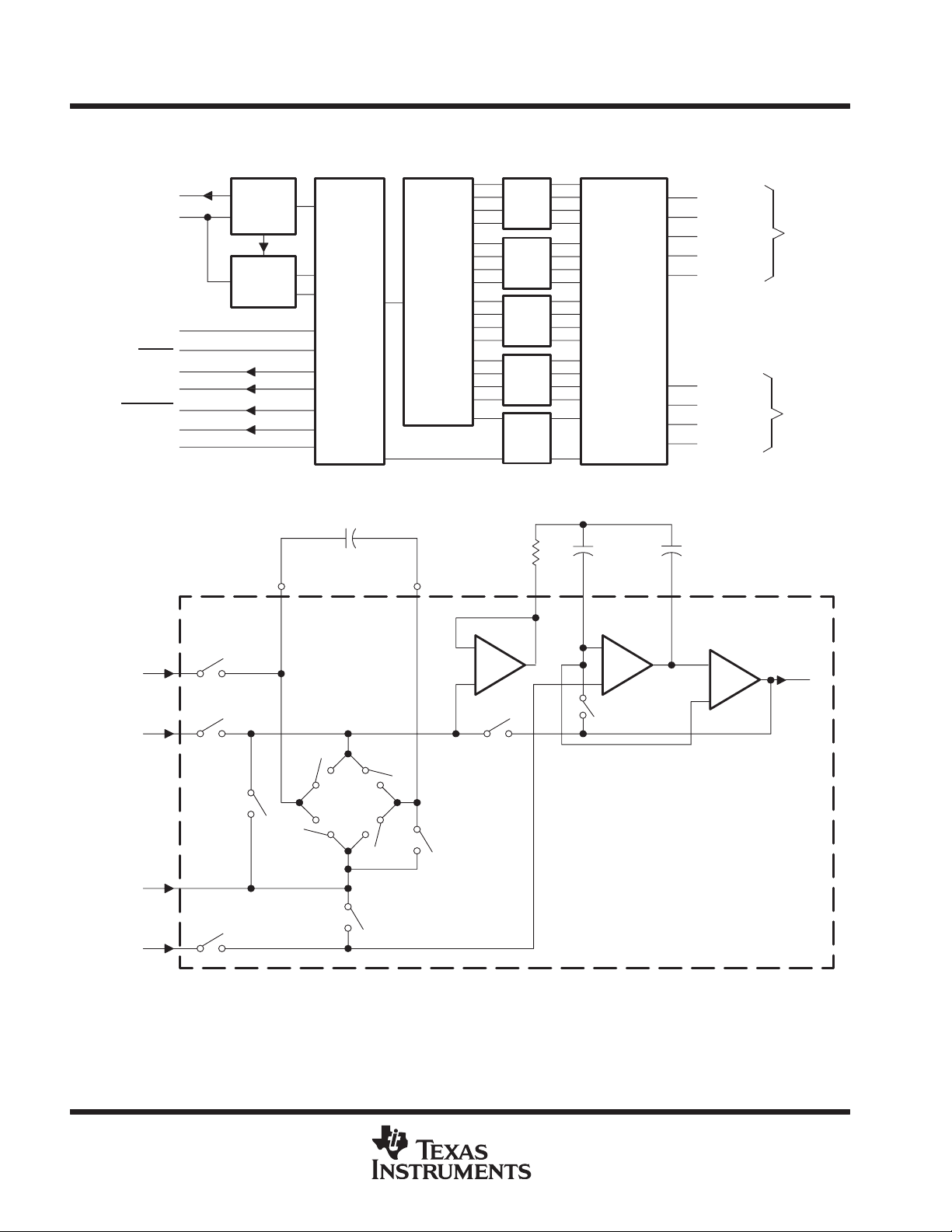
functional block diagram
DIGITAL SECTION
POLARITY
From Analog
Section
CLK
RUN/HOLD
OVER RANGE
UNDER RANGE
STROBE
BUSY
DGTL GND
2
REF
10
IN+
23
22
25
27
28
26
21
24
A/Z
INT
Polarity
Flip-Flop
Zero
Cross
Detect
8
C
ref+
DE(–)
Control
Logic
C
ref
Counters
ANALOG SECTION
C
DE(+)
ref–
7
Input
High
BUFF
OUT
Buffer
–
+
Z/I
Latch
Latch
Latch
Latch
Latch
6
20
D1 (LSD)
19
D2
18
D3
17
D4
12
D5 (MSD)
Multiplexer
13
B1 (LSB)
14
B2
15
B4
16
B8 (MSB)
R
INT
5
C
AZ
AUTO
ZERO
Integrator
–
+
A/Z
INT OUT
4
C
INT
Comparator
+
–
Digit
Drive
Output
Binary
Coded
Decimal
Output
To
Digital
Section
ANLG
COMMON
2
IN–
A/Z
A/Z
DE(+) DE(–)
3
9
INT
A/Z, DE(
POST OFFICE BOX 655303 • DALLAS, TEXAS 75265
±), Z/I
Input
Low
VOHHigh-level output voltage
V
IIInput leakage current, IN– and IN
V
0
pA
I
Positive supply current
f
0
mA
I
Negative supply current
f
0
mA
ICL7135C, TLC7135C
4 1/2-DIGIT PRECISION
ANALOG-TO-DIGITAL CONVERTERS
SLAS074B – DECEMBER 1986 – REVISED MA Y 1999
absolute maximum ratings over operating free-air temperature range (unless otherwise noted)
Supply voltage (V
Analog input voltage (IN– or IN+) V
Reference voltage range V
Clock input voltage range 0 V to V
Operating free-air temperature range, T
Storage temperature range, T
Lead temperature 1,6 mm (1/16 inch) from case for 10 seconds: N package 260°C. . . . . . . . . . . . . . . . . . . . .
†
Stresses beyond those listed under “absolute maximum ratings” may cause permanent damage to the device. These are stress ratings only, and
functional operation of the device at these or any other conditions beyond those indicated under “recommended operating conditions” is not
implied. Exposure to absolute-maximum-rated conditions for extended periods may affect device reliability.
with respect to V
CC+
. . . . . . . . . . . . . . . . . . . . . . . . . . . . . . . . . . . . . . . . . . . . . . . . . . . . . . . . . . .
. . . . . . . . . . . . . . . . . . . . . . . . . . . . . . . . . . . . . . . . . . . . . . . . . . . . . . . . . . . .
) 15 V. . . . . . . . . . . . . . . . . . . . . . . . . . . . . . . . . . . . . . . . . . . . . . . . . .
CC–
. . . . . . . . . . . . . . . . . . . . . . . . . . . . . . . . . . . . . . . . . . . . . . . . . . .
0°C to 70°C. . . . . . . . . . . . . . . . . . . . . . . . . . . . . . . . . . . . . . . . . . . . . .
–65°C to 150°C. . . . . . . . . . . . . . . . . . . . . . . . . . . . . . . . . . . . . . . . . . . . . . . . . . .
stg
A
CC–
CC–
to V
to V
CC+
CC+
CC+
recommended operating conditions
MIN NOM MAX UNIT
Supply voltage, V
Supply voltage, V
Reference voltage, V
High-level input voltage, CLK, RUN/HOLD, V
Low-level input voltage, CLK, RUN/HOLD, V
Differential input voltage, V
Maximum operating frequency, f
Operating free-air temperature range, T
NOTE 1: Clock frequency range extends down to 0 Hz.
CC+
CC–
ref
IH
IL
ID
(see Note 1) 1.2 2 MHz
clock
A
4 5 6 V
–3 –5 –8 V
1 V
2.8 V
0.8 V
V
+1 V
CC–
0 70 °C
–0.5 V
CC+
†
electrical characteristics, V
CC+
= 5 V, V
CC–
= 5 V, V
ref
otherwise noted)
PARAMETER TEST CONDITIONS MIN TYP MAX UNIT
p
V
OL
V
ON(PP)
α
VO
I
IH
I
IL
CC+
CC–
C
pd
NOTES: 2. This is the peak-to-peak value that is not exceeded 95% of the time.
Low-level output voltage IO = 1.6 mA 0.4 V
Peak-to-peak output noise voltage (see Note 2) VID = 0, Full scale = 2 V 15 µV
Zero-reading temperature coefficient of output voltage VID = 0, 0°C ≤ TA ≤ 70°C 0.5 2 µV/°C
High-level input current VI = 5 V, 0°C ≤TA ≤ 70°C 0.1 10 µA
Low-level input current VI = 0 V, 0°C ≤TA ≤ 70°C –0.02 –0.1 mA
p
pp
pp
Power dissipation capacitance See Note 3 40 pF
3. Factor-relating clock frequency to increase in supply current. At V
D1-D5,B1,B2,B4,B8 IO = –1 mA 2.4 5
Other outputs IO = –10 µA 4.9 5
+
ID
clock
clock
CC+
= 1 V, f
TA = 25°C 1 10
=
0°C ≤ TA ≤ 70°C 250
TA = 25°C 1 2
=
0°C ≤ TA ≤ 70°C 3
TA = 25°C –0.8 –2
=
0°C ≤ TA ≤ 70°C –3
= 5 V, I
= 120 kHz, TA = 25°C (unless
clock
CC+
= I
CC+(fclock
= 0) + Cpd × 5 V × f
p
clock
POST OFFICE BOX 655303 • DALLAS, TEXAS 75265
3
ICL7135C, TLC7135C
Display reading in ratiometric operation
g
4 1/2-DIGIT PRECISION
ANALOG-TO-DIGITAL CONVERTERS
SLAS074B – DECEMBER 1986 – REVISED MA Y 1999
operating characteristics, V
= 5 V, VCC– = 5 V, V
CC+
= 1 V, f
ref
= 120 kHz, TA = 25°C (unless
clock
otherwise noted)
PARAMETER TEST CONDITIONS MIN TYP MAX UNIT
α
Full-scale temperature coefficient (see Note 4) VID = 2 V, 0°C ≤ TA ≤ 70°C 5 ppm/°C
FS
E
Linearity error –2 V ≤VID ≤ 2 V 0.5 count
L
E
Differential linearity error (see Note 5) –2 V ≤VID ≤ 2 V 0.01 LSB
D
E
± Full-scale symmetry error (rollover error) (see Note 6) VID = ±2 V 0.5 1 count
FS
Display reading with 0-V input VID = 0, 0°C ≤TA ≤ 70°C –0.0000 ±0.0000 0.0000
p
NOTES: 4. This parameter is measured with an external reference having a temperature coefficient of less than 0.01 ppm/°C.
5. The magnitude of the difference between the worst case step of adjacent counts and the ideal step.
6. Rollover error is the difference between the absolute values of the conversion for 2 V and –2 V.
p
VID = V
0°C ≤ TA ≤ 70°C 0.9995 0.9999 1.0005
, TA = 25°C 0.9998 0.9999 1.0000
ref
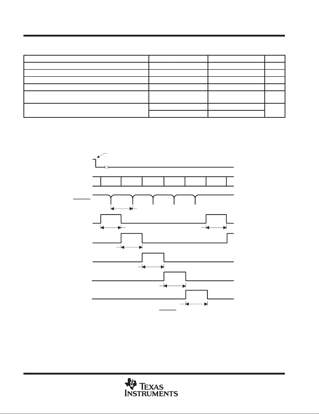
timing diagrams
End of Conversion
†
BUSY
B1–B8
D5D1D2D3D4D5
Digital
Reading
Digital
Reading
STROBE
†
†
200 Counts
D5
201 Counts
D4
200 Counts
D3
200 Counts
D2
200 Counts
D1
200 Counts
Delay between BUSY going low and the first STROBE
Figure 1
200 Counts
pulse is dependent upon the analog input.
4
POST OFFICE BOX 655303 • DALLAS, TEXAS 75265

timing diagrams (continued)
ICL7135C, TLC7135C
4 1/2-DIGIT PRECISION
ANALOG-TO-DIGITAL CONVERTERS
SLAS074B – DECEMBER 1986 – REVISED MA Y 1999
Integrator Output
Digital Scan
for OVER-RANGE
1000 Counts
AUTO ZERO
10,001 Counts
Figure 2
Signal Int
10,000
Counts
Full Measurement Cycle
40,002 Counts
De-Integrate
20,001 Counts Max
D5
D4
D3
D2
D1
BUSY
OVER RANGE
When Applicable
UNDER RANGE
When Applicable
Figure 3
POST OFFICE BOX 655303 • DALLAS, TEXAS 75265
5

ICL7135C, TLC7135C
4 1/2-DIGIT PRECISION
ANALOG-TO-DIGITAL CONVERTERS
SLAS074B – DECEMBER 1986 – REVISED MA Y 1999
timing diagrams (continued)
STROBE
AUTO ZERO
Digit Scan
for OVER RANGE
†
First D5 of AUTO ZERO and deintegrate is one count longer.
D5
†
D4
D3
D2
D1
Signal Integrate
Deintegrate
†
Figure 4
PRINCIPLES OF OPERATION
A measurement cycle for the ICL7135C and TLC7135C consists of the following four phases.
1. Auto-Zero Phase. The internal IN+ and IN– inputs are disconnected from the terminals and internally
connected to ANLG COMMON. The reference capacitor is charged to the reference voltage. The
system is configured in a closed loop and the auto-zero capacitor is charged to compensate for offset
voltages in the buffer amplifier , integrator, and comparator . The auto-zero accuracy is limited only by the
system noise, and the overall offset, as referred to the input, is less than 10 µV.
2. Signal Integrate Phase. The auto-zero loop is opened and the internal IN+ and IN– inputs are
connected to the external terminals. The differential voltage between these inputs is integrated for a
fixed period of time. When the input signal has no return with respect to the converter power supply , IN–
can be tied to ANLG COMMON to establish the correct common-mode voltage. Upon completion of this
phase, the polarity of the input signal is recorded.
3. Deintegrate Phase. The reference is used to perform the deintegrate task. The internal IN– is internally
connected to ANLG COMMON and IN+ is connected across the previously charged reference
capacitor. The recorded polarity of the input signal ensures that the capacitor is connected with the
correct polarity so that the integrator output polarity returns to zero. The time required for the output to
return to zero is proportional to the amplitude of the input signal. The return time is displayed as a digital
reading and is determined by the equation 10,000 × (V
occurs when V
is two times V
ID
ref
.
). The maximum or full-scale conversion
ID/Vref
4. Zero Integrator Phase. The internal IN– is connected to ANLG COMMON. The system is configured in a
closed loop to cause the integrator output to return to zero. Typically, this phase requires 100 to 200
clock pulses. However, after an over-range conversion, 6200 pulses are required.
6
POST OFFICE BOX 655303 • DALLAS, TEXAS 75265

ICL7135C, TLC7135C
4 1/2-DIGIT PRECISION
ANALOG-TO-DIGITAL CONVERTERS
SLAS074B – DECEMBER 1986 – REVISED MA Y 1999
PRINCIPLES OF OPERATION
description of analog circuits
input signal range
The common mode range of the input amplifier extends from 1 V above the negative supply to 1 V below the
positive supply . Within this range, the common-mode rejection ratio (CMRR) is typically 86 dB. Both differential
and common-mode voltages cause the integrator output to swing. Therefore, care must be exercised to ensure
that the integrator output does not become saturated.
analog common
Analog common (ANLG COMMON) is connected to the internal IN– during the auto-zero, deintegrate, and zero
integrator phases. When IN– is connected to a voltage that is different from analog common during the signal
integrate phase, the resulting common-mode voltage is rejected by the amplifier. However , in most applications,
IN– is set at a known fixed voltage (i.e., power supply common for instance). In this application, analog common
should be tied to the same point, thus removing the common-mode voltage from the converter. Removing the
common-mode voltage in this manner slightly increases conversion accuracy.
reference
The reference voltage is positive with respect to analog common. The accuracy of the conversion result is
dependent upon the quality of the reference. Therefore, to obtain a high accuracy conversion, a high quality
reference should be used.
description of digital circuits
RUN/HOLD input
When RUN/HOLD
pulses. When this input is taken low, the integrated circuit continues to perform the ongoing measurement cycle
and then hold the conversion reading for as long as the terminal is held low. When the terminal is held low after
completion of a measurement cycle, a short positive pulse (greater than 300 ns) initiates a new measurement
cycle. When this positive pulse occurs before the completion of a measurement cycle, it will not be recognized.
The first STROBE
completion of a measurement cycle. Thus, the positive pulse could be used to trigger the start of a new
measurement after the first STROBE
STROBE
input
Negative going pulses from this input transfer the BCD conversion data to external latches, UARTs, or
microprocessors. At the end of the measurement cycle, STROBE
The most significant digit (MSD) BCD bits are placed on the BCD terminals. After the first 101 counts, halfway
through the duration of output D1–D5 going high, the STROBE
placement of the STROBE
an external device on either a low-level or an edge. Such placement of the STROBE
the BCD bits for the second MSD are not yet competing for the BCD lines and latching of the correct bits is
ensured. The above process is repeated for the second MSD and the D4 output. Similarly, the process is
repeated through the least significant digit (LSD). Subsequently, inputs D5 through D1 and the BCD lines
continue scanning without the inclusion of STROBE
conversion results to be continuously displayed. Such subsequent scanning does not occur when an over-range
condition occurs.
is high or open, the device continuously performs measurement cycles every 40,002 clock
pulse, which occurs 101 counts after the end of a measurement cycle, is an indication of the
pulse.
goes high and remains high for 201 counts.
terminal goes low for 1/2 clock pulse width. The
pulse at the midpoint of the D5 high pulse allows the information to be latched into
pulse also ensures that
pulses. This subsequent continuous scanning causes the
POST OFFICE BOX 655303 • DALLAS, TEXAS 75265
7

ICL7135C, TLC7135C
4 1/2-DIGIT PRECISION
ANALOG-TO-DIGITAL CONVERTERS
SLAS074B – DECEMBER 1986 – REVISED MA Y 1999
PRINCIPLES OF OPERATION
BUSY output
The BUSY output goes high at the beginning of the signal integrate phase. BUSY remains high until the first
clock pulse after zero crossing or at the end of the measurement cycle when an over-range condition occurs.
It is possible to use the BUSY terminal to serially transmit the conversion result. Serial transmission can be
accomplished by ANDing the BUSY and CLOCK signals and transmitting the ANDed output. The transmitted
output consists of 10,001 clock pulses, which occur during the signal integrate phase, and the number of clock
pulses that occur during the deintegrate phase. The conversion result can be obtained by subtracting 10,001
from the total number of clock pulses.
OVER-RANGE output
When an over-range condition occurs, this terminal goes high after the BUSY signal goes low at the end of the
measurement cycle. As previously noted, the BUSY signal remains high until the end of the measurement cycle
when an over-range condition occurs. The OVER RANGE output goes high at the end of BUSY and goes low
at the beginning of the deintegrate phase in the next measurement cycle.
UNDER-RANGE output
At the end of the BUSY signal, this terminal goes high when the conversion result is less than or equal to 9%
(count of 1800) of the full-scale range. The UNDER-RANGE output is brought low at the beginning of the signal
integrate phase of the next measurement cycle.
POLARITY output
The POLARITY output is high for a positive input signal and updates at the beginning of each deintegrate phase.
The polarity output is valid for all inputs including ±0 and OVER RANGE signals.
digit-drive (D1, D2, D4 and D5) outputs
Each digit-drive output (D1 through D5) sequentially goes high for 200 clock pulses. This sequential process
is continuous unless an over-range occurs. When an over-range occurs, all of the digit-drive outputs are blanked
from the end of the strobe sequence until the beginning of the deintegrate phase (when the sequential digit-drive
activation begins again). The blanking activity during an over-range condition can cause the display to flash and
indicate the over-range condition.
BCD outputs
The BCD bits (B1, B2, B4 and B8) for a given digit are sequentially activated on these outputs. Simultaneously ,
the appropriate digit-drive line for the given digit is activated.
system aspects
integrating resistor
The value of the integrating resistor (R
of the integrating amplifier. The integrating amplifier can supply 20 µA of current with negligible nonlinearity . The
equation for determining the value of this resistor is:
R
INT
Full Scale Voltage
+
I
INT
) is determined by the full-scale input voltage and the output current
INT
Integrating amplifier current, I
current is 20 µA.
8
, from 5 to 40 µA yields good results. However, the nominal and recommended
INT
POST OFFICE BOX 655303 • DALLAS, TEXAS 75265

ICL7135C, TLC7135C
4 1/2-DIGIT PRECISION
ANALOG-TO-DIGITAL CONVERTERS
SLAS074B – DECEMBER 1986 – REVISED MA Y 1999
PRINCIPLES OF OPERATION
integrating capacitor
The product of the integrating resistor and capacitor should be selected to give the maximum voltage swing
without causing the integrating amplifier output to saturate and get too close to the power supply voltages. When
the amplifier output is within 0.3 V of either supply , saturation occurs. With ±5-V supplies and ANLG COMMON
connected to ground, the designer should design for a ±3.5-V to ±4-V integrating amplifier swing. A nominal
capacitor value is 0.47 µF. The equation for determining the value of the integrating capacitor (C
C
INT
Where:
I
INT
Capacitors with large tolerances and high dielectric absorption can induce conversion inaccuracies. A capacitor
that is too small could cause the integrating amplifier to saturate. High dielectric absorption causes the effective
capacitor value to be different during the signal integrate and deintegrate phases. Polypropylene capacitors
have very low dielectric absorption. Polystyrene and polycarbonate capacitors have higher dielectric
absorption, but also work well.
10,000 Clock Period I
+
Integrator Output Voltage Swing
is nominally 20 µA.
INT
INT
) is:
auto-zero and reference capacitor
Large capacitors tend to reduce noise in the system. Dielectric absorption is unimportant except during power
up or overload recovery. Typical values are 1 µF.
reference voltage
For high-accuracy absolute measurements, a high quality reference should be used.
rollover resistor and diode
The ICL7135C and TLC7135C have a small rollover error; however, it can be corrected. The correction is to
connect the cathode of any silicon diode to INT OUT and the anode to a resistor. The other end of the resistor
is connected to ANLG COMMON or ground. For the recommended operating conditions, the resistor value is
100 kΩ. This value may be changed to correct any rollover error that has not been corrected. In many noncritical
applications the resistor and diode are not needed.
maximum clock frequency
For most dual-slope A/D converters, the maximum conversion rate is limited by the frequency response of the
comparator. In this circuit, the comparator follows the integrator ramp with a 3-µs delay. Therefore, with a
160-kHz clock frequency (6-µs period), half of the first reference integrate clock period is lost in delay . Hence,
the meter reading changes from 0 to 1 with a 50-µV input, 1 to 2 with a 150-µV input, 2 to 3 with a 250-µV input,
etc. This transition at midpoint is desirable; however, when the clock frequency is increased appreciably above
160 kHz, the instrument flashes 1 on noise peaks even when the input is shorted. The above transition points
assume a 2-V input range is equivalent to 20,000 clock cycles.
When the input signal is always of one polarity , comparator delay need not be a limitation. Clock rates of 1 MHz
are possible since nonlinearity and noise do not increase substantially with frequency. For a fixed clock
frequency, the extra count or counts caused by comparator delay are a constant and can be subtracted out
digitally.
For signals with both polarities, the clock frequency can be extended above 160 kHz without error by using a
low value resistor in series with the integrating capacitor. This resistor causes the integrator to jump slightly
towards the zero-crossing level at the beginning of the deintegrate phase, and thus compensates for the
comparator delay. This series resistor should be 10 Ω to 50 Ω. This approach allows clock frequencies up to
480 kHz.
POST OFFICE BOX 655303 • DALLAS, TEXAS 75265
9

ICL7135C, TLC7135C
4 1/2-DIGIT PRECISION
ANALOG-TO-DIGITAL CONVERTERS
SLAS074B – DECEMBER 1986 – REVISED MA Y 1999
PRINCIPLES OF OPERATION
minimum clock frequency
The minimum clock frequency limitations result from capacitor leakage from the auto-zero and reference
capacitors. Measurement cycles as high as 10 µs are not influenced by leakage error.
rejection of 50-Hz or 60-Hz pickup
To maximize the rejection of 50-Hz or 60-Hz pickup, the clock frequency should be chosen so that an integral
multiple of 50-Hz or 60-Hz periods occur during the signal integrate phase. T o achieve rejection of these signals,
some clock frequencies that can be used are:
50 Hz: 250, 166.66, 125, 100 kHz, etc.
60 Hz: 300, 200, 150, 120, 100, 40, 33.33 kHz, etc.
zero-crossing flip-flop
This flip-flop interrogates the comparator’s zero-crossing status. The interrogation is performed after the
previous clock cycle and the positive half of the ongoing clock cycle has occurred, so any comparator transients
that result from the clock pulses do not affect the detection of a zero-crossing. This procedure delays the
zero-crossing detection by one clock cycle. To eliminate the inaccuracy, which is caused by this delay, the
counter is disabled for one clock cycle at the beginning of the deintegrate phase. Therefore, when the
zero-crossing is detected one clock cycle later than the zero-crossing actually occurs, the correct number of
counts is displayed.
noise
The peak-to-peak noise around zero is approximately 15 µV (peak-to-peak value not exceeded 95% of the
time). Near full scale, this value increases to approximately 30 µV . Much of the noise originates in the auto-zero
loop, and is proportional to the ratio of the input signal to the reference.
analog and digital grounds
For high-accuracy applications, ground loops must be avoided. Return currents from digital circuits must not
be sent to the analog ground line.
power supplies
The ICL7135C and TLC7135C are designed to work with ± 5-V power supplies. However, 5-V operation is
possible when the input signal does not vary more than ±1.5 V from midsupply.
10
POST OFFICE BOX 655303 • DALLAS, TEXAS 75265

IMPORTANT NOTICE
T exas Instruments and its subsidiaries (TI) reserve the right to make changes to their products or to discontinue
any product or service without notice, and advise customers to obtain the latest version of relevant information
to verify, before placing orders, that information being relied on is current and complete. All products are sold
subject to the terms and conditions of sale supplied at the time of order acknowledgement, including those
pertaining to warranty, patent infringement, and limitation of liability.
TI warrants performance of its semiconductor products to the specifications applicable at the time of sale in
accordance with TI’s standard warranty. Testing and other quality control techniques are utilized to the extent
TI deems necessary to support this warranty . Specific testing of all parameters of each device is not necessarily
performed, except those mandated by government requirements.
CERT AIN APPLICATIONS USING SEMICONDUCTOR PRODUCTS MAY INVOL VE POTENTIAL RISKS OF
DEATH, PERSONAL INJURY, OR SEVERE PROPERTY OR ENVIRONMENTAL DAMAGE (“CRITICAL
APPLICATIONS”). TI SEMICONDUCTOR PRODUCTS ARE NOT DESIGNED, AUTHORIZED, OR
WARRANTED TO BE SUITABLE FOR USE IN LIFE-SUPPORT DEVICES OR SYSTEMS OR OTHER
CRITICAL APPLICA TIONS. INCLUSION OF TI PRODUCTS IN SUCH APPLICATIONS IS UNDERST OOD TO
BE FULLY AT THE CUSTOMER’S RISK.
In order to minimize risks associated with the customer’s applications, adequate design and operating
safeguards must be provided by the customer to minimize inherent or procedural hazards.
TI assumes no liability for applications assistance or customer product design. TI does not warrant or represent
that any license, either express or implied, is granted under any patent right, copyright, mask work right, or other
intellectual property right of TI covering or relating to any combination, machine, or process in which such
semiconductor products or services might be or are used. TI’s publication of information regarding any third
party’s products or services does not constitute TI’s approval, warranty or endorsement thereof.
Copyright 1999, Texas Instruments Incorporated
 Loading...