

Page 1
HPC3130
PCI HOT PLUG CONTROLLER
SCPS029B – DECEMBER1998
1
POST OFFICE BOX 655303 • DALLAS, TEXAS 75265
D
Compliant with PCI Hot-Plug Specification,
Revision 1.0
D
Supports up to Four Independently
Controlled Hot-Plug Slots
D
Provides Register Accessing Through Both
Generic Parallel Bus and Two-Wire Serial
Interface
D
Provides Interrupt and Event Status/Enable
State Compliant with ACPI Specification 1.0
D
Provides an Automatic Bus Connection
Sequencing Feature
D
Supports 66-MHz PCI Clock Frequency
D
Features Two Attention Indicators with
Variable LED Blinking Rates per Slot
D
Provides an Easy Scheme to Cascade the
HPC3130 for Compact PCI Applications
D
Provides Card Detection Mechanism
Independent of PCI Present Signals for
Advanced Card Protection
D
Provides Path to Guarantee Idle State
During PCI Bus Connections
D
Fabricated in Advanced Low-Power CMOS
Process
D
Features a CBT Switch† Control Feature for
REQ64
Implementation
D
Package Options:
– 120-pin QFP Package
– 128-pin LQFP Package
– 144-pin LQFP Package
Table of Contents
Description 2. . . . . . . . . . . . . . . . . . . . . . . . . . . . . . . . . . . . . . . . . . . . . . . . 66 MHz PCI Support 24. . . . . . . . . . . . . . . . . . . . . . . . . . . . . . . . . . . . . . .
Functional Block Diagram 2. . . . . . . . . . . . . . . . . . . . . . . . . . . . . . . . . . . Configuration and Control Registers 25. . . . . . . . . . . . . . . . . . . . . . . . .
Pin Assignments (120-Pin) 3. . . . . . . . . . . . . . . . . . . . . . . . . . . . . . . . . . Absolute Maximum Ratings 32. . . . . . . . . . . . . . . . . . . . . . . . . . . . . . . . .
Pin Assignments (128-Pin) 4. . . . . . . . . . . . . . . . . . . . . . . . . . . . . . . . . . Recommended Operating Conditions 33. . . . . . . . . . . . . . . . . . . . . . . .
Pin Assignments (144-Pin) 5. . . . . . . . . . . . . . . . . . . . . . . . . . . . . . . . . . Serial Bus Interface 34. . . . . . . . . . . . . . . . . . . . . . . . . . . . . . . . . . . . . . .
Signal Name/Pin Number Sort Table (120-Pin) 6. . . . . . . . . . . . . . . . . Electrical Characteristics 34. . . . . . . . . . . . . . . . . . . . . . . . . . . . . . . . . . .
Signal Name/Pin Number Sort Table (128-Pin) 8. . . . . . . . . . . . . . . . . PCI Clock/Reset Timing Requirements 35. . . . . . . . . . . . . . . . . . . . . . .
Signal Name/Pin Number Sort Table (144-Pin) 10. . . . . . . . . . . . . . . . PCI Timing Requirements 36. . . . . . . . . . . . . . . . . . . . . . . . . . . . . . . . . .
Terminal Functions 12. . . . . . . . . . . . . . . . . . . . . . . . . . . . . . . . . . . . . . . . Mechanical Data (120-Pin) 37. . . . . . . . . . . . . . . . . . . . . . . . . . . . . . . . .
HPC3130 Applications 15. . . . . . . . . . . . . . . . . . . . . . . . . . . . . . . . . . . . . Mechanical Data (128-Pin) 38. . . . . . . . . . . . . . . . . . . . . . . . . . . . . . . . .
SLOTREQ64 23. . . . . . . . . . . . . . . . . . . . . . . . . . . . . . . . . . . . . . . . . . . . . Mechanical Data (144-Pin) 39. . . . . . . . . . . . . . . . . . . . . . . . . . . . . . . . .
Copyright 1998, Texas Instruments Incorporated
Please be aware that an important notice concerning availability, standard warranty, and use in critical applications of
Texas Instruments semiconductor products and disclaimers thereto appears at the end of this data sheet.
†
Contact Texas Instrument’s Bus Interface product group for information related to CBT switches.
PRODUCTION DATA information is current as of publication date.
Products conform to specifications per the terms of Texas Instruments
standard warranty. Production processing does not necessarily include
testing of all parameters.
Page 2
HPC3130
PCI HOT PLUG CONTROLLER
SCPS029B – DECEMBER1998
2
POST OFFICE BOX 655303 • DALLAS, TEXAS 75265
description
The Texas Instruments HPC3130 is a peripheral component interconnect (PCI) hot-plug controller, compliant
with
PCI Hot-Plug Specification, Revision 1.0
. This device supports hot insertion/removal of up to four hot-plug
slots on a PCI bus, provides a 64-bit data path in any of the four hot-plug slots, and supports 66-MHz systems
for two slots.
The primary function of the HPC3130 is to allow noninterfering hot-plug slot connection/disconnection with the
other PCI devices on the bus. The HPC3130 provides automatic bus connection sequencing and supports a
protocol for connection during bus idle conditions. It also supports an interrupt pin to report hot-plug slot events.
The interrupt event status and enable state are compliant with the
Advanced Configuration and Power Interface
(ACPI) Specification
.
Internal registers may be accessed through either a two-signal serial interface or a generic parallel bus. The
serial interface slave decoding circuit supports up to eight different controllers or other serial bus devices with
the same system base. Decoding through the parallel interface supports multiple controllers with external
chip-select logic. Two double-words of configuration and control registers are provided per slot. As a result, the
HPC3130 decodes an address range of 32 bytes.
An advanced complementary metal-oxide semiconductor (CMOS) process provides low system power
consumption while operating at PCI clock rates up to 66 MHz.
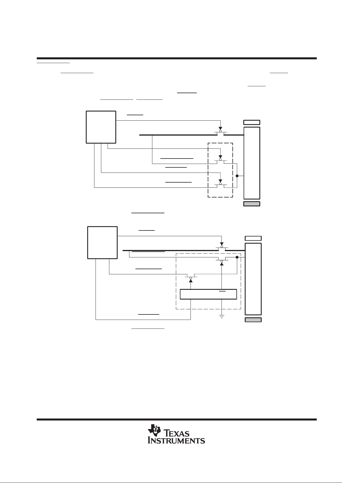
functional block diagram
A simplified block diagram of the HPC3130 is provided below. The block diagram illustrates the HPC3130
functionality on a per slot basis. The SMODE chip input, not shown, is used for terminal multiplexing of the serial
and parallel bus slave interfaces.
CS
Parallel
Bus
Slave
Interface
Serial Bus
Slave I/F
Switch
Timing
Control
and
Status
Registers
Slot
Power I/F
Card
Detection
CBT-Switch
Control
and
Slot Reset
Attention
Indicators
RD
WR
DATA 7–0
A 4–0
SDA
SCL
ADD 6–0
IDLEREQ
IDLEGNT
FRAME
IRDY
SREQ
SGNT
PCLK
PWRON/OFF
PWRFAULT
PWRGOOD
PRSNT2
PRSNT1
REQ64ON
REQ64ON
CLKON
SLOTRST
SLOTREQ64
ATTN0
ATTN1
SYSM66EN
INTR
PRST
BUSON
M66EN
DETECT
SYSTEM INTERFACE SLOT INTERFACE
Page 3
HPC3130
PCI HOT PLUG CONTROLLER
SCPS029B – DECEMBER1998
3
POST OFFICE BOX 655303 • DALLAS, TEXAS 75265
pin assignments (120-pin package)
PBM QUAD FLAT PACKAGE
TOP VIEW
PRST
PWRON/OFF[3]
1
2
3
4
5
6
7
8
9
10
11
12
13
14
15
16
17
18
19
20
21
22
23
24
25
26
27
28
29
93
94
95
96
97
98
99
100
101
102
103
104
105
106
107
108
109
110
111
112
113
114
115
116
117
118
119
120
90
89
88
87
86
85
84
83
82
81
80
79
78
77
76
75
74
73
72
71
70
69
68
67
66
65
64
63
62
59
58
57
56
55
54
53
52
51
50
49
48
47
46
45
44
43
42
41
40
39
38
37
36
35
34
33
32
31
91
92
60
30
61
RSVD
RSVD
DETECT1[1]
DETECT0[1]
M66EN[1]
ATTN1[1]
ATTN0[1]
CLKON[1]
BUSON[1]
REQ64ON[1]
GND
REQ64ON[1]
SLOTRST[1]
PRSNT2[1]
PWRGOOD[1]
DETECT1[0]
DETECT0[0]
GND
M66EN[0]
ATTN1[0]
ATTN0[0]
CLKON[0]
BUSON[0]
RSVD
RSVD
PWRFAULT[1]
ATTN0[3]
M66EN[3]
DETECT0[3]
SLOTREQ64[3]
SLOTREQ64[2]
SLOTREQ64[1]
SLOTREQ64[0]
GND
SREQ
SGNT
SMODE
PCLK
GND
IDLEREQ
IDLEGNT
FRAME
IRDY
INTR
INTR
SYSM66EN
GND
RD/SDA
WR/SCL
CLKON[3]
BUSON[3]
REQ64ON[3]
GND
REQ64ON[3]
SLOTRST[3]
PRSNT2[3]
PRSNT1[3]
GND
PWRGOOD[3]
DETECT1[2]
DETECT0[2]
M66EN[2]
ATTN1[2]
ATTN0[2]
CLKON[2]
GND
BUSON[2]
REQ640N[2]
REQ64ON[2]
SLOTRST[2]
PRSNT2[2]
PRSNT1[2]
PWRGOOD[2]
PWRFAULT[2]
PWRON/OFF[2]
RSVD
RSVD
RSVD
CS
DATA7
DATA6
DATA4
DATA3
GND
DATA2
DATA1/ADD6
DATA0/ADD5
A4/ADD4
A2/ADD2
A1/ADD1
GND
PWRON/OFF[0]
PWRFAULT[0]
PWRGOOD[0]
PRSNT1[0]
PRSNT2[0]
SLOTRST[0]
REQ64ON[0]
V
CC
ATTN1[3]
V
CC5V
CC
V
CC
V
A3/ADD3
CC
V
V
CC
V
CCP
V
CC5V
DETECT1[3]
V
CC5V
PRSNT1[1]
PWRON/OFF[1]
5V
PWRFAULT[3]
CC
V
DATA5
CC
V
5V
REQ64ON[0]
A0/ADD0
Page 4
HPC3130
PCI HOT PLUG CONTROLLER
SCPS029B – DECEMBER1998
4
POST OFFICE BOX 655303 • DALLAS, TEXAS 75265
pin assignments (128-pin package)
PBK LOW-PROFILE QUAD FLAT PACKAGE
TOP VIEW
GND
A0/ADD0
1
2
3
4
5
6
7
8
9
10
11
12
13
14
15
16
17
18
19
20
21
22
23
24
25
26
27
28
29
101
102
96
95
94
93
92
91
90
89
88
87
86
85
84
83
82
81
80
79
78
77
76
75
74
73
72
71
70
69
68
61
60
59
58
57
56
55
54
53
52
51
50
49
48
47
46
45
44
43
42
41
40
39
38
37
36
35
34
33
99
100
62
30
67
NC
RSVD
RSVD
DETECT1[1]
DETECT0[1]
ATTN1[1]
ATTN0[1]
CLKON[1]
BUSON[1]
REQ64ON[1]
GND
REQ64ON[1]
SLOTRST[1]
PRSNT2[1]
PRSNT1[1]
PWRFAULT[1
PWRON/OFF[1]
DETECT1[0]
DETECT0[0]
GND
M66EN[0]
ATTN1[0]
ATTN0[0]
CLKON[0]
BUSON[0]
RSVD
NC
ATTN1[3]
M66EN[3]
DETECT0[3]
DETECT1[3]
SLOTREQ64[3]
SLOTREQ64[2]
SLOTREQ64[1]
SLOTREQ64[0]
GND
SGNT
PRST
PCLK
GND
IDLEREQ
IDLEGNT
FRAME
IRDY
INTR
INTR
GND
SMODE
RD/SDA
NC
CLKON[3]
BUSON[3]
REQ64ON[3]
GND
REQ64ON[3]
SLOTRST[3]
PRSNT2[3]
PRSNT1[3]
GND
PWRGOOD[3]
PWRON/OFF[3]
DETECT1[2]
DETECT0[2]
M66EN[2]
ATTN1[2]
ATTN0[2]
CLKON[2]
GND
BUSON[2]
REQ64ON[2]
REQ64ON[2]
PRSNT2[2]
PRSNT1[2]
PWRGOOD[2]
PWRFAULT[2]
NC
RSVD
RSVD
RSVD
CS
DATA7
DATA6
DATA5
DATA4
DATA3
GND
DATA2
DATA1/ADD6
DATA0/ADD5
A4/ADD4
A3/ADD3
A2/ADD2
PWRON/OFF[0]
PWRFAULT[0]
PWRGOOD[0]
PRSNT1[0]
NC
PRSNT2[0]
SLOTRS[0]
REQ64ON[0]
V
CC
V
CC
V
CC5V
CC
V
CC
V
CC
V
32
WR/SCL
NC
31
63
64
97
98
PWRON/OFF[2]
NC
66
65
RSVD
NC
103
104
105
106
107
108
109
110
111
112
113
114
115
116
117
118
119
120
121
122
123
124
125
126
127
128
ATTN0[3]
M66EN[1]
SREQ
V
CC5V
PWRGOOD[1]
]
V
CCP
SYSM66EN
V
CC5V
PWRFAULT[3]
5V
SLOTRST[2]
CC
V
CC
V
5V
A1/ADD1
REQ64ON[0]
Page 5

HPC3130
PCI HOT PLUG CONTROLLER
SCPS029B – DECEMBER1998
5
POST OFFICE BOX 655303 • DALLAS, TEXAS 75265
pin assignments (144-pin package)
PGE LOW-PROFILE QUAD FLAT PACKAGE
TOP VIEW
PRSNT1[2]
SLOTRST[1]
CC
V
1234567891011121314151617181920212223242526272829303132333435
36
37
38
39
40
41
42
43
44
45
46
47
48
49
50
51
52
53
54
55
56
57
58
59
60
61
62
63
64
65
66
67
68
69
70
71
72
73
74
75
76
77
78
79
80
81
82
83
84
85
86
87
88
89
90
91
92
93
94
95
96
97
98
99
100
101
102
103
104
105
106
107
108
109
110
111
112
113
114
115
116
117
118
119
120
121
122
123
124
125
126
127
128
129
130
131
132
133
134
135
136
137
138
139
140
141
142
143
144
ATTN0[3]
NC
NC
M66EN[3]
NC
GND
PCLK
DETECT0[3]
IDLEGNT
FRAME
IRDY
IDLEREQ
SYSM66EN
GND
SMODE
NC
NC
NC
RSVD
NC
NC
RSVD
NC
DATA7
DATA6
DATA5
DATA3
GND
DATA2
DATA0/ADD5
A4/ADD4
A1/ADD1
NC
NC
A0/ADD0
GND
NC
RSVD
NC
ATTN0[0]
ATTN1[0]
M66EN[0]
GND
BUSON[0]
PRSNT1[1]
REQ64ON[1]
GND
REQ64ON[1]
ATTN0[1]
ATTN1[1]
M66EN[1]
NC
NC
RSVD
NC
NC
NC
NC
REQ64ON[2]
ATTN0[2]
ATTN1[2]
M66EN[2]
GND
GND
NC
REQ64ON[3]
NC
NC
PWRGOOD
[3]
PWRON/OFF
[2]
SREQ
CC5V
V
V
CC
CS
PWRFAULT[3]
V
CC
CC
V
CC5V
V
PWRFAULT[2]
NC
PWRGOOD
[2]
PRSNT2[2]
REQ64ON
[2]
BUSON[2]
SLOTRST[2]
CLKON[2]
DETECT0
[2]
V
CC5V
PWRON/OFF
[3]
DETECT1
[2]
GND
PRSNT1
[3]
PRSNT2[3]
SLOTRST[3]
REQ64ON
[3]
BUSON[3]
CLKON[3]
RSVD
DATA4
DATA1/ADD6
V
CC5V
A3/ADD3
A2/ADD2
PWRON/OFF
[0]
V
CC
PWRFAULT
[0]
PWRGOOD
[0]
PRSNT1
[0]
PRSNT2[0]
SLOTRST[0]
REQ64ON[0]
NC
REQ64ON[0]
RSVD
CLKON[0]
DETECT0[0]
DETECT1[0]
PWRON/OFF[1]
PWRFAULT[1]
PWRGOOD[1]
PRSNT2[1]
BUSON[1]
CLKON[1]
DETECT0[1]
DETECT1[1]
RSVD
ATTN1[3]
GND
DETECT1[3]
SLOTREQ64[3]
SLOTREQ64[2]
SLOTREQ64[1]
SLOTREQ64[0]
SGNT
PRST
CCP
V
INTR
INTR
CC5V
V
RD/SDA
WR/SCL
Page 6
HPC3130
PCI HOT PLUG CONTROLLER
SCPS029B – DECEMBER1998
6
POST OFFICE BOX 655303 • DALLAS, TEXAS 75265
signal names by terminal name
Table 1. Signals Sorted Alphabetically by Terminal Name (120-Pin Package)
TERMINAL NAME NO TERMINAL NAME NO TERMINAL NAME NO
A0/ADD0 50 GND 17 RD/SDA 29
A1/ADD1 49 GND 26 REQ64ON[0] 59
A2/ADD2 48 GND 41 REQ64ON[1] 78
A3/ADD3 47 GND 51 REQ64ON[2] 98
A4/ADD4 45 GND 68 REQ64ON[3] 116
ATTN0[0] 65 GND 79 REQ64ON[0] 60
ATTN0[1] 83 GND 101 REQ64ON[1] 80
ATTN0[2] 103 GND 112 REQ64ON[2] 99
ATTN0[3] 1 GND 117 REQ64ON[3] 118
ATTN1[0] 66 IDLEGNT 19 RSVD 31
ATTN1[1] 84 IDLEREQ 18 RSVD 32
ATTN1[2] 104 INTR 24 RSVD 33
ATTN1[3] 2 INTR 23 RSVD 61
BUSON[0] 63 IRDY 21 RSVD 62
BUSON[1] 81 M66EN[0] 67 RSVD 89
BUSON[2] 100 M66EN[1] 86 RSVD 90
BUSON[3] 119 M66EN[2] 105 SGNT 13
CLKON[0] 64 M66EN[3] 3 SLOTREQ64[0] 10
CLKON[1] 82 PCLK 16 SLOTREQ64[1] 9
CLKON[2] 102 PRSNT1[0] 55 SLOTREQ64[2] 8
CLKON[3] 120 PRSNT1[1] 75 SLOTREQ64[3] 7
CS 34 PRSNT1[2] 94 SLOTRST[0] 58
DATA0/ADD5 44 PRSNT1[3] 113 SLOTRST[1] 77
DATA1/ADD6 43 PRSNT2[0] 57 SLOTRST[2] 97
DATA2 42 PRSNT2[1] 76 SLOTRST[3] 115
DATA3 40 PRSNT2[2] 96 SMODE 27
DATA4 39 PRSNT2[3] 114 SREQ 12
DATA5 38 PRST 14 SYSM66EN 25
DATA6 37 PWRFAULT[0] 53 V
CC
6
DATA7 35 PWRFAULT[1] 72 V
CC
36
DETECT0[0] 69 PWRFAUL T[2] 92 V
CC
56
DETECT0[1] 87 PWRFAUL T[3] 110 V
CC
85
DETECT0[2] 106 PWRGOOD[0] 54 V
CC
95
DETECT0[3] 4 PWRGOOD[1] 73 V
CC5V
15
DETECT1[0] 70 PWRGOOD[2] 93 V
CC5V
28
DETECT1[1] 88 PWRGOOD[3] 111 V
CC5V
46
DETECT1[2] 108 PWRON/OFF[0] 52 V
CC5V
74
DETECT1[3] 5 PWRON/OFF[1] 71 V
CC5V
107
FRAME 20 PWRON/OFF[2] 91 V
CCP
22
GND 11 PWRON/OFF[3] 109 WR/SCL 30
Page 7
HPC3130
PCI HOT PLUG CONTROLLER
SCPS029B – DECEMBER1998
7
POST OFFICE BOX 655303 • DALLAS, TEXAS 75265
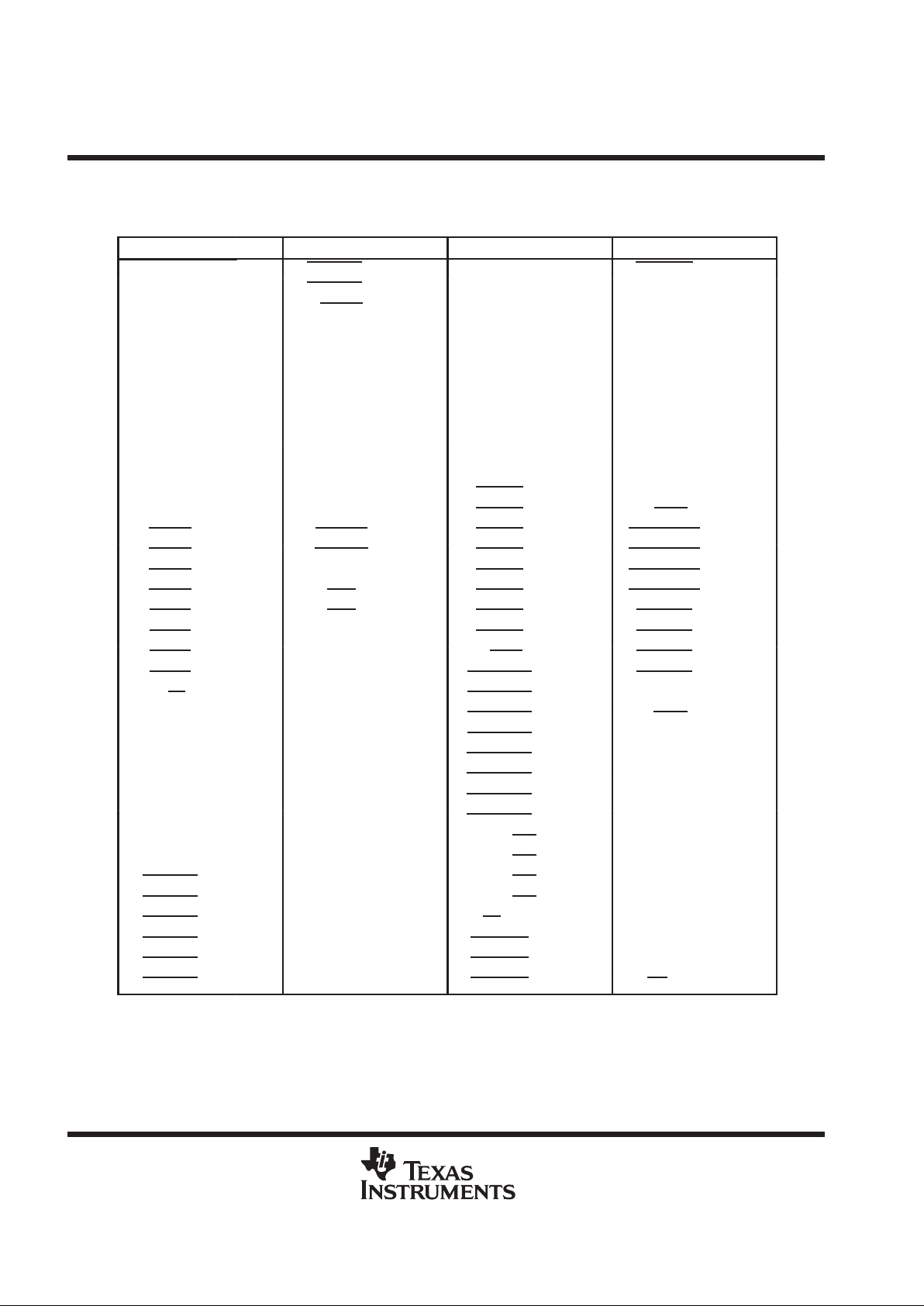
signal names by pin number
Table 2. Signals Sorted Numerically by Pin Number (120-Pin Package)
NO TERMINAL NAME NO TERMINAL NAME NO TERMINAL NAME
1 ATTN0[3] 41 GND 81 BUSON[1]
2 ATTN1[3] 42 DATA2 82 CLKON[1]
3 M66EN[3] 43 DATA1/ADD6 83 ATTN0[1]
4 DETECT0[3] 44 DATA0/ADD5 84 ATTN1[1]
5 DETECT1[3] 45 A4/ADD4 85 V
CC
6 V
CC
46 V
CC5V
86 M66EN[1]
7 SLOTREQ64[3] 47 A3/ADD3 87 DETECT0[1]
8 SLOTREQ64[2] 48 A2/ADD2 88 DETECT1[1]
9 SLOTREQ64[1] 49 A1/ADD1 89 RSVD
10 SLOTREQ64[0] 50 A0/ADD0 90 RSVD
11 GND 51 GND 91 PWRON/OFF[2]
12 SREQ 52 PWRON/OFF[0] 92 PWRFAULT[2]
13 SGNT 53 PWRFAUL T[0] 93 PWRGOOD[2]
14 PRST 54 PWRGOOD[0] 94 PRSNT1[2]
15 V
CC5V
55 PRSNT1[0] 95 V
CC
16 PCLK 56 V
CC
96 PRSNT2[2]
17 GND 57 PRSNT2[0] 97 SLOTRST[2]
18 IDLEREQ 58 SLOTRST[0] 98 REQ64ON[2]
19 IDLEGNT 59 REQ64ON[0] 99 REQ64ON[2]
20 FRAME 60 REQ64ON[0] 100 BUSON[2]
21 IRDY 61 RSVD 101 GND
22 V
CCP
62 RSVD 102 CLKON[2]
23 INTR 63 BUSON[0] 103 ATTN0[2]
24 INTR 64 CLKON[0] 104 ATTN1[2]
25 SYSM66EN 65 ATTN0[0] 105 M66EN[2]
26 GND 66 ATTN1[0] 106 DETECT0[2]
27 SMODE 67 M66EN[0] 107 V
CC5V
28 V
CC5V
68 GND 108 DETECT1[2]
29 RD/SDA 69 DETECT0[0] 109 PWRON/OFF[3]
30 WR/SCL 70 DETECT1[0] 110 PWRFAULT[3]
31 RSVD 71 PWRON/OFF[1] 111 PWRGOOD[3]
32 RSVD 72 PWRFAUL T[1] 112 GND
33 RSVD 73 PWRGOOD[1] 113 PRSNT1[3]
34 CS 74 V
CC5V
114 PRSNT2[3]
35 DATA7 75 PRSNT1[1] 115 SLOTRST[3]
36 V
CC
76 PRSNT2[1] 116 REQ64ON[3]
37 DATA6 77 SLOTRST[1] 117 GND
38 DATA5 78 REQ64ON[1] 118 REQ64ON[3]
39 DATA4 79 GND 119 BUSON[3]
40 DATA3 80 REQ64ON[1] 120 CLKON[3]
Page 8
HPC3130
PCI HOT PLUG CONTROLLER
SCPS029B – DECEMBER1998
8
POST OFFICE BOX 655303 • DALLAS, TEXAS 75265
signal names by terminal name
Table 3. Signals Sorted Alphabetically by Terminal Name (128-Pin Package)
TERMINAL NAME NO TERMINAL NAME NO TERMINAL NAME NO TERMINAL NAME NO
A0/ADD0 53 DETECT0[2] 113 NC 97 REQ64ON[3] 125
A1/ADD1 52 DETECT0[3] 5NC128 RSVD 34
A2/ADD2 51 DETECT1[0] 75 PCLK 17 RSVD 35
A3/ADD3 50 DETECT1[1] 93 PRSNT1[0] 58 RSVD 36
A4/ADD4 48 DETECT1[2] 115 PRSNT1[1] 80 RSVD 66
ATTN0[0] 70 DETECT1[3] 6 PRSNT1[2] 101 RSVD 67
ATTN0[1] 88 FRAME 21 PRSNT1[3] 120 RSVD 94
ATTN0[2] 110 GND 12 PRSNT2[0] 60 RSVD 95
ATTN0[3] 2 GND 18 PRSNT2[1] 81 SGNT 14
ATTN1[0] 71 GND 27 PRSNT2[2] 103 SLOTREQ64[0] 11
ATTN1[1] 89 GND 44 PRSNT2[3] 121 SLOTREQ64[1] 10
ATTN1[2] 111 GND 54 PRST 15 SLOTREQ64[2] 9
ATTN1[3] 3 GND 73 PWRFAULT[0] 56 SLOTREQ64[3] 8
BUSON[0] 68 GND 84 PWRFAULT[1] 77 SLOTRST[0] 61
BUSON[1] 86 GND 108 PWRFAULT[2] 99 SLOTRST[1] 82
BUSON[2] 107 GND 119 PWRFAULT[3] 117 SLOTRST [2] 104
BUSON[3] 126 GND 124 PWRGOOD[0] 57 SLOTRST[3] 122
CLKON[0] 69 IDLEGNT 20 PWRGOOD[1] 78 SMODE 28
CLKON[1] 87 IDLEREQ 19 PWRGOOD[2] 100 SREQ 13
CLKON[2] 109 INTR 25 PWRGOOD[3] 118 SYSM66EN 26
CLKON[3] 127 INTR 24 PWRON/OFF[0] 55 V
CC
7
CS 37 IRDY 22 PWRON/OFF[1] 76 V
CC
39
DATA0/ADD5 47 M66EN[0] 72 PWRON/OFF[2] 98 V
CC
59
DATA1/ADD6 46 M66EN[1] 91 PWRON/OFF[3] 116 V
CC
90
DATA2 45 M66EN[2] 112 RD/SDA 30 V
CC
102
DATA3 43 M66EN[3] 4 REQ64ON[0] 62 V
CC5V
16
DATA4 42 NC 1 REQ64ON[1] 83 V
CC5V
29
DATA5 41 NC 32 REQ64ON[2] 105 V
CC5V
49
DATA6 40 NC 33 REQ64ON[3] 123 V
CC5V
79
DATA7 38 NC 64 REQ64ON[0] 63 V
CC5V
114
DETECT0[0] 74 NC 65 REQ64ON[1] 85 V
CCP
23
DETECT0[1] 92 NC 96 REQ64ON[2] 106 WR/SCL 31
Page 9
HPC3130
PCI HOT PLUG CONTROLLER
SCPS029B – DECEMBER1998
9
POST OFFICE BOX 655303 • DALLAS, TEXAS 75265
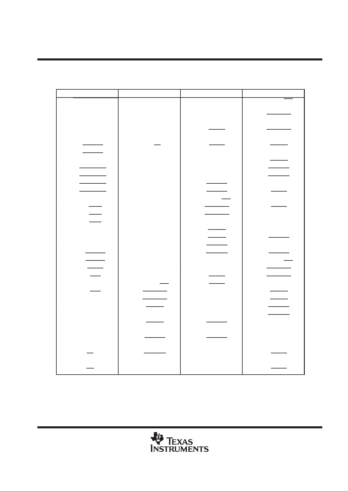
signal names by pin number
Table 4. Signals Sorted Numerically by Pin Number (128-Pin Package)
NO TERMINAL NAME NO TERMINAL NAME NO TERMINAL NAME NO TERMINAL NAME
1 NC 33 NC 65 NC 97 NC
2 ATTN0[3] 34 RSVD 66 RSVD 98 PWRON/OFF[2]
3 ATTN1[3] 35 RSVD 67 RSVD 99 PWRFAULT[2]
4 M66EN[3] 36 RSVD 68 BUSON[0] 100 PWRGOOD[2]
5 DETECT0[3] 37 CS 69 CLKON[0] 101 PRSNT1[2]
6 DETECT1[3] 38 DAT A7 70 ATTN0[0] 102 V
CC
7 V
CC
39 V
CC
71 ATTN1[0] 103 PRSNT2[2]
8 SLOTREQ64[3] 40 DATA6 72 M66EN[0] 104 SLOTRST[2]
9 SLOTREQ64[2 41 DATA5 73 GND 105 REQ64ON[2]
10 SLOTREQ64[1] 42 DATA4 74 DETECT0[0] 106 REQ64ON[2]
11 SLOTREQ64[0] 43 DATA3 75 DETECT1[0] 107 BUSON[2]
12 GND 44 GND 76 PWRON/OFF[1] 108 GND
13 SREQ 45 DATA2 77 PWRFAULT[1] 109 CLKON[2]
14 SGNT 46 DATA1/ADD6 78 PWRGOOD[1] 110 ATTN0[2]
15 PRST 47 DATA0/ADD5 79 V
CC5V
111 ATTN1[2]
16 V
CC5V
48 A4/ADD4 80 PRSNT1[1] 112 M66EN[2]
17 PCLK 49 V
CC5V
81 PRSNT2[1] 113 DETECT0[2]
18 GND 50 A3/ADD3 82 SLOTRST[1] 114 V
CC5V
19 IDLEREQ 51 A2/ADD2 83 REQ64ON[1] 115 DETECT1[2]
20 IDLEGNT 52 A1/ADD1 84 GND 116 PWRON/OFF[3]
21 FRAME 53 A0/ADD0 85 REQ64ON[1] 117 PWRFAULT[3]
22 IRDY 54 GND 86 BUSON[1] 118 PWRGOOD[3]
23 V
CCP
55 PWRON/OFF[0] 87 CLKON[1] 119 GND
24 INTR 56 PWRFAULT[0] 88 ATTN0[1] 120 PRSNT1[3]
25 INTR 57 PWRGOOD[0] 89 ATTN1[1] 121 PRSNT2[3
26 SYSM66EN 58 PRSNT1[0] 90 V
CC
122 SLOTRST[3]
27 GND 59 V
CC
91 M66EN[1] 123 REQ64ON[3]
28 SMODE 60 PRSNT2[0] 92 DETECT0[1] 124 GND
29 V
CC5V
61 SLOTRST[0] 93 DETECT1[1] 125 REQ64ON[3]
30 RD/SDA 62 REQ64ON[0] 94 RSVD 126 BUSON[3]
31 WR/SCL 63 REQ64ON[0] 95 RSVD 127 CLKON[3]
32 NC 64 NC 96 NC 128 NC
Page 10
HPC3130
PCI HOT PLUG CONTROLLER
SCPS029B – DECEMBER1998
10
POST OFFICE BOX 655303 • DALLAS, TEXAS 75265
signal names by terminal name
Table 5. Signals Sorted Alphabetically by Terminal Name (144-Pin Package)
TERMINAL NAME NO TERMINAL NAME NO TERMINAL NAME NO TERMINAL NAME NO
A0/ADD0 59 DETECT1[2] 129 NC 78 REQ64ON[3] 137
A1/ADD1 58 DETECT1[3] 8NC103 REQ64ON[0] 72
A2/ADD2 57 FRAME 23 NC 105 REQ64ON[1] 95
A3/ADD3 56 GND 14 NC 107 REQ64ON[2] 120
A4/ADD4 54 GND 20 NC 110 REQ64ON[3] 140
ATTN0[0] 80 GND 29 NC 112 RSVD 37
ATTN0[1] 98 GND 50 NC 114 RSVD 39
ATTN0[2] 124 GND 60 NC 139 RSVD 41
ATTN0[3] 1 GND 83 NC 141 RSVD 73
ATTN1[0] 81 GND 94 NC 143 RSVD 75
ATTN1[1] 99 GND 122 PCLK 19 RSVD 106
ATTN1[2] 125 GND 133 PRSNT1[0] 64 RSVD 108
ATTN1[3] 3 GND 138 PRSNT1[1] 90 SGNT 16
BUSON[0] 77 IDLEGNT 22 PRSNT1[2] 115 SLOTREQ64[0] 13
BUSON[1] 96 IDLEREQ 21 PRSNT1[3] 134 SLOTREQ64[1] 12
BUSON[2] 121 INTR 27 PRSNT2[0] 66 SLOTREQ64[2] 11
BUSON[3] 142 INTR 26 PRSNT2[1] 91 SLOTREQ64[3] 10
CLKON[0] 79 IRDY 24 PRSNT2[2] 117 SLOTRST[0] 68
CLKON[1] 97 M66EN[0] 82 PRSNT2[3] 135 SLOTRST[1] 92
CLKON[2] 123 M66EN[1] 101 PRST 17 SLOTRST[2] 118
CLKON[3] 144 M66EN[2] 126 PWRFAULT[0] 62 SLOTRST[3] 136
CS 43 M66EN[3] 5 PWRFAULT[1] 87 SMODE 30
DATA0/ADD5 53 NC 2 PWRFAULT[2] 111 SREQ 15
DATA1/ADD6 52 NC 4 PWRFAULT[3] 131 SYSM66EN 28
DATA2 51 NC 6 PWRGOOD[0] 63 V
CC
9
DATA3 49 NC 31 PWRGOOD[1] 88 V
CC
45
DATA4 48 NC 33 PWRGOOD[2] 113 V
CC
65
DATA5 47 NC 35 PWRGOOD[3] 132 V
CC
100
DATA6 46 NC 38 PWRON/OFF[0] 61 V
CC
116
DATA7 44 NC 40 PWRON/OFF[1] 86 V
CC5V
18
DETECT0[0] 84 NC 42 PWRON/OFF[2] 109 V
CC5V
32
DETECT0[1] 102 NC 67 PWRON/OFF[3] 130 V
CC5V
55
DETECT0[2] 127 NC 69 RD/SDA 34 V
CC5V
89
DETECT0[3] 7NC71 REQ64ON[0] 70 V
CC5V
128
DETECT1[0] 85 NC 74 REQ64ON[1] 93 V
CCP
25
DETECT1[1] 104 NC 76 REQ64ON[2] 119 WR/SCL 36
Page 11
HPC3130
PCI HOT PLUG CONTROLLER
SCPS029B – DECEMBER1998
11
POST OFFICE BOX 655303 • DALLAS, TEXAS 75265
signal names by pin number
Table 6. Signals Sorted Numerically by Pin Number (144-Pin Package)
NO TERMINAL NAME NO TERMINAL NAME NO TERMINAL NAME NO TERMINAL NAME
1 ATTN0[3] 37 RSVD 73 RSVD 109 PWRON/OFF[2]
2 NC 38 NC 74 NC 110 NC
3 ATTN1[3] 39 RSVD 75 RSVD 111 PWRFAULT[2]
4 NC 40 NC 76 NC 112 NC
5 M66EN[3] 41 RSVD 77 BUSON[0] 113 PWRGOOD[2]
6 NC 42 NC 78 NC 114 NC
7 DETECT0[3] 43 CS 79 CLKON[0] 115 PRSNT1[2]
8 DETECT1[3] 44 DAT A7 80 ATTN0[0] 116 V
CC
9 V
CC
45 V
CC
81 ATTN1[0] 117 PRSNT2[2]
10 SLOTREQ64[3] 46 DATA6 82 M66EN[0] 118 SLOTRST[2]
11 SLOTREQ64[2] 47 DATA5 83 GND 119 REQ64ON[2]
12 SLOTREQ64[1] 48 DATA4 84 DETECT0[0] 120 REQ64ON[2]
13 SLOTREQ64[0] 49 DATA3 85 DETECT1[0] 121 BUSON[2]
14 GND 50 GND 86 PWRON/OFF[1] 122 GND
15 SREQ 51 DATA2 87 PWRFAULT[1] 123 CLKON[2]
16 SGNT 52 DATA1/ADD6 88 PWRGOOD[1] 124 ATTN0[2]
17 PRST 53 DATA0/ADD5 89 V
CC5V
125 ATTN1[2]
18 V
CC5V
54 A4/ADD4 90 PRSNT1[1] 126 M66EN[2]
19 PCLK 55 V
CC5V
91 PRSNT2[1] 127 DETECT0[2]
20 GND 56 A3/ADD3 92 SLOTRST[1] 128 V
CC5V
21 IDLEREQ 57 A2/ADD2 93 REQ64ON[1] 129 DETECT1[2]
22 IDLEGNT 58 A1/ADD1 94 GND 130 PWRON/OFF[3]
23 FRAME 59 A0/ADD0 95 REQ64ON[1] 131 PWRFAULT[3]
24 IRDY 60 GND 96 BUSON[1] 132 PWRGOOD[3]
25 V
CCP
61 PWRON/OFF[0] 97 CLKON[1] 133 GND
26 INTR 62 PWRFAULT[0] 98 ATTN0[1] 134 PRSNT1[3]
27 INTR 63 PWRGOOD[0] 99 ATTN1[1] 135 PRSNT2[3]
28 SYSM66EN 64 PRSNT1[0] 100 V
CC
136 SLOTRST[3]
29 GND 65 V
CC
101 M66EN[1] 137 REQ64ON[3]
30 SMODE 66 PRSNT2[0] 102 DETECT0[1] 138 GND
31 NC 67 NC 103 NC 139 NC
32 V
CC5V
68 SLOTRST[0] 104 DETECT1[1] 140 REQ64ON[3]
33 NC 69 NC 105 NC 141 NC
34 RD/SDA 70 REQ64ON[0] 106 RSVD 142 BUSON[3]
35 NC 71 NC 107 NC 143 NC
36 WR/SCL 72 REQ64ON[0] 108 RSVD 144 CLKON[3]
Page 12
HPC3130
PCI HOT PLUG CONTROLLER
SCPS029B – DECEMBER1998
12
POST OFFICE BOX 655303 • DALLAS, TEXAS 75265
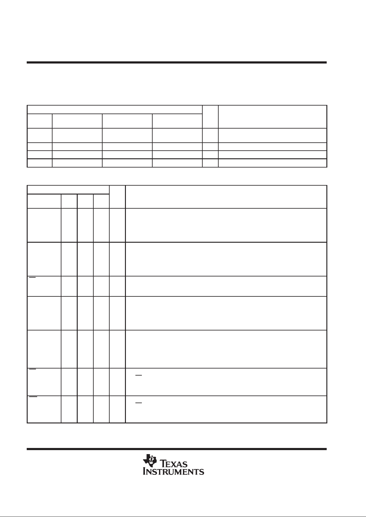
Terminal Functions
This section describes the HPC3130 terminal functions. The terminals are grouped in tables by function.
power supply terminal functions
TERMINAL
NAME
NO.
120
NO.
128
NO.
144
I/O FUNCTION
GND 11, 17, 26, 41, 51,
68, 79, 101, 112, 117
12, 18, 27, 44, 54,
73, 84, 108, 119, 124
14, 20, 29, 50, 60,
83, 94, 122, 133, 138
I Device ground terminals
V
CC
6, 36, 56, 85, 95 7, 39, 59, 90, 102 9, 45, 65, 100, 116 I 3.3-V power supply
V
CC5V
15, 28, 46, 74, 107 16, 29, 49, 79, 114 18, 32, 55, 89, 128 I 5-V clamp-rail voltage supply
V
CCP
22 23 25 I Clamp rail voltage for PCI signaling (5V or 3.3V)
control bus interface
TERMINAL
NAME
NO.
120
NO.
128
NO.
144
I/O FUNCTION
A2/ADD2
A1/ADD1
A0/ADD0
48
49
50
51
52
53
57
58
59
I Parallel bus address. These terminals are address inputs in generic parallel bus cycles and are
only used when the SMODE is input low. These lower address terminals select one of the eight
registers for read/write access.
Serial bus address select. These terminals indicate the full serial bus address of the HPC3130
when the SMODE is input high.
A4/ADD4
A3/ADD3
4547485054
56
I Parallel bus address. These terminals are address inputs in generic parallel bus cycles, and are
only used when SMODE is input low. These upper address terminals select one of four hot-plug
slots supported by the HPC3130.
Serial bus address select. These terminals indicate the full serial bus address of the HPC3130
when the SMODE is input high.
CS 34 37 43 I Chip selection. This active low input selects the HPC3130 chip as addressed in the current
generic parallel bus cycle. This chip input is only valid if the SMODE is input low. Multiple
HPC3130 chips may exist in a system with external logic driving this signal.
DATA1/ADD6
DATA0/ADD5434446475253
I/O Parallel bus data. This bus is the data bus in generic parallel bus cycles and is selected when the
SMODE is input low. The data path is used during both read and write transactions to internal
registers when the parallel control bus interface is implemented.
Serial bus address selection. These terminals indicate the full serial bus address of the
HPC3130 when the SMODE is input high.
DATA7
DATA6
DATA5
DATA4
DATA3
DATA2
35
37
38
39
40
42
38
40
41
42
43
45
44
46
47
48
49
51
I/O Parallel bus data. This bus is the data bus in generic parallel bus cycles and is selected when the
SMODE is input low. The data path is used during both read and write transactions to internal
registers when the parallel control bus interface is implemented.
RD/SDA 29 30 34 I/O Read selection. This terminal indicates a register read cycle when the SMODE input is low and
the CS
terminal input is asserted. This is used to read an internal HPC3130 register.
Serial bus data. This terminal signals the serial bus data when the SMODE input is high. It is used
during internal register read and write transactions.
WR/SCL 30 31 36 I Write selection. This terminal indicates a register write cycle when the SMODE input is low and
the CS
terminal input is asserted. This input is used to write to an internal HPC3130 register.
Serial bus clock. This terminal inputs serial bus clock in when the SMODE input is high. It is used
during internal register read and write transactions.
Page 13

HPC3130
PCI HOT PLUG CONTROLLER
SCPS029B – DECEMBER1998
13
POST OFFICE BOX 655303 • DALLAS, TEXAS 75265
Terminal Functions (Continued)
system interface
TERMINAL
NAME
NO.
120
NO.
128
NO.
144
I/O FUNCTION
FRAME 20 21 23 I Frame. This input and the IRDY input indicate that the PCI bus is idle. When the HPC3130
senses the PCI bus is idle after IDLEGNT
is low, a hot-plug slot can be connected to the PCI
bus. This input must be wired to a valid logic level if the bus idling procedure is not implemented.
IDLEGNT 19 20 22 I Idle grant. This input indicates when the PCI bus is idled by the HOST-PCI bridge after a
request is made by IDLEREQ
. The protocol is identical to PCI request/grant. This input must be
wired to a valid logic level if the bus idling procedure is not implemented.
IDLEREQ 18 19 21 O Idle request. This output is driven to request the HOST -PCI bridge to idle the PCI bus before
connecting a hot-plug slot. The protocol is identical to PCI request/grant. A pullup resistor must
be implemented on this terminal if the bus idling procedure is not implemented.
INTR 24 25 27 O System interrupt. This output provides a system interrupt. The HPC3130 can be programmed
to assert this interrupt under various conditions, which may be serviced by the hot-plug service.
Furthermore, the event status/enable state is compliant with the
ACPI Specification
and, as a
result, supports ACPI control methods for switching the HPC3130.
INTR 23 24 26 O System interrupt. This open drain output provides a system interrupt. The HPC3130 can be
programmed to assert this interrupt under various conditions, which may be serviced by the
hot-plug. Furthermore, the event status/enable state is compliant with the
ACPI Specification
and, as a result, supports ACPI control methods for switching the HPC3130.
IRDY 21 22 24 I Initiator ready . This and the FRAME input indicate that the PCI bus is idle. When the HPC3130
senses the PCI bus is idle after IDLEGNT
is low, a hot-plug slot may be connected to the PCI
bus. This input must be wired to a valid logic level if the bus idling procedure is not implemented.
PCLK 16 17 19 I PCI clock input. These terminals provide the PCI clock to the HPC3130, which uses it only for
activity indicator timing, IDLEREQ
/IDLEGNT protocol, and connection sequencing.
PRST 14 15 17 I PCI reset. This signal provides the PCI reset to the HPC3130. After a PCI reset, the HPC3130
resides in a state where all slots are enabled, as in a non-hot-plug system. The HPC3130
passes PCI resets from the host to all hot-plug slots.
SGNT 13 14 16 O Secondary grant. This output provides a scheme to cascade a secondary HPC3130 device in
order to provide more than four slots. The SGNT
output from the primary HPC3130 is input to
the IDLEGNT
terminal for the secondary HPC3130. After the secondary HPC3130 requests
the primary HPC3130 to idle the bus, the primary HPC3130 arbitrates for the bus using
IDLEREQ
. Once IDLEGNT is asserted, the primary HPC3130 asserts its SGNT output. This
indicates to the secondary HPC3130 device that it can connect to the bus.
SMODE 27 28 30 I Serial bus mode. When this input is asserted high, the internal HPC3130 registers are
accessible through serial bus interface; otherwise, they are accessed through the generic
parallel bus interface. This input selects the control bus interface.
SREQ 12 13 15 I Secondary request. This input provides a scheme to cascade a second HPC3130 device in
order to provide more than four slots. The IDLEREQ
from the second HPC3130 device is input
to the SREQ
terminal of the primary HPC3130. If the second HPC3130 device arbitrates for the
bus by asserting its IDLEREQ
output, this scheme causes the primary HPC3130 to assert its
IDLEREQ
. If cascading is not used, this input is pulled high.
SYSM66EN 25 26 28 I/O PCI bus frequency indicator. This signal indicates the PCI clock frequency requirements of the
hot-plug slots, and must be tied to the system PCI bus M66EN signal. The output from this
terminal only changes state after a PCI reset and is only required in a 66-MHz system.
Page 14

HPC3130
PCI HOT PLUG CONTROLLER
SCPS029B – DECEMBER1998
14
POST OFFICE BOX 655303 • DALLAS, TEXAS 75265
Terminal Functions (Continued)
slot control and status functions
TERMINAL
NAME
NO.
120
NO.
128
NO.
144
I/O FUNCTION
ATTN0[3]
ATTN0[2]
ATTN0[1]
ATTN0[0]
ATTN1[3]
ATTN1[2]
ATTN1[1]
ATTN1[0]
1
103
83
65
2
104
84
66
2
110
88
70
3
111
89
71
1
124
98
80
3
125
99
81
O Attention indicators. These two outputs are provided per slot as attention indicators and can
be independently programmed to drive high, low, fast blink, and slow blink. The timer is
based on the PCI clock frequency and the state of SYSM66EN.
BUSON[3]
BUSON
[2]
BUSON
[1]
BUSON
[0]
119
100
81
63
126
107
86
68
142
121
96
77
O CBT switch control for PCI bus. This output controls the CBT switch that connects the
hot-plug slot to the system PCI bus. This output is only driven by the HPC3130 under
programmed control.
CLKON[3]
CLKON
[2]
CLKON
[1]
CLKON
[0]
120
102
82
64
127
109
87
69
144
123
97
79
O PCI clock connection control. This output is used to control the CBT switch or clock driver
that connects the hot-plug slot to the system PCI clock. This output is only driven by the
HPC3130 under programmed control.
DETECT0[3]
DETECT0
[2]
DETECT0
[1]
DETECT0
[0]
DETECT1
[3]
DETECT1
[2]
DETECT1
[1]
DETECT1
[0]
4
106
87
69
5
108
88
70
5
113
92
74
6
115
93
75
7
127
102
84
8
129
104
85
I Card detection signals. These two card detect input signals, DETECT0 and DETECT1, are
provided as additional card detection signals to the PRSNT1
and PRSNT2. Since only one
present input must be tied to ground to indicate a card is present per the
PCI Specification
,
these optional inputs are provided for designers of a more mechanically robust system. If the
protection enable bit is set to 1 in the general configuration register, the HPC3130 does not
power a hot-plug slot unless DETECT0
and DETECT1 are input low. A design not
implementing additional card detection must tie these signals to ground. When this feature is
utilized, the HPC3130 guarantees that power can not be applied to an empty slot or a slot
with a partially inserted card.
M66EN[3]
M66EN[2]
M66EN[1]
M66EN[0]
3
105
86
67
4
112
91
72
5
126
101
82
I/O PCI bus frequency indicator. This signal indicates the PCI clock frequency requirements of
the hot-plug slots and is only required in a 66-MHz system (two slot maximum electrical
loading limits). The two slot interfaces that provide the M66EN terminals are sensed at PCI
reset and are driven afterwards.
PRSNT1[3]
PRSNT1
[2]
PRSNT1
[1]
PRSNT1
[0]
PRSNT2
[3]
PRSNT2
[2]
PRSNT2
[1]
PRSNT2
[0]
113
94
75
55
114
96
76
57
120
101
80
58
121
103
81
60
134
115
90
64
135
117
91
66
I Present signals. These inputs are provided by hot-plug slots to indicate that an add-in card is
physically present in the slot and to power requirements to the system. Only one of these
signals must be tied to ground to indicate a card is present in an expansion slot. A set of
PRSNT1
and PRSNT2 inputs are provided for each hot-plug slot.
PWRFAULT[3]
PWRFAULT
[2]
PWRFAULT
[1]
PWRFAULT
[0]
110
92
72
53
117
99
77
56
131
111
87
62
I Power fault. This input is provided per slot power switch to indicate if there is a power fault.
The HPC3130 can be programmed to generate an interrupt through INTR
when this input is
asserted.
PWRGOOD[3]
PWRGOOD
[2]
PWRGOOD
[1]
PWRGOOD
[0]
111
93
73
54
118
100
78
57
132
113
88
63
I Power good. This input is provided per slot power switch to indicate when power is
successfully switched. The HPC3130 can be programmed to generate an interrupt through
INTR
when this input is asserted.
Page 15

HPC3130
PCI HOT PLUG CONTROLLER
SCPS029B – DECEMBER1998
15
POST OFFICE BOX 655303 • DALLAS, TEXAS 75265
Terminal Functions (Continued)
slot control and status functions (continued)
TERMINAL
NAME
NO.
120
NO.
128
NO.
144
I/O FUNCTION
PWRON/OFF[3]
PWRON/OFF
[2]
PWRON/OFF
[1]
PWRON/OFF
[0]
109
91
71
52
116
98
76
55
130
109
86
61
O Power ON/OFF . This output is provided per slot and is driven to the power switch to control
the slot power state.
REQ64ON[3]
REQ64ON
[2]
REQ64ON
[1]
REQ64ON
[0]
116
98
78
59
123
105
83
62
137
119
93
70
O CBT switch control for SLOTREQ64. A CBT switch can be implemented to reduce trace
loading of the additional REQ64
signal inherent to the HPC3130 controller. This output can
be used to control the CBT switch. This output is only driven by the HPC3130 under
programmed control.
REQ64ON[3]
REQ64ON[2]
REQ64ON[1]
REQ64ON[0]
118
99
80
60
125
106
85
63
140
120
95
72
O CBT switch control for SLOTREQ64. A CBT switch can be implemented to reduce trace
loading of the additional REQ64
signal inherent to the HPC3130 controller. This output can
be used to control the CBT switch. This output is only driven by the HPC3130 under
programmed control.
SLOTREQ64[3]
SLOTREQ64
[2]
SLOTREQ64
[1]
SLOTREQ64
[0]
7
8
9
10
8
9
10
11
10
11
12
13
O Slot request 64. This output is driven in conjunction with SLOTRST to the hot-plug slot to
indicate to option cards whether or not they are plugged into a 64-bit slot. If a 64-bit device
is plugged into a 32-bit slot, then it must ensure that its high-word path inputs do not
oscillate and that there is not a significant power drain through the input buffer. This output
is only driven by the HPC3130 under programmed control.
SLOTRST[3]
SLOTRST
[2]
SLOTRST
[1]
SLOTRST
[0]
115
97
77
58
122
104
82
61
136
118
92
68
O Slot PCI reset. This output is driven to the hot-plug slot to reset it after power up. When a
card is inserted into a hot-plug slot it must be reset independent of the other PCI devices on
the bus. This output is only driven by the HPC3130 under programmed control.
HPC3130 applications
This section discusses the various features of the HPC3130 in detail, and presents design considerations
including a general connection sequencing guideline.
system implementation
Figure 1 illustrates the HPC3130 implementation. The PCI bus signals are switched to the hot–plug PCI slot
by the BUSON
output, which controls a CBT switch. The PCI clock, PCI reset, M66EN, and REQ64 must not
be routed through the CBT switch. The HPC3130 drives the slot PCI reset and SLOTREQ64
, which can be
controlled by internal HPC3130 registers. The SLOTREQ64
requires special consideration during reset, as
described. The PCI clock to the slot is driven by a clock driver, which is enabled by the HPC3130 CLKON
output.
The HPC3130 also provides other features such as mechanical detection circuits, attention indicators, and
interrupt signaling. The mechanical detection circuitry using the DETECT[1,0]
inputs is displayed as a dotted
line and is an optional feature. Two attention indicator outputs, ATTN[1,0], are provided: one indicator to draw
the attention of the user to a particular slot for insertion/removal, and one optional indicator that can be used
to indicate fault conditions. Additional features, such as 66-MHz capability and automatic sequencing, are
discussed in the following sections.
Page 16

HPC3130
PCI HOT PLUG CONTROLLER
SCPS029B – DECEMBER1998
16
POST OFFICE BOX 655303 • DALLAS, TEXAS 75265
8–BIT
PORT
HOST/PCI
INTR
PCLK
PRST
SYSM66EN
BUSON CBT–SW
CBT–SW
CLKON
CBT–SW
REQ64ON
SLOTREQ64
M66EN
PRSNT
(1–2)
P
C
I
S
L
O
T
SLOTRST
PWRON/OFF
PERFAULT
PWRGOOD
PWR–SW
DETECT(0–1)
ATTN(0–1)
FRAME
IRDY
IDLEREQ
IDLEGNT
HPC–PCI
PCI Bus
PCI Bus Less PRST
and REQ64
Motherboard
PCI Device
Figure 1. HPC3130 Implementation
The HPC3130 internal registers can be accessed through either a two-wire serial interface or an 8-bit generic
parallel bus (ISA-like). The above figure illustrates the 8-bit port configuration. Not shown in the diagram is the
SMODE chip input that must be wired low to indicate parallel bus interface mode. Also not shown in the diagram
is the external chip-select logic required to select the HPC3130 in ISA bus cycles.
serial interface
The internal registers can be accessed either through a two-wire serial interface or through an 8-bit generic
parallel interface. The SMODE input selects one of these modes.
The HPC3130 implements a two-pin serial slave interface with one clock signal (SCL) and one data signal
(SDA). This serial interface can operate with a serial clock frequency up to 400 kHz. Both SCL and SDA require
pullup resistors for the serial slave interface to function properly.
All data transfers are initiated by the serial bus master. The beginning of a data transfer is indicated by a ST AR T
condition (S) when the SDA line transitions to a low state while SCL is in a high state as illustrated in Figure 2.
The end of a requested data transfer is indicated by a STOP condition (P), which is the low-to-high transition
of SDA while SCL is in the high state. Data on SDA must remain stable during the high state of the SCL signal.
Changes on the SDA signal during the high state of SCL will be interpreted as control signals, that is, a ST ART
or STOP condition.
The SCL is an input into the HPC3130 and SDA is bidirectional.
Page 17

HPC3130
PCI HOT PLUG CONTROLLER
SCPS029B – DECEMBER1998
17
POST OFFICE BOX 655303 • DALLAS, TEXAS 75265
SDA
SCL
Start Condition Stop Condition
Change of
Data Allowed
Data Line Stable, Data Valid
Figure 2. Serial Bus Start/Stop Conditions and Bit Transfers
Data is transferred on the bus in 8-bit bytes. The number of bytes that can be transmitted during a data transfer
is unlimited; however, each byte must be completed with an acknowledge bit. An acknowledge (ACK) is
indicated by the receiver pulling down the SDA signal so that it remains low during the high state of the SCL
signal as shown in Figure 3.
SCL From
Master
123 789
SDA Output
By Transmitter
SDA Output
By Receiver
Figure 3. Serial Bus Protocol – Acknowledge
The HPC3130 serial bus slave interface protocol for write transactions is illustrated in Figure 4. The R/W
command bit is set to zero to indicate a write transaction. For a write operation, the HPC3130 requires a word
address field after the slave address. This address field is comprised of eight bits. Upon receipt of the word
address, the HPC3130 responds with an acknowledge, and waits for the next eight bits of data, again
responding with an acknowledge. After all the data bytes are transferred, the master then terminates the transfer
by generating a STOP condition. The device automatically increments the address for subsequent data words.
After the receipt of each word, the low order address bits are internally incremented by one.
Sb6 b4b5 b3 b2 b1 b0 0 b7 b6 b5 b4 b3 b2 b1 b0AA
Slave Address Word Address
R/W
S/P = Start/stop conditionA = Slave acknowledgment
b7 b6 b4b5 b3 b2 b1 b0 A P
Data Byte
Figure 4. Serial Bus Protocol – Byte Write
A byte read operation is illustrated below. The read protocol is very similar to the write protocol, except the R/W
command bit must be set to one to indicate a read data transfer. First the master issues a write command that
includes the ST ART condition and the slave address field (with the R/W
bit set to write), followed by the address
of the word it is to read. This procedure sets the internal address counter of the HPC3130 to the desired address.
After the word address acknowledgment is received by the master, the master immediately reissues a START
condition followed by another slave address field with the R/W
bit set to read. The HPC3130 responds with an
acknowledgment and transmits the eight data bits stored in the addressed location. If the master responds with
Page 18

HPC3130
PCI HOT PLUG CONTROLLER
SCPS029B – DECEMBER1998
18
POST OFFICE BOX 655303 • DALLAS, TEXAS 75265
an acknowledge signal, indicating that it requires additional data, the HPC3130 continues to output data for each
received acknowledge signal. The master terminates the sequential read operation by not responding with an
acknowledge signal, and issues a STOP condition.
b7Sb6 b4b5 b3 b2 b1 b0 0 b7 b6 b5 b4 b3 b2 b1 b0AA
Slave Address Word Address
R/W
S/P = Start/stop conditionA = Slave acknowledgment
b6 b4b5 b3 b2 b1 b0 1 A
Data Byte
M = Master acknowledgment
S b6 b4b5 b3 b2 b1 b0 M Pb6 b4b5 b3 b2 b1 b0 M P
Slave Address
R/WRestart StopStart
Figure 5. Serial Bus Protocol – Byte Read
parallel interface
The HPC3130 also implements an 8-bit parallel interface mode. When this mode is selected, the HPC3130
internal register addressed by the A[4:0] inputs can be accessed for a read/write transaction using the CS
, RD,
WR
strobes. The following signals have pullups on the mother board: IO16, M16, NOWS, CHRDY, MEMR,
MEMW
, IOR, IOW, SD[15:0] to implement default states. Figure 6 shows write access using the default 8-bit
standard ISA bus cycle with four wait states. A read cycle is similar.
BCLK
CS
WR
A(0–4)
D(0–7)
Figure 6. Parallel Bus Write Cycle
connection sequencing
Before an add-in card is hot plugged and made available to the slot, the various pins in the HPC3130 have to
be controlled in a specific sequence. The HPC3130 provides the software interface to sequence the power to
the slot, clocks, and signals to the add-in cards that are being live inserted. The switch-timing block is used to
control the exact timing when the CBT switches are enabled.
The initial software sequencing is done by setting individual bits in the hot plug control register in the following
sequence. First, the SL TPWR_CTL bit is set high to drive the PWRON/OFF
signal high. After the power to the
slot is applied, the SLOTRST_O bit is set low to drive the SLOTRST
output. Next the CLKON_O bit is set low
to enable the PCI clock to the slot. Also, the REQ64_O bit is set to a value of 0 and the SLOTREQ64 bit is set
to indicate to the add-in card whether it is inserted into a 64-bit or 32-bit slot. SLOTREQ64 is set low for a 64-bit
slot and is set high for a 32-bit slot.
After initial software sequencing of the above signals is complete, the next step is to enable the CBT switches.
This can be done either by using the software to manually set the BUS_CTL bit or using the HPC3130 via the
automatic connection sequence mode located in the general configuration register.
Page 19
HPC3130
PCI HOT PLUG CONTROLLER
SCPS029B – DECEMBER1998
19
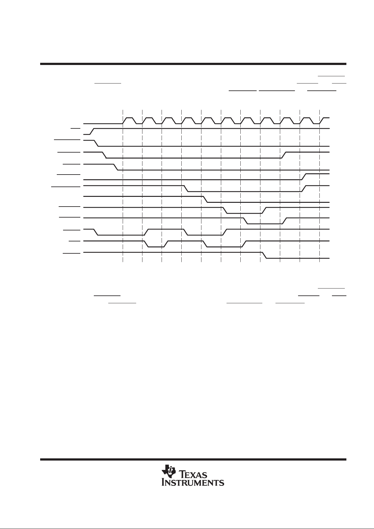
POST OFFICE BOX 655303 • DALLAS, TEXAS 75265
If automatic sequencing mode 1 is selected, then the BUS_CTL bit controls the sequencing by using idling
protocol. When this bit is set to zero, the switch–timing block will arbitrate for the PCI Bus by asserting IDLEREQ
.
Subsequently, IDLEGNT
is asserted and the HPC3130 waits for bus idle condition. When FRAME and IRDY
are deasserted, the CBT switches are enabled. Following this, the SLOTRST , SLOTREQ64 and REQ64ON are
deasserted. Figure 7 depicts the sequencing of events when automatic sequencing mode 1 is enabled.
PCI_CLK
PWRON/OFF
PWRGOOD
SLOTRST
CLKON
REQ64ON
SLOTREQ64
BUS_CTL
IDLEREQ
IDLEGNT
FRAME
IRDY
BUSON
Figure 7. Automatic Connection Sequencing Mode 1
If automatic sequencing mode 2 is selected, then the BUS_CTL bit controls the sequencing by using idling
protocol. When this bit is set to zero, the switch timing block arbitrates for the PCI bus by asserting IDLEREQ
.
Subsequently , IDLEGNT
is asserted and the HPC3130 waits for the bus idle condition. When FRAME and IRDY
are deasserted, the SLOTRST is deasserted. Following this, the SLOTREQ64 and REQ64ON are deasserted
and the CBT switches are enabled. Figure 8 depicts the sequencing of events when automatic sequencing
mode 2 is enabled.
Page 20

HPC3130
PCI HOT PLUG CONTROLLER
SCPS029B – DECEMBER1998
20
POST OFFICE BOX 655303 • DALLAS, TEXAS 75265
PCI_CLK
PWRON/OFF
PWRGOOD
SLOTRST
CLKON
REQ64ON
SLOTREQ64
BUS_CTL
IDLEREQ
IDLEGNT
FRAME
IRDY
BUSON
Figure 8. Automatic Connection Sequencing Mode 2
The protocol described above is identical to the PCI REQ
/GNT protocol used by PCI bus masters, which also
must wait for bus idle through PCI FRAME
and IRDY before initiating a PCI cycle. If the HPC3130 is connected
to PCI FRAME
and IRDY, the HPC3130 arbitrates for the bus; although it does not drive the PCI bus or assert
FRAME
to start a cycle.
There are some issues with this implementation such as bus parking and additional loading on the PCI FRAME
and IRDY signals, which need to be considered when designing a system. The system designer may have a
level of confidence that PCI adapter cards can tolerate connection to a non-idle bus. In the scenario where the
HPC3130 is not connected to the bus, then the FRAME
, IRDY , and IDLEGNT must be wired to valid logic levels
and the automatic sequencing will start without any relationship to the bus.
Page 21

HPC3130
PCI HOT PLUG CONTROLLER
SCPS029B – DECEMBER1998
21
POST OFFICE BOX 655303 • DALLAS, TEXAS 75265
IDLEREQ, IDLEGNT , FRAME, and IRDY pins are not connected in manual mode. In contrast, during automatic
connection, the HPC3130 requests the PCIBus to make sure it is idle before it sequences through the
connection sequence.
In manual mode, software has to perform each part of the connection sequence. Figure 9 is an example of the
manual connection sequence. There could be several other ways to implement this protocol.
PCI_CLK
PWRON/OFF
PWRGOOD
SLOTRST
CLKON
REQ64ON
SLOTREQ64
BUS_CTL
BUSON
Figure 9. Manual Connection Sequencing
disconnecting sequence
The HPC3130 provides two mechanisms to isolate a PCI slot from the PCI bus so an add–in card can be
removed. One of the mechanisms is called manual sequencing and is enabled by default. This mechanism
allows the software to control the entire disconnect sequence. This means it is the software’s responsibility to
remove a powered slot from the PCI bus without any impact to the system.
The second mechanism is called auto sequencing and can be enabled by programming either Auto-Sequence
1 or Auto-Sequence 2 in the general configuration register
.
Unlike the connection sequence, which has two
different auto-connection sequencing modes, the autodisconnect sequence has only one mode of operation.
The steps in the auto-disconnect sequence are as follows:
1. Software may assert SLOTRST
to the appropriate slot by writing a 0 to the SLOTRST_O bit in the hot-plug
control register. This is optional.
2. Next the software must set the BUS_CTL bit in the hot-plug control register to a 1.
3. Once the BUS_CTL bit is set to a 1, the HPC3130 asserts IDLEREQ
.
4. Once IDLEGNT
is asserted and FRAME and IRDY are deasserted, the HPC3130 deasserts BUSON and
CLKON
and asserts REQ64ON to isolate the slot from the PCI bus.
5. The HPC3130 then drives PWRON/OFF
low to power off the slot.
Page 22

HPC3130
PCI HOT PLUG CONTROLLER
SCPS029B – DECEMBER1998
22
POST OFFICE BOX 655303 • DALLAS, TEXAS 75265
PCI_CLK
PWRON/OFF
PWRGOOD
SLOTRST
CLKON
REQ64ON
SLOTREQ64
BUS_CTL
IDLEREQ
IDLEGNT
FRAME
IRDY
BUSON
Figure 10. Automatic Disconnect Sequencing Mode
In manual disconnect mode, software has to perform each part of the disconnection sequence. Figure 1 1 is an
example of the manual disconnection sequence. There could be several other ways to implement this protocol.
During the manual disconnection, PCIBus may or may not idle; it will depend on the software implementation
of the system.
PCI_CLK
PWRON/OFF
PWRGOOD
SLOTRST
CLKON
REQ64ON
SLOTREQ64
BUS_CTL
BUSON
Figure 11. Manual Disconnect Sequencing Mode
Page 23
HPC3130
PCI HOT PLUG CONTROLLER
SCPS029B – DECEMBER1998
23
POST OFFICE BOX 655303 • DALLAS, TEXAS 75265
SLOTREQ64
The SLOTREQ64 signal must be driven by the HPC3130 during reset of a hot-plug slot. The REQ64 signal must
also be driven by the system PCI bus. This requirement can be implemented using the HPC3130 and the
CBT3306 switch or the CBT3257 switch, as shown in Figures 12 and 13. The PCI REQ64
signal must not pass
through the PCI bus CBT switch controlled by BUSON
for this implementation. In a 32-bit PCI bus
implementation, the SLOTREQ64
, REQ64ON and RFQ64ON outputs are not connected to any device.
HPC_PCI
BUSON
System PCI Bus
REQ64ON
SYSTEMREQ64
REQ64ON
SLOTREQ64
CBT3306
PCI
SLOT
Figure 12. SLOTREQ64 Implementation Using CBT3306
HPC_PCI
BUSON
System PCI Bus
SYSTEMREQ64
REQ64ON
SLOTREQ64
CBT3257
S OE
PCI
SLOT
Figure 13. SLOTREQ64 Implementation Using CBT3257
Page 24

HPC3130
PCI HOT PLUG CONTROLLER
SCPS029B – DECEMBER1998
24
POST OFFICE BOX 655303 • DALLAS, TEXAS 75265
66-MHz PCI support
The HPC3130 supports up to two slots in a 66-MHz system: slot 0 and slot 1. These hot-plug slot interfaces
include the M66EN signal and the SYSM66EN signal communicates hot-plug slot capability to the system.
Figure 14 illustrates the 66-MHz support function in the HPC3130.
HPC–PCI M66EN FUNCTION
33 MHz
SYSM66EN
PCLK DRIVER
CB1G1257
PCI
SLOT
System PCI Bus
Motherboard
PCI Device
66 MHz
CLKON 0 PRST
CO
P
M66EN_0
M66EN_I
C
Figure 14. HPC3130 66-MHz System Support
Upon reset, the PCIRST
signal is asserted and the bussed system M66EN signal is latched and selects the
system frequency.
Before an adapter card can be inserted, the slot is prepared for insertion by deasserting BUSON
, deasserting
CLKON
, and powering down the slot. When an adapter card is inserted into either hot-plug slot 0 or slot 1, the
value M66EN from the card can be read through internal registers. If the bus is operating at 66-MHz and a
33-MHz adapter card is inserted, then the software ensures that the card is never connected to the bus. If the
bus is operating at 33 MHz and a 66-MHz adapter card is inserted, then the latched SYSM66EN state can be
driven to the slot by enabling the CBT switch using CLKON
.
SYSM66EN and CLKON
input to a clock driver circuit to control the PCI clock frequency . The 66-MHz support
designed into the HPC3130 allows option cards to indicate PCI clock frequency capabilities upon PCI reset;
however, does not allow an inserted hot-plug card to alter the clock frequency of an operating PCI bus.
Page 25

HPC3130
PCI HOT PLUG CONTROLLER
SCPS029B – DECEMBER1998
25
POST OFFICE BOX 655303 • DALLAS, TEXAS 75265
configuration and control registers
The HPC3130 register set is accessible through either a generic parallel bus interface or a two-wire serial
interface. Eight bytes of register space are provided per slot. Since the HPC3130 supports four slots, a total of
32 bytes of registers is implemented. Register and bit descriptions are provided in the following sections and
indicate the bits that are common to all slots. The bit default values are given, which represent the state of the
HPC3130 after a PCI reset event. After a PCI reset, the HPC3130 drives outputs to a state such that the slots
appear as if they were not a hot-plug platform.
The register map that follows provides the register overview. Byte addressing is required when accessing the
internal registers. Read transactions from reserved registers return zeros.
Table 7. Register Map
SLOT REGISTER NAME ADDRESS SLOT REGISTER NAME ADDRESS
Slot 0 General configuration register 0x00 Slot 2 General configuration register 0x10
Slot 0 Hot-plug slot status register 0x01 Slot 2 Hot-plug slot status register 0x11
Slot 0 Hot-plug slot control register 0x02 Slot 2 Hot-plug slot control register 0x12
Slot 0 Attention indicator control 0x03 Slot 2 Attention indicator control 0x13
Slot 0 Reserved 0x04 Slot 2 Reserved 0x14
Slot 0 Reserved 0x05 Slot 2 Reserved 0x15
Slot 0 Interrupt event status register 0x06 Slot 2 Interrupt event status register 0x16
Slot 0 Interrupt event enable register 0x07 Slot 2 Interrupt event enable register 0x17
Slot 1 General configuration register 0x08 Slot 3 General configuration register 0x18
Slot 1 Hot-plug slot status register 0x09 Slot 3 Hot-plug slot status register 0x19
Slot 1 Hot-plug slot control register 0x0A Slot 3 Hot-plug slot control register 0x1A
Slot 1 Attention indicator control 0x0B Slot 3 Attention indicator control 0x1B
Slot 1 Reserved 0x0C Slot 3 Reserved 0x1C
Slot 1 Reserved 0x0D Slot 3 Reserved 0x1D
Slot 1 Interrupt event status register 0x0E Slot 3 Interrupt event status register 0x1E
Slot 1 Interrupt event enable register 0x0F Slot 3 Interrupt event enable register 0x1F
Page 26

HPC3130
PCI HOT PLUG CONTROLLER
SCPS029B – DECEMBER1998
26
POST OFFICE BOX 655303 • DALLAS, TEXAS 75265
general configuration register
Bit 7 6 5 4 3 2 1 0
Name General configuration register
Type R R R R R/W R/W R R/W
Default 0 0 0 1 0 0 X 0
Register: General configuration
Type: Read-only , Read/Write
Offset: 00h (slot 0), 08h (slot 1), 10h (slot 2), 18h (slot 3)
Default: 0Xh
Description: This register is for general configurations and indications. The automatic PCI bus
connection sequencing is enabled through this register, and the register access mode is
indicated. This register is shared among all four slots.
Table 8. General Configuration Register
BIT TYPE NAME FUNCTION
7–4 R RSVD Reserved for revision ID. These bits return 0001 for this device.
3–2 R/W SEQUENCING Automatic PCI bus connection sequencing. These bits control the sequencing used to connect the hot-
plug slot to the PCI bus.
00 = Manual sequencing through register accesses
01 = Auto–Sequence 1: Enable CBT switches before deasserting RST
10 = Auto–Sequence 2: Enable CBT switches after deasserting RST
11 = Reserved
1 R SYSM66STAT Status of SYSM66EN. This bit represents the latched value of SYSM66EN during a PCI reset. A value of
1 indicates the PCI bus is operating at a frequency greater than 33 MHz. A value of 0 indicates the PCI
bus is operating at 33 MHz or less.
0 R/W PROTECTEN Protection enable. This bit enables a protection mechanism provided by the HPC3130. When this bit is
enabled and either of the DETECT[1:0]
inputs are high, the HPC3130 drives the BUS_ON and CLKON
outputs high. The HPC3130 also drives PWRON/OFF and REQ64ON outputs low.
Page 27

HPC3130
PCI HOT PLUG CONTROLLER
SCPS029B – DECEMBER1998
27
POST OFFICE BOX 655303 • DALLAS, TEXAS 75265
hot-plug slot status register
Bit 7 6 5 4 3 2 1 0
Name Hot-plug slot status register
Type R R R R R R R R
Default X X X X X X X X
Register: Hot-plug slot status
Type: Read-only
Offset: 01h (slot 0), 09h (slot 1), 11h (slot 2), 19h (slot 3)
Default: XXh
Description: This register reports card detection, power status, and other chip input from the hot-plug
slot interface. All bits in this register are read only, and the data read from each bit
represents the logical value of the data input from the corresponding terminal.
Table 9. Hot-Plug Slot Status Register
BIT TYPE NAME FUNCTION
7 R BUSON Bus On. This bit returns the logical value of the BUSON terminal output.
6 R M66EN_I M66EN input. This bit returns the logical value of the M66EN terminal input.
5 R PWRGOOD_I Power good input. This bit returns the logical value of the PWRGOOD terminal input.
4 R PWRFAULT_I Power fault input. This bit returns the logical value of the PWRFAULT terminal input.
3 R DETECT1_I Mech detect 1 input. This bit returns the logical value of the DETECT1 terminal input.
2 R DETECT0_I Mech detect 0 input. This bit returns the logical value of the DETECT0 terminal input.
1 R PRSNT2_I Card present 2 input. This bit returns the logical value of the PRSNT2 terminal input.
0 R PRSNT1_I Card present 1 input. This bit returns the logical value of the PRSNT1 terminal input.
Page 28

HPC3130
PCI HOT PLUG CONTROLLER
SCPS029B – DECEMBER1998
28
POST OFFICE BOX 655303 • DALLAS, TEXAS 75265
hot-plug slot control register
Bit 7 6 5 4 3 2 1 0
Name Hot-plug slot control register
Type R R R/W R/W R/W R/W R/W R/W
Default 0 0 1 0 1 1 0 1
Register: Hot-plug slot control
Type: Read-only , Read/Write
Offset: 02 (slot 0), 0Ah (slot 1), 12h (slot 2), 1Ah (slot 3)
Default: 2Dh
Description: This register applies power, resets, and provides general control of a hot-plug slot
connection to the system PCI bus.
Table 10. Hot-Plug Slot Control Register
BIT TYPE NAME FUNCTION
7 R RSVD Reserved. This bit returns 0 when read.
6 R RSVD Reserved. This bit returns 0 when read.
5 R/W SLTPWR_CTL Slot power On/Off control. The data written to this bit represents the logical value of the data to drive the
PWRON/OFF
output and is used to control the power state of a hot-plug slot. If the PROTECTEN bit in the
general configuration register is set to 1, then a logic high can only be driven by the PWRON/OFF
output if
the DETECT[1:0]
inputs are low.
4 R/W BUS_CTL PCI bus CBT-switch control. When manual sequencing is enabled, then the value written to this bit
represents the logical value of the data driven to the BUSON
output, and it is used to connect/disconnect a
hot-plug slot to/from the PCI bus.
If an auto sequencing mode is enabled in the general configuration register, then this bit functions as follows:
1 = By setting this bit, the hot-plug slot gets disconnected from the PCI bus. This is accomplished by
asserting IDLEREQ
, then waiting for IDLEGNT assertion and deassertion of FRAME and IRDY
before driving BUSON high, CLKON high, REQ64ON low, and PWRON/OFF low.
0 = By clearing this bit, the hot-plug slot gets connected to the PCI bus. This is accomplished by asserting
IDLEREQ
, then waiting for IDLEGNT assertion and deassertion of FRAME and IRDY before driving
BUSON
low. Also verifies assertion of DETECT[1:0] if the protection enable bit is enabled in the
General Configuration Register.
3 R/W SLOTREQ64 Slot request 64-bit control. The data written to this bit represents the logical value of the data driven to the
SLOTREQ64
output and is used during reset of a slot after power is applied. This input indicates to an option
card whether or not it is connected to a 64-bit slot.
2 R/W REQ64_O REQ64 CBT switch control. The data written to this bit represents the logical value of the data driven to the
REQ64ON
output and is used to control the CBT switch that implements the REQ64 PCI signal.
1 R/W CLKON_O CLKON CBT switch control. The data written to this bit represents the logical value of the data driven to the
CLKON
output and is used to control the clock driver to the hot-plug slot.
0 R/W SLOTRST_O Slot reset control. The data written to this bit represents the logical value of the data driven to the SLOTRST
output and is used to reset a hot-plug slot after power is applied.
Page 29
HPC3130
PCI HOT PLUG CONTROLLER
SCPS029B – DECEMBER1998
29
POST OFFICE BOX 655303 • DALLAS, TEXAS 75265
attention indicator control register
Bit 7 6 5 4 3 2 1 0
Name Attention indicator control register
Type R R R R R/W R/W R/W R/W
Default 0 0 0 0 0 0 0 0
Register: Attention indicator control
Type: Read-only , Read/Write
Offset: 03 (slot 0), 0Bh (slot 1), 13h (slot 2), 1Bh (slot 3)
Default: 00h
Description: This register controls the attention indicators. The timing for the indicators is based upon
the PCI clock and the M66EN input.
Table 11. Attention Indicator Control Register
BIT TYPE NAME FUNCTION
7 R RSVD Reserved. This bit returns 0 when read.
6 R RSVD Reserved. This bit returns 0 when read.
5 R RSVD Reserved. This bit returns 0 when read.
4 R RSVD Reserved. This bit returns 0 when read.
3–2 R/W ATTN1_CTL Attention indicator 1 control. These bits control the state of A TTN1 per slot and are programmed as follows:
00 = Drive low
01 = Slow blink – 1 cycle per second
10 = Fast blink – 2 cycles per second
11 = Drive high
1–0 R/W ATTN0_CTL Attention indicator 0 control. These bits control the state of A TTN0 per slot and are programmed as follows:
00 = Drive low
01 = Slow blink – 1 cycle per second
10 = Fast blink – 2 cycles per second
11 = Drive high
Page 30
HPC3130
PCI HOT PLUG CONTROLLER
SCPS029B – DECEMBER1998
30
POST OFFICE BOX 655303 • DALLAS, TEXAS 75265
interrupt event status register
Bit 7 6 5 4 3 2 1 0
Name Interrupt event status register
Type R R/C R/C R/C R/C R/C R/C R/C
Default 0 0 0 0 0 0 0 0
Register: Interrupt event status
Type: Read-only, Read/Clear
Offset: 06h (slot 0), 0Eh (slot 1), 16h (slot 2), 1Eh (slot 3)
Default: 00h
Description: This register reads interrupt status, and clears the interrupt. All functional bits in this
register are readable and cleared by a write back of 1. The HPC3130 can be programmed
to generate an interrupt, signaled through the open-drain INTR
, after detecting various
events. Each event is individually enabled through the interrupt event enable register.
Table 12. Interrupt Event Status Register
BIT TYPE NAME FUNCTION
7 R RSVD Reserved. This bit returns 0 when read.
6 R/C BUS_S PCI Bus CBT switch status. This bit is set when the BUSON output is asserted, and is cleared by a write
back of 1. The BUS event is intended for use with the idling protocol.
5 R/C PWRGOOD_S Power good status. This bit is set when the PWRGOOD input changes state.
4 R/C PWRFAULT_S Power fault status. This bit is set when the PWRFAULT input is asserted.
3 R/C DETECT1_S Mechanical detect 1 status. This bit is set when the DETECT1 input changes state.
2 R/C DETECT0_S Mechanical detect 0 status. This bit is set when the DETECT0 input changes state.
1 R/C PRSNT2_S Card present 2 status. This bit is set when the PRSNT2 input changes state.
0 R/C PRSNT1_S Card present 1 status. This bit is set when the PRSNT1 input changes state.
Page 31

HPC3130
PCI HOT PLUG CONTROLLER
SCPS029B – DECEMBER1998
31
POST OFFICE BOX 655303 • DALLAS, TEXAS 75265
interrupt event enable register
Bit 7 6 5 4 3 2 1 0
Name Interrupt event enable register
Type R R/W R/W R/W R/W R/W R/W R/W
Default 0 0 0 0 0 0 0 0
Register: Interrupt event enable
Type: Read-only , Read/Write
Offset: 07h (slot 0), 0Fh (slot 1), 17h (slot 2), 1Fh (slot 3)
Default: 00h
Description: This register is used to enable interrupts, signaled through the open-drain INTR
, after
detecting various events. Event status is reported through the interrupt event status
register.
Table 13. Interrupt Event Enable Register
BIT TYPE NAME FUNCTION
7 R RSVD Reserved. This bit returns 0 when read.
6 R/W BUS_E PCI bus CBT switch event enable. When this bit is set, an INTR is signaled when the BUSON output is
driven low. The BUS event is intended for use with the idling protocol.
5 R/W PWRGOOD_E Power good event enable. When this bit is set, an INTR is signaled when the PWRGOOD input changes
state.
4 R/W PWRFAUL T_E Power fault event enable. When this bit is set, an INTR is signaled when PWRFAUL T input is asserted.
3 R/W DETECT1_E Mechanical detect 1 event enable. Enables INTR events on DETECT1 input state changes.
2 R/W DETECT0_E Mechanical detect 0 event enable. Enables INTR events on DETECT0 input state changes.
1 R/W PRSNT2_E Card present 2 event enable. Enables INTR events on PRSNT2 input state changes.
0 R/W PRSNT1_E Card present 1 event enable. Enables INTR events on PRSNT1 input state changes.
Page 32

HPC3130
PCI HOT PLUG CONTROLLER
SCPS029B – DECEMBER1998
32
POST OFFICE BOX 655303 • DALLAS, TEXAS 75265
absolute maximum ratings over operating free-air temperature range
†
Supply voltage range,VCC –0.5 V to 3.6 V. . . . . . . . . . . . . . . . . . . . . . . . . . . . . . . . . . . . . . . . . . . . . . . . . . . . . . . . .
V
CCP
and V
CC5V
–0.5 V to 5.5 V. . . . . . . . . . . . . . . . . . . . . . . . . . . . . . . . . . . . . . . . . . . . .
Input voltage range, V
I
: PCI –0.5 V to V
CCP
+ 0.5 V. . . . . . . . . . . . . . . . . . . . . . . . . . . . . . . . . . . . . . . . . . . . .
SLOT –0.5 V to V
CC5V
+ 0.5 V. . . . . . . . . . . . . . . . . . . . . . . . . . . . . . . . . . . . . . . . . .
BUSON –0.5 V to V
CC5V
+ 0.5 V. . . . . . . . . . . . . . . . . . . . . . . . . . . . . . . . . . . . . . . . .
Parallel –0.5 V to V
CC5V
+ 0.5 V. . . . . . . . . . . . . . . . . . . . . . . . . . . . . . . . . . . . . . . . .
Parallel/Serial –0.5 V to V
CC5V
+ 0.5 V. . . . . . . . . . . . . . . . . . . . . . . . . . . . . . . . . . .
Miscellaneous –0.5 V to V
CC5V
+ 0.5 V. . . . . . . . . . . . . . . . . . . . . . . . . . . . . . . . . . .
Output voltage range, V
O
: PCI –0.5 V to V
CCP
+ 0.5 V. . . . . . . . . . . . . . . . . . . . . . . . . . . . . . . . . . . . . . . . . . . . .
SLOT –0.5 V to V
CC5V
+ 0.5 V. . . . . . . . . . . . . . . . . . . . . . . . . . . . . . . . . . . . . . . . . .
BUSON –0.5 V to V
CC5V
+ 0.5 V. . . . . . . . . . . . . . . . . . . . . . . . . . . . . . . . . . . . . . . . .
Parallel –0.5 V to V
CC5V
+ 0.5 V. . . . . . . . . . . . . . . . . . . . . . . . . . . . . . . . . . . . . . . . .
Parallel/Serial –0.5 V to V
CC5V
+ 0.5 V. . . . . . . . . . . . . . . . . . . . . . . . . . . . . . . . . . .
Miscellaneous –0.5 V to V
CC5V
+ 0.5 V. . . . . . . . . . . . . . . . . . . . . . . . . . . . . . . . . . .
Input clamp current, I
IK
(V
I
< 0 or VI > VCC) (see Note 1) ±20 mA. . . . . . . . . . . . . . . . . . . . . . . . . . . . . . . . . . . .
Output clamp current, I
OK
(VO < 0 or VO > VCC) (see Note 2) ±20 mA. . . . . . . . . . . . . . . . . . . . . . . . . . . . . . . .
Storage temperature range –65_C to 150_C. . . . . . . . . . . . . . . . . . . . . . . . . . . . . . . . . . . . . . . . . . . . . . . . . . . . . . . .
Junction temperature, T
J
150_C. . . . . . . . . . . . . . . . . . . . . . . . . . . . . . . . . . . . . . . . . . . . . . . . . . . . . . . . . . . . . . . . . .
†
Stresses beyond those listed under “absolute maximum ratings” may cause permanent damage to the device. These are stress ratings only, and
functional operation of the device at these or any other conditions beyond those indicated under “recommended operating conditions” is not
implied. Exposure to absolute-maximum-rated conditions for extended periods may affect device reliability.
NOTES: 1. Applies to external input and bidirectional buffers. For 5-V tolerant use VI > V
CC5V
. For universal PCI, use VI > V
CCP
.
2. Applies to external output and bidirectional buffers. For 5-V tolerant use VO > V
CC5V
. For universal PCI, use VO > V
CCP
.
Page 33
HPC3130
PCI HOT PLUG CONTROLLER
SCPS029B – DECEMBER1998
33
POST OFFICE BOX 655303 • DALLAS, TEXAS 75265
recommended operating conditions
MIN NOM MAX UNIT
V
CC
Core voltage Commercial 3 3.3 3.6 V
V
CCP
PCI I/O voltage Commercial 3 5 5.5 V
V
CC5V
Slot I/O voltage Commercial 3 5 5.5 V
V
CC5V
Parallel I/O voltage Commercial 3 5 5.5 V
V
CC5V
Serial I/O voltage Commercial 3 5 5.5 V
V
CC5V
Miscellaneous I/O voltage Commercial 3 5 5.5 V
PCI 0 V
CCP
Slot 0 V
CC5V
V
I
Input voltage BUSON 0 V
CC5V
V
Parallel 0 V
CC5V
Parallel/Serial 0 V
CC5V
Miscellaneous 0 V
CC5V
PCI 0 V
CC
Slot 0 V
CC
V
O
Output voltage
†
BUSON 0 V
CC
V
Parallel 0 V
CC
Parallel/Serial 0 V
CC
Miscellaneous 0 V
CC
PCI 2 V
CCP
Slot 2 V
CC5V
V
IH
High-level input voltage BUSON 2 V
CC5V
V
Parallel 2 V
CC5V
Parallel/Serial 2 V
CC5V
Miscellaneous 2 V
CC5V
PCI 0 0.8
Slot 0 0.8
V
II
Low-level input voltage BUSON 0
0.8
V
Parallel 0 0.8
Parallel/Serial 0
0.8
Miscellaneous 0
0.8
PCI 0 6
Slot 0 6
t
t
Input transition time (tr and tf) (10% to 90%) BUSON 0 6 ns
Parallel/Serial 0 6
Miscellaneous 0 6
T
A
Operating ambient temperature range 0 25 70 °C
T
J
Virtual junction temperature
‡
0 25 115 °C
†
Applies to external output buffers.
‡
These junction temperatures reflect simulation conditions. Customer is responsible for verifying junction temperature.
1. Reference tables on page 35 for pin definitions of the 120-pin PBM, the 128-pin PBK, and 144-pin PGE packages.
Page 34

HPC3130
PCI HOT PLUG CONTROLLER
SCPS029B – DECEMBER1998
34
POST OFFICE BOX 655303 • DALLAS, TEXAS 75265
serial bus interface
STANDARD MODE FAST MODE
MIN MAX MIN MAX
UNIT
V
IL
Low-level input voltage
Fixed:
V
CC5V
related:
–0.5
–0.5
1.5
0.3 V
CC5V
–0.5
–0.5
1.5
0.3 V
CC5V
V
V
IH
High-level input voltage
Fixed:
V
CC5V
related:00.7 V
CC5V
V
CC5V max
+ 0.5
V
CC5V max
+ 0.530.7 V
CC5V
V
CC5V max
+ 0.5
V
CC5V max
+ 0.5
V
electrical characteristics over recommended operating conditions
PARAMETER PINS TEST CONDITIONS MIN MAX UNIT
PCI IOH = –2 mA 0.9 V
CC
Slot IOH = –8mA V
CC(min)
V
OH
High-level output voltage BUSON IOH = –12mA V
CC(min)
V
Parallel IOH = –4mA V
CC(min)
Parallel/Serial IOH = –4mA V
CC(min)
Miscellaneous IOH = –2mA V
CC(min)
PCI IOL = 2 mA 0.1 V
CC
Slot IOL = 8mA 0.5
V
OL
Low-level output voltage BUSON IOL = 12mA 0.5 V
Parallel IOL = 4mA 0.5
Parallel/Serial IOL = 4mA 0.5
Miscellaneous IOL = 2mA 0.5
PCI Vin = GND ±20
Slot Vin = GND ±20
I
IL
Low-level input current
†
BUSON Vin = GND ±20 µA
Parallel Vin = GND ±20
Parallel/Serial Vin = GND ±20
Miscellaneous Vin = GND ±20
PCI VI = V
CC
±1
Slot VI = V
CC
±20
I
IH
High-level input current
‡
BUSON VI = V
CC
±20 µA
Parallel VI = V
CC
±20
Parallel/Serial VI = V
CC
±20
Miscellaneous VI = V
CC
±20
PCI VI = VCC or GND ±20
Slot VI = VCC or GND ±20
I
OZ
High-impedance state output current F
§
BUSON VI = VCC or GND ±20 µA
Parallel VI = VCC or GND ±20
Parallel/Serial VI = VCC or GND ±20
Miscellaneous VI = VCC or GND ±20
†
Specifications apply only when pull-up terminator is turned off.
‡
Specifications apply only when pull-down terminator is turned off.
§
F 3-state or open drain output must be in the high impedance mode.
2. Reference tables on page 32 for pin definitions of both the 120-pin PBM and the 128-pin PBK packages.
Page 35

HPC3130
PCI HOT PLUG CONTROLLER
SCPS029B – DECEMBER1998
35
POST OFFICE BOX 655303 • DALLAS, TEXAS 75265
PCI clock/reset timing requirements over recommended ranges of supply voltage and operating
free-air temperature
PARAMETER
ALTERNATE
SYMBOL
TEST CONDITIONS MIN MAX UNITS
t
c
PCLK cycle time t
cyc
15 ns
t
wH
PCLK high time t
high
6 ns
t
wL
PCLK low time t
low
6 ns
dv/dt PCLK slew rate tr,
tf
1.5 4 V/ns
t
w
RSTIN pulse width t
rst
1 ms
t
su
PCLK active time at end of RSTIN t
rst–clk
100 ms
Pin definitions for 120-pin PBM package
PARAMETER PIN NUMBER
PCI 14, 16, 18, 19, 20, 21, 25, 27
Slot
1, 2, 3, 4, 5, 7, 8, 9, 10, 52, 53, 54, 55, 57, 58, 59, 60, 64, 65, 66, 67, 69,
70, 71, 72, 73, 75, 76, 77, 78, 80, 82, 83, 84, 86, 87, 88, 91, 92, 93, 94,
96, 97, 98, 99, 102, 103, 104, 105, 106, 108, 109, 110, 111, 113, 114,
115, 116, 118, 120
BUSON 63, 81, 100, 119
Parallel 34, 35, 37, 38, 39, 40, 42
Parallel/Serial 23, 24, 29, 30, 43, 44, 45, 47, 48, 49, 50
Miscellaneous 12, 13
Pin definitions for 128-pin PBK package
PARAMETER PIN NUMBER
PCI 15, 17, 19, 20, 21, 22, 26, 28,
Slot
2, 3, 4, 5, 6, 8, 9, 10, 11, 55, 56, 57, 58, 60, 61, 62, 63, 69, 70, 71, 72,
74, 75, 76, 77, 78, 80, 81, 82, 83, 85, 87, 88, 89, 91, 92, 93, 98, 99, 100,
101, 103, 104, 105, 106, 109, 110, 111, 112, 113, 115, 116, 117, 118,
120, 121, 122, 123, 125, 127
BUSON 68, 86, 107, 126
Parallel 37, 38, 40, 41, 42, 43, 45,
Parallel/Serial 24, 25, 30, 31, 46, 47, 48, 50, 51, 52, 53
Miscellaneous 13, 14
Pin definitions for 144-pin PGE package
PARAMETER PIN NUMBER
PCI 17, 19, 21, 22, 23, 24, 28, 30
Slot
1, 3, 5, 7, 8, 10, 11, 12, 13, 61, 62, 63, 64, 66, 68, 70, 72, 79, 80, 81, 82,
84, 85, 86, 87, 88, 90, 91, 92, 93, 95, 97, 98, 99, 101, 102, 104, 109,
111, 113, 115, 117, 118, 119, 120, 123, 124, 125, 126, 127, 129, 130,
131, 132, 134, 135, 136, 137, 140, 144
BUSON 77, 96, 121, 142
Parallel 43, 44, 46, 47, 48, 49, 51
Parallel/Serial 26, 27, 34, 36, 52, 53, 54, 56, 57, 58, 59
Miscellaneous 15, 16
Page 36

HPC3130
PCI HOT PLUG CONTROLLER
SCPS029B – DECEMBER1998
36
POST OFFICE BOX 655303 • DALLAS, TEXAS 75265
PCI timing requirements over recommended ranges of supply voltage and operating free–air
temperature
†
(see Note 3)
PARAMETER
ALTERNATE
SYMBOL
TEST CONDITIONS MIN MAX UNITS
t
pd
Propagation delay time
PCLK to shared signal valid delay
time
t
val
CL = 50 pF,
See Note 4,
1,2,3
2 11 ns
t
en
Enable time, high-impedance-to-active delay time from PCLK t
on
2 ns
t
dis
Disable time, active-to-high-impedance delay time from PCLK t
off
28 ns
t
su
Valid setup time, before PCLK t
su
3,4 3 ns
t
h
Hold time, after PCLK high t
h
4 0 ns
†
Applies to external output buffers.
NOTES: 3. This data sheet uses the following conventions to describe time ( t ) intervals. The format is: tA, where subscript A indicates the type
of dynamic parameter being represented. One of the following is used: tpd = propagation delay time, td = delay time, tsu = setup time,
and th = hold time.
4. PCI shared signals are AD31–AD0, C/BE3–C/BE0, PCIFRAME, PCITRDY, PCIIRDY, PCISTOP, IDSEL, PCIDEVSEL, and
PCIPAR.
serial bus interface
†
STANDARD
MODE
FAST MODE
UNIT
MIN MAX MIN MAX
f
SCL
SCL clock frequency (see Note 5) 0 100 0 400 kHz
t
BUF
Bus free time between a STOP and ST ART condition 4.7 1.3 µs
t
HD;STA
Hold time (repeated) ST ART condition. After this period, the first clock pulse is
generated
4 0.6 µs
t
LOW
LOW period of the SCL clock 4.7 1.3 µs
t
HIGH
HIGH period of the SCL clock 4 0.6 µs
t
SU;STA
Setup time for a repeated STAR T condition 4.7 0.6 µs
For CBUS compatible masters: 5
t
HD;DAT
Data hold time (see Note 6)
For Serial bus devices: 0
1
010.9
2
µ
s
t
SU;DAT
Data set–up time (see Note 7) 250 100
3
µs
t
R
Rise time of both SDA and SCL signals 1000 20 300 µs
t
F
Fall time of both SDA and SCL signals 300 20 300 µs
t
FSU;STO
Setup time for STOP condition 4 0.6 µs
†
All values refer to serial bus interface VIH
MIN
and VIL
MAX
levels
NOTES: 5. A device must internally provide a hold time of at least 300 ns for the SDA signal (referred to the VIH
MIN
of the SCL signal) in order
to bridge the undefined region of the falling edge of SCL.
6. The maximum t
HD;DAT
has only to be met if the device does not stretch the LOW period (t
LOW
) of the SDL signal.
7. A fast mode serial bus device can be used in a standard mode serial bus system, but the requirement t
SU;DAT
>
250 ns must then
be met. This will automatically be the case if the device does not stretch the LOW period of the SCL signal. If such a device does
stretch the LOW period of the SCL signal, it must output the next data bit to the SDA line tR
MAX
+ t
SU;DAT
= 1000 + 250 = 1250 ns
(according to the
Standard Mode Serial Bus Specification
) before the SCL line is released.
Page 37

HPC3130
PCI HOT PLUG CONTROLLER
SCPS029B – DECEMBER1998
37
POST OFFICE BOX 655303 • DALLAS, TEXAS 75265
MECHANICAL DATA
PBM (S-PQFP-G***) PLASTIC QUAD FLATPACK
4040023/D 06/96
0,16 NOM
61
60
31
0,45
0,30
Gage Plane
0,25
1,03
0,73
0,25 MIN
30
Seating Plane
90
91
120
SQ
SQ
1
A
31,45
30,95
28,20
27,80
3,60
3,20
4,10 MAX
M
0,20
0,80
0,10
0°–7°
120-PIN SHOWN
A
120QFP
NO. OF
PINS***
23,20 TYP
NOTES: A. All linear dimensions are in millimeters.
B. This drawing is subject to change without notice.
C. Falls within JEDEC MS-022
Page 38

HPC3130
PCI HOT PLUG CONTROLLER
SCPS029B – DECEMBER1998
38
POST OFFICE BOX 655303 • DALLAS, TEXAS 75265
MECHANICAL DATA
PBK (S-PQFP-G128) PLASTIC QUAD FLATPACK
128-PIN SHOWN
4040279-3/C 11/96
64
33
Gage Plane
0,13 NOM
0,25
0,45
0,75
Seating Plane
0,05 MIN
0,23
65
32
96
1
12,40 TYP
0,13
97
128
SQ
SQ
13,80
16,20
15,80
1,60 MAX
1,45
1,35
14,20
0°–7°
0,08
0,40
M
0,07
NO. OF
PINS***
A
128 LQFP 24,80 TYP
NOTES: A. All linear dimensions are in millimeters.
B. This drawing is subject to change without notice.
C. Falls within JEDEC MS-026
Page 39

HPC3130
PCI HOT PLUG CONTROLLER
SCPS029B – DECEMBER1998
39
POST OFFICE BOX 655303 • DALLAS, TEXAS 75265
MECHANICAL DATA
PGE (S-PQFP-G144) PLASTIC QUAD FLATPACK
144-PIN SHOWN
4040147/C 11/96
0,27
72
0,17
37
73
0,13 NOM
0,25
0,75
0,45
0,05 MIN
36
Seating Plane
Gage Plane
108
109
144
SQ
SQ
22,20
21,80
1
19,80
17,50 TYP
20,20
1,35
1,45
1,60 MAX
M
0,08
0°–7°
0,08
0,50
NOTES: A. All linear dimensions are in millimeters.
B. This drawing is subject to change without notice.
C. Falls within JEDEC MS-026
Page 40

IMPORTANT NOTICE
T exas Instruments and its subsidiaries (TI) reserve the right to make changes to their products or to discontinue
any product or service without notice, and advise customers to obtain the latest version of relevant information
to verify, before placing orders, that information being relied on is current and complete. All products are sold
subject to the terms and conditions of sale supplied at the time of order acknowledgement, including those
pertaining to warranty, patent infringement, and limitation of liability.
TI warrants performance of its semiconductor products to the specifications applicable at the time of sale in
accordance with TI’s standard warranty. Testing and other quality control techniques are utilized to the extent
TI deems necessary to support this warranty. Specific testing of all parameters of each device is not necessarily
performed, except those mandated by government requirements.
CERT AIN APPLICATIONS USING SEMICONDUCTOR PRODUCTS MAY INVOLVE POTENTIAL RISKS OF
DEATH, PERSONAL INJURY, OR SEVERE PROPERTY OR ENVIRONMENTAL DAMAGE (“CRITICAL
APPLICATIONS”). TI SEMICONDUCTOR PRODUCTS ARE NOT DESIGNED, AUTHORIZED, OR
WARRANTED TO BE SUITABLE FOR USE IN LIFE-SUPPORT DEVICES OR SYSTEMS OR OTHER
CRITICAL APPLICATIONS. INCLUSION OF TI PRODUCTS IN SUCH APPLICA TIONS IS UNDERST OOD TO
BE FULLY AT THE CUSTOMER’S RISK.
In order to minimize risks associated with the customer’s applications, adequate design and operating
safeguards must be provided by the customer to minimize inherent or procedural hazards.
TI assumes no liability for applications assistance or customer product design. TI does not warrant or represent
that any license, either express or implied, is granted under any patent right, copyright, mask work right, or other
intellectual property right of TI covering or relating to any combination, machine, or process in which such
semiconductor products or services might be or are used. TI’s publication of information regarding any third
party’s products or services does not constitute TI’s approval, warranty or endorsement thereof.
Copyright 1998, Texas Instruments Incorporated
 Loading...