

Page 1

GTLP Evaluation Module
(EVM)
User’s Guide
June 2001 Standard Linear & Logic
Page 2

Printed in U.S.A.
0601
SCEA023
Page 3

GTLP Evaluation Module (EVM)
User’s Guide
SCEA023
June 2001
Printed on Recycled Paper
Page 4

IMPORTANT NOTICE
Texas Instruments and its subsidiaries (TI) reserve the right to make changes to their products
or to discontinue any product or service without notice, and advise customers to obtain the latest
version of relevant information to verify , before placing orders, that information being relied on
is current and complete. All products are sold subject to the terms and conditions of sale supplied
at the time of order acknowledgment, including those pertaining to warranty , patent infringement,
and limitation of liability .
TI warrants performance of its products to the specifications applicable at the time of sale in
accordance with TI’s standard warranty . T esting and other quality control techniques are utilized
to the extent TI deems necessary to support this warranty . Specific testing of all parameters of
each device is not necessarily performed, except those mandated by government requirements.
Customers are responsible for their applications using TI components.
In order to minimize risks associated with the customer’s applications, adequate design and
operating safeguards must be provided by the customer to minimize inherent or procedural
hazards.
TI assumes no liability for applications assistance or customer product design. TI does not
warrant or represent that any license, either express or implied, is granted under any patent right,
copyright, mask work right, or other intellectual property right of TI covering or relating to any
combination, machine, or process in which such products or services might be or are used. TI’s
publication of information regarding any third party’ s products or services does not constitute TI’s
approval, license, warranty or endorsement thereof.
Reproduction of information in TI data books or data sheets is permissible only if reproduction
is without alteration and is accompanied by all associated warranties, conditions, limitations and
notices. Representation or reproduction of this information with alteration voids all warranties
provided for an associated TI product or service, is an unfair and deceptive business practice,
and TI is not responsible nor liable for any such use.
Resale of TI’s products or services with statements different from or beyond the parameters
stated by TI for that product or service voids all express and any implied warranties for the
associated TI product or service, is an unfair and deceptive business practice, and TI is not
responsible nor liable for any such use.
Also see: Standard Terms and Conditions of Sale for Semiconductor Products.
www.ti.com/sc/docs/stdterms.htm
Mailing Address:
Texas Instruments
Post Office Box 655303
Dallas, Texas 75265
Copyright 2001, Texas Instruments Incorporated
Page 5
About This Manual
Use this manual to set up and use the GTLP evaluation module (EVM) for the
SN74GTLPH1655 and other GTLP devices.
How to Use This Manual
This document contains the following chapters:
-
-
-
-
Preface
Read This First
Chapter 1 – Introduction
Chapter 2 – GTLP EVM Board Typical Test and Setup Configuration
Chapter 3 – Oscilloscope Operation
Chapter 4 – Waveform Measurement and Interpretation
-
Chapter 5 – Troubleshooting
-
Appendix A – Bill of Materials, Schematics, Board Layouts, and
Suggested Specifications
iii
Page 6

Information About Cautions and Warnings
Information About Cautions and Warnings
This book may contain cautions and warnings.
This is an example of a caution statement.
A caution statement describes a situation that could potentially
damage your software or equipment.
This is an example of a warning statement.
A warning statement describes a situation that could potentially
cause harm to you
The information in a caution or a warning is provided for your protection.
Please read each caution and warning carefully.
.
FCC Warning
Trademarks
iv
This equipment is intended for use in a laboratory test environment only. It
generates, uses, and can radiate radio frequency energy and has not been
tested for compliance with the limits of computing devices pursuant to subpart
J of part 15 of FCC rules, which are designed to provide reasonable protection
against radio frequency interference. Operation of this equipment in other
environments may cause interference with radio communications, in which
case, users, at their own expense, will be required to take whatever measures
may be required to correct this interference.
TI-OPC is a trademark of Texas Instruments.
Trademarks are the property of their respective owners.
Page 7

Contents
Contents
1 Introduction 1-1. . . . . . . . . . . . . . . . . . . . . . . . . . . . . . . . . . . . . . . . . . . . . . . . . . . . . . . . . . . . . . . . . . . . .
1.1 GTLP EVM Overview 1-2. . . . . . . . . . . . . . . . . . . . . . . . . . . . . . . . . . . . . . . . . . . . . . . . . . . . . . .
1.2 GTLP EVM Kit Contents 1-3. . . . . . . . . . . . . . . . . . . . . . . . . . . . . . . . . . . . . . . . . . . . . . . . . . . . .
1.3 GTLP EVM Kit Availability 1-4. . . . . . . . . . . . . . . . . . . . . . . . . . . . . . . . . . . . . . . . . . . . . . . . . . .
2 GTLP EVM Board Typical Test and Setup Configuration 2-1. . . . . . . . . . . . . . . . . . . . . . . . . . . .
2.1 GTLP EVM Case 2-2. . . . . . . . . . . . . . . . . . . . . . . . . . . . . . . . . . . . . . . . . . . . . . . . . . . . . . . . . . .
2.2 Top Tray 2-3. . . . . . . . . . . . . . . . . . . . . . . . . . . . . . . . . . . . . . . . . . . . . . . . . . . . . . . . . . . . . . . . . . .
2.3 Backplane Board 2-4. . . . . . . . . . . . . . . . . . . . . . . . . . . . . . . . . . . . . . . . . . . . . . . . . . . . . . . . . . .
2.4 Connectors 2-8. . . . . . . . . . . . . . . . . . . . . . . . . . . . . . . . . . . . . . . . . . . . . . . . . . . . . . . . . . . . . . . .
2.5 Power Supply 2-1 1. . . . . . . . . . . . . . . . . . . . . . . . . . . . . . . . . . . . . . . . . . . . . . . . . . . . . . . . . . . . .
2.6 Clock Crystals 2-14. . . . . . . . . . . . . . . . . . . . . . . . . . . . . . . . . . . . . . . . . . . . . . . . . . . . . . . . . . . . .
2.7 Termination Cards 2-15. . . . . . . . . . . . . . . . . . . . . . . . . . . . . . . . . . . . . . . . . . . . . . . . . . . . . . . . .
2.8 Bottom Compartment 2-17. . . . . . . . . . . . . . . . . . . . . . . . . . . . . . . . . . . . . . . . . . . . . . . . . . . . . .
2.9 Measurement Equipment 2-18. . . . . . . . . . . . . . . . . . . . . . . . . . . . . . . . . . . . . . . . . . . . . . . . . . .
2.10 Clock Cards 2-19. . . . . . . . . . . . . . . . . . . . . . . . . . . . . . . . . . . . . . . . . . . . . . . . . . . . . . . . . . . . . . .
2.11 Driver Cards 2-21. . . . . . . . . . . . . . . . . . . . . . . . . . . . . . . . . . . . . . . . . . . . . . . . . . . . . . . . . . . . . .
2.1 1.1 Single-Bit Selection 2-23. . . . . . . . . . . . . . . . . . . . . . . . . . . . . . . . . . . . . . . . . . . . . . . . .
2.11.2 Edge-Rate Control 2-24. . . . . . . . . . . . . . . . . . . . . . . . . . . . . . . . . . . . . . . . . . . . . . . . . .
2.1 1.3 Source-Synchronous Clock/System-Clock Selection 2-25. . . . . . . . . . . . . . . . . . . .
2.12 Receiver Cards 2-26. . . . . . . . . . . . . . . . . . . . . . . . . . . . . . . . . . . . . . . . . . . . . . . . . . . . . . . . . . . .
2.13 Backplane Setup 2-29. . . . . . . . . . . . . . . . . . . . . . . . . . . . . . . . . . . . . . . . . . . . . . . . . . . . . . . . . .
2.13.1 Insertion of Clock Cards 2-29. . . . . . . . . . . . . . . . . . . . . . . . . . . . . . . . . . . . . . . . . . . . .
2.13.2 Insertion of Clock Crystals 2-31. . . . . . . . . . . . . . . . . . . . . . . . . . . . . . . . . . . . . . . . . . .
2.13.3 Insertion of Termination Cards 2-32. . . . . . . . . . . . . . . . . . . . . . . . . . . . . . . . . . . . . . .
2.13.4 Insertion of Driver and Receiver Cards 2-33. . . . . . . . . . . . . . . . . . . . . . . . . . . . . . . .
3 Oscilloscope Operation 3-1. . . . . . . . . . . . . . . . . . . . . . . . . . . . . . . . . . . . . . . . . . . . . . . . . . . . . . . . . .
3.1 Oscilloscope Setup 3-2. . . . . . . . . . . . . . . . . . . . . . . . . . . . . . . . . . . . . . . . . . . . . . . . . . . . . . . . .
3.2 Measurements 3-3. . . . . . . . . . . . . . . . . . . . . . . . . . . . . . . . . . . . . . . . . . . . . . . . . . . . . . . . . . . . .
vContents
Page 8

Contents
4 Waveform Measurement and Interpretation 4-1. . . . . . . . . . . . . . . . . . . . . . . . . . . . . . . . . . . . . . . .
4.1 Timing Relationship of Driver Card (D1) Data Pattern (Ch1) and
Driver Card (D1) Latch Clock (Ch2) 4-2. . . . . . . . . . . . . . . . . . . . . . . . . . . . . . . . . . . . . . . . . . .
4.2 Timing Relationship of Driver Card (D1) Data Pattern (Ch1) and
Driver Card (D1) Group 1 GTLP Data Out (Ch2) 4-3. . . . . . . . . . . . . . . . . . . . . . . . . . . . . . . .
4.3 Timing Relationship of Driver Card (D1) Data Pattern (Ch1) and
Receiver Card (R2) Group 1 GTLP Data In (Ch2) 4-4. . . . . . . . . . . . . . . . . . . . . . . . . . . . . . .
4.4 Timing Relationship of Driver Card (D1) Data Pattern (Ch1) and
Receiver Card (R2) Group 1 LVTTL Data Out (Ch2) 4-5. . . . . . . . . . . . . . . . . . . . . . . . . . . . .
4.5 Timing Relationship of Receiver Card (R2) Group 1 GTLP Data In (Ch1) and
Receiver Card (R20) Group 1 GTLP Data In (Ch2) 4-6. . . . . . . . . . . . . . . . . . . . . . . . . . . . . .
4.6 Monitored Waveforms 4-7. . . . . . . . . . . . . . . . . . . . . . . . . . . . . . . . . . . . . . . . . . . . . . . . . . . . . . .
5 Troubleshooting 5-1. . . . . . . . . . . . . . . . . . . . . . . . . . . . . . . . . . . . . . . . . . . . . . . . . . . . . . . . . . . . . . . . .
5.1 Spare Parts 5-2. . . . . . . . . . . . . . . . . . . . . . . . . . . . . . . . . . . . . . . . . . . . . . . . . . . . . . . . . . . . . . . .
5.2 Replacing 5-A Fuse F2 5-3. . . . . . . . . . . . . . . . . . . . . . . . . . . . . . . . . . . . . . . . . . . . . . . . . . . . . .
5.3 Replacing 2.5-A Fuse F1 5-4. . . . . . . . . . . . . . . . . . . . . . . . . . . . . . . . . . . . . . . . . . . . . . . . . . . .
5.4 Damage to the Daughter Cards 5-5. . . . . . . . . . . . . . . . . . . . . . . . . . . . . . . . . . . . . . . . . . . . . . .
A Bill of Materials, Schematics, Board Layouts, and Suggested Specifications A-1. . . . . . . . .
A.1 GTLP EVM Bill of Materials A-2. . . . . . . . . . . . . . . . . . . . . . . . . . . . . . . . . . . . . . . . . . . . . . . . . .
A.2 Board Layouts and Schematics A-5. . . . . . . . . . . . . . . . . . . . . . . . . . . . . . . . . . . . . . . . . . . . . . .
vi
Page 9

Figures
Figures
2–1 GTLP EVM Case 2-2. . . . . . . . . . . . . . . . . . . . . . . . . . . . . . . . . . . . . . . . . . . . . . . . . . . . . . . . . . . . .
2–2 GTLP EVM Top Tray 2-3. . . . . . . . . . . . . . . . . . . . . . . . . . . . . . . . . . . . . . . . . . . . . . . . . . . . . . . . . .
2–3 GTLP EVM Backplane Board 2-4. . . . . . . . . . . . . . . . . . . . . . . . . . . . . . . . . . . . . . . . . . . . . . . . . . .
2–4 GTLP EVM Backplane Block Diagram 2-5. . . . . . . . . . . . . . . . . . . . . . . . . . . . . . . . . . . . . . . . . . .
2–5 AMP Z-PACK 2-mm, 110-Pin, Hard-Metric (HM) Male Connector 2-8. . . . . . . . . . . . . . . . . .
2–6 AMP Pin Lengths 2-9. . . . . . . . . . . . . . . . . . . . . . . . . . . . . . . . . . . . . . . . . . . . . . . . . . . . . . . . . . . . .
2–7 AMP Single-Line-Model Data Sheet 2-10. . . . . . . . . . . . . . . . . . . . . . . . . . . . . . . . . . . . . . . . . . . .
2–8 Power Supply (Left) and Backplane Connection (Right) 2-11. . . . . . . . . . . . . . . . . . . . . . . . . . .
2–9 1.5-V V
2–10 Power-Supply LED Indicators 2-13. . . . . . . . . . . . . . . . . . . . . . . . . . . . . . . . . . . . . . . . . . . . . . . . . .
2–11 Clock Crystal on Card (Left) and Stored in Tube (Right) 2-14. . . . . . . . . . . . . . . . . . . . . . . . . . .
2–12 Clock Crystal With Leads in Position for Storage 2-14. . . . . . . . . . . . . . . . . . . . . . . . . . . . . . . . .
2–13 Termination Card Location (Left) and Close-Up View (Right) 2-15. . . . . . . . . . . . . . . . . . . . . . .
2–14 Termination-Card Storage 2-16. . . . . . . . . . . . . . . . . . . . . . . . . . . . . . . . . . . . . . . . . . . . . . . . . . . . .
2–15 Oscilloscope and Backplane Daughter-Card Storage Area 2-17. . . . . . . . . . . . . . . . . . . . . . . .
2–16 Tektronix THS730A O-Scope 2-18. . . . . . . . . . . . . . . . . . . . . . . . . . . . . . . . . . . . . . . . . . . . . . . . . .
2–17 GTLP EVM Clock Card 2-19. . . . . . . . . . . . . . . . . . . . . . . . . . . . . . . . . . . . . . . . . . . . . . . . . . . . . . .
2–18 GTLP EVM Driver Daughter Card 2-22. . . . . . . . . . . . . . . . . . . . . . . . . . . . . . . . . . . . . . . . . . . . . .
2–19 Bit Selection for Normal Data Pattern (Left), Signal Held Low (Center), or
Signal Held High (Right) 2-23. . . . . . . . . . . . . . . . . . . . . . . . . . . . . . . . . . . . . . . . . . . . . . . . . . . . . .
2–20 ERC Bit-Selection Jumper Set for Slow (Left) or Fast (Right) Rate 2-24. . . . . . . . . . . . . . . . . .
2–21 JB2 Set to Source-Synchronous Clock (Left) or System-Clock (Right) Operation 2-25. . . . .
2–22 GTLP EVM Monitored Receiver Card 2-28. . . . . . . . . . . . . . . . . . . . . . . . . . . . . . . . . . . . . . . . . . .
2–23 AMP Z-PACK, 2-mm, 55-Pin, HM Male (Left) and
Female (Right) Clock-Card Connectors 2-29. . . . . . . . . . . . . . . . . . . . . . . . . . . . . . . . . . . . . . . . .
2–24 Connector Premate (Left), Mating (Center), and Mated (Right) 2-30. . . . . . . . . . . . . . . . . . . . .
2–25 Clock Card Properly (Left) and Improperly (Right) Inserted 2-30. . . . . . . . . . . . . . . . . . . . . . . .
2–26 Clock Crystal Removal (Left) and Insertion (Right) 2-31. . . . . . . . . . . . . . . . . . . . . . . . . . . . . . . .
2–27 Termination-Card Keying 2-32. . . . . . . . . . . . . . . . . . . . . . . . . . . . . . . . . . . . . . . . . . . . . . . . . . . . . .
2–28 Slot 1 (Left) and Slot 20 (Right) Termination Cards on the Backplane 2-32. . . . . . . . . . . . . . .
2–29 Driver and Receiver Connector Keying 2-33. . . . . . . . . . . . . . . . . . . . . . . . . . . . . . . . . . . . . . . . . .
2–30 Close-up View of Connector Keying 2-34. . . . . . . . . . . . . . . . . . . . . . . . . . . . . . . . . . . . . . . . . . . .
2–31 Proper Connector Mating Sequence (Left to Right) 2-34. . . . . . . . . . . . . . . . . . . . . . . . . . . . . . .
2–32 Connectors Properly Mated 2-35. . . . . . . . . . . . . . . . . . . . . . . . . . . . . . . . . . . . . . . . . . . . . . . . . . .
Linear Regulator 2-12. . . . . . . . . . . . . . . . . . . . . . . . . . . . . . . . . . . . . . . . . . . . . . . . . . . .
TT
viiContents
Page 10

Figures
3–1 Tektronix O-Scope Front (Left) and Top (Right) 3-2. . . . . . . . . . . . . . . . . . . . . . . . . . . . . . . . . . . .
3–2 O-Scope Probe Monitor-Point Adapters 3-2. . . . . . . . . . . . . . . . . . . . . . . . . . . . . . . . . . . . . . . . . .
3–3 Simple Test-Measurement 3-3. . . . . . . . . . . . . . . . . . . . . . . . . . . . . . . . . . . . . . . . . . . . . . . . . . . . . .
3–4 Turn on O-Scope (Left) and Select Channel (Right) 3-3. . . . . . . . . . . . . . . . . . . . . . . . . . . . . . . .
3–5 O-Scope Display 3-4. . . . . . . . . . . . . . . . . . . . . . . . . . . . . . . . . . . . . . . . . . . . . . . . . . . . . . . . . . . . . .
3–6 Timing Adjustment 3-5. . . . . . . . . . . . . . . . . . . . . . . . . . . . . . . . . . . . . . . . . . . . . . . . . . . . . . . . . . . .
3–7 Voltage Adjustment 3-5. . . . . . . . . . . . . . . . . . . . . . . . . . . . . . . . . . . . . . . . . . . . . . . . . . . . . . . . . . . .
3–8 Trigger Adjustment 3-6. . . . . . . . . . . . . . . . . . . . . . . . . . . . . . . . . . . . . . . . . . . . . . . . . . . . . . . . . . . .
4–1 Case 1: D1 Data Pattern (Ch1) and D1 Latch Clock (Ch2) 4-2. . . . . . . . . . . . . . . . . . . . . . . . . .
4–2 Case 2: D1 Data Pattern (Ch1) and D1 Group 1 GTLP Data Out (Ch2) 4-3. . . . . . . . . . . . . . .
4–3 Case 3: D1 Data Pattern (Ch1) and R2 Group 1 GTLP Data In (Ch2) 4-4. . . . . . . . . . . . . . . .
4–4 Case 4: D1 Data Pattern (Ch1) and R2 Group 1 LVTTL Data Out (Ch2) 4-5. . . . . . . . . . . . . .
4–5 Case 5: R2 Group 1 GTLP Data In (Ch1) and R20 Group 1 GTLP Data In (Ch2) 4-6. . . . . .
4–6 GTLP Backplane Waveforms at 23-MHz Clock Frequency 4-7. . . . . . . . . . . . . . . . . . . . . . . . . .
4–7 GTLP Monitor Test-Point Waveforms at 23-MHz Clock Frequency 4-7. . . . . . . . . . . . . . . . . . .
5–1 Spare Fuses and Jumpers 5-2. . . . . . . . . . . . . . . . . . . . . . . . . . . . . . . . . . . . . . . . . . . . . . . . . . . . .
5–2 Fuse F2 (Left) and Removal Procedure (Right) 5-3. . . . . . . . . . . . . . . . . . . . . . . . . . . . . . . . . . .
5–3 Fuse F1 5-4. . . . . . . . . . . . . . . . . . . . . . . . . . . . . . . . . . . . . . . . . . . . . . . . . . . . . . . . . . . . . . . . . . . . .
A–1 Backplane Layout, Front Side A-5. . . . . . . . . . . . . . . . . . . . . . . . . . . . . . . . . . . . . . . . . . . . . . . . . . .
A–2 Backplane Layout, Back Side A-6. . . . . . . . . . . . . . . . . . . . . . . . . . . . . . . . . . . . . . . . . . . . . . . . . . .
A–3 Driver-Card and Receiver-Card Connector Pinout A-7. . . . . . . . . . . . . . . . . . . . . . . . . . . . . . . . .
A–4 Backplane Schematic A-8. . . . . . . . . . . . . . . . . . . . . . . . . . . . . . . . . . . . . . . . . . . . . . . . . . . . . . . . . .
A–5 Driver-Card Layout A-9. . . . . . . . . . . . . . . . . . . . . . . . . . . . . . . . . . . . . . . . . . . . . . . . . . . . . . . . . . . .
A–6 Driver-Card Schematic A-10. . . . . . . . . . . . . . . . . . . . . . . . . . . . . . . . . . . . . . . . . . . . . . . . . . . . . . . .
A–7 Unmonitored-Receiver Card Layout A-11. . . . . . . . . . . . . . . . . . . . . . . . . . . . . . . . . . . . . . . . . . . .
A–8 Monitored-Receiver Card Layout A-12. . . . . . . . . . . . . . . . . . . . . . . . . . . . . . . . . . . . . . . . . . . . . . .
A–9 Receiver-Card Schematic A-13. . . . . . . . . . . . . . . . . . . . . . . . . . . . . . . . . . . . . . . . . . . . . . . . . . . . .
A–10 Clock-Card Layout A-14. . . . . . . . . . . . . . . . . . . . . . . . . . . . . . . . . . . . . . . . . . . . . . . . . . . . . . . . . . .
A–11 Clock-Card Schematic A-15. . . . . . . . . . . . . . . . . . . . . . . . . . . . . . . . . . . . . . . . . . . . . . . . . . . . . . . .
A–12 Resistor-Termination-Card Layout A-16. . . . . . . . . . . . . . . . . . . . . . . . . . . . . . . . . . . . . . . . . . . . . .
A–13 Standard-Termination-Card Schematic A-17. . . . . . . . . . . . . . . . . . . . . . . . . . . . . . . . . . . . . . . . . .
viii
Page 11

Tables
Tables
2–1 GTLP EVM Group Assignment 2-6. . . . . . . . . . . . . . . . . . . . . . . . . . . . . . . . . . . . . . . . . . . . . . . . . .
2–2 GTLP EVM Backplane Eight-Layer Stackup 2-7. . . . . . . . . . . . . . . . . . . . . . . . . . . . . . . . . . . . . .
2–3 GTLP EVM Group 1, Bits 1 Through 8 Trace Impedance 2-8. . . . . . . . . . . . . . . . . . . . . . . . . . .
2–4 Termination-Card Stackup 2-17. . . . . . . . . . . . . . . . . . . . . . . . . . . . . . . . . . . . . . . . . . . . . . . . . . . . .
2–5 Clock-Card Stackup 2-21. . . . . . . . . . . . . . . . . . . . . . . . . . . . . . . . . . . . . . . . . . . . . . . . . . . . . . . . . .
2–6 Driver-Card Stackup 2-22. . . . . . . . . . . . . . . . . . . . . . . . . . . . . . . . . . . . . . . . . . . . . . . . . . . . . . . . . .
2–7 Receiver-Card Stackup 2-27. . . . . . . . . . . . . . . . . . . . . . . . . . . . . . . . . . . . . . . . . . . . . . . . . . . . . . .
ixContents
Page 12

Tables
x
Page 13

Chapter 1
Introduction
The Texas Instruments (TI) GTLP evaluation module (EVM) board is used to
evaluate the SN74GTLPH1655 in multipoint data-transmission applications in
a heavily loaded backplane.
The GTLP EVM is a 17.9-in., 20-slot, 0.94-in.-pitch, 8-layer PC backplane
board that provides a total of 48 parallel data lines divided into 6 groups of 8
bits staggered into various lengths. The EVM also includes a 1-bit clock along
the length of the backplane showing source-synchronous transfer mode. This
board allows the designer to connect 50-Ω unloaded parallel buses to the
transmitter and receiver connectors in a backplane configuration.
New-design backplane-driver selection criteria are based on drive capability ,
live-insertion capability, data throughput, noise margin, backward
compatibility, and bus configuration. The purpose of the GTLP EVM is to
demonstrate the performance of the TI GTLP product portfolio in a
best-in-class high-performance backplane. The backplane enables users to
observe the effects of different kinds of terminations, changing load conditions
due to different spacing and count of daughter cards, and various frequencies,
as well as the benefit of source-synchronous clock over system-synchronous
clock operations. The backplane also can be used to observe the advantages
of edge-rate control and TI-OPC overshoot-protection circuitry, and show
the performance of TI GTLP devices vs alternate-source devices under
different loading conditions.
Topic Page
1.1 GTLP EVM Overview 1-2. . . . . . . . . . . . . . . . . . . . . . . . . . . . . . . . . . . . . . . . . .
1.2 GTLP EVM Kit Contents 1-3. . . . . . . . . . . . . . . . . . . . . . . . . . . . . . . . . . . . . . .
1.3 GTLP EVM Kit Availability 1-4. . . . . . . . . . . . . . . . . . . . . . . . . . . . . . . . . . . . .
1-1
Page 14

GTLP EVM Overview
1.1 GTLP EVM Overview
The EVM can be used to evaluate device parameters, while acting as a guide
for high-speed board layout. Because GTLP operates over a wide range of
frequencies, designers must optimize their designs for the frequency of
interest. Additionally , designers can use buried transmission lines and provide
additional noise attenuation and EMI suppression to optimize their
end product.
The board layout is designed and optimized to support high-speed operation
up to 100 MHz. Thus, understanding impedance control and transmission-line
effects are crucial when designing high-speed boards.
Some of the advanced features offered by this board include:
-
The backplane printed circuit board (PCB) is designed for high-speed
signal integrity, while the daughter card is designed with integral
measurement points for easily measuring signal integrity.
-
Subminiature A connectors (SMA) as specified by MIL-C-39012 coaxial
connector specification and parallel fixtures easily are connected to test
equipment.
-
The first bit of each group of input/output signals is accessible for rapid
prototyping.
1-2
Page 15

1.2 GTLP EVM Kit Contents
This EVM kit comprises the following major parts, components of which are
listed in Appendix A.1, GTLP EVM Bill of Materials:
-
GTLP EVM kit documentation (this document, SCEA023)
-
Backplane
-
Clock driver card
-
Termination card
-
Monitored receiver card
-
Monitored driver card
-
Unmonitored receiver card
GTLP EVM Kit Contents
1-3Introduction
Page 16

GTLP EVM Kit Availability
1.3 GTLP EVM Kit Availability
The GTLP EVM kit is not available for resale, but can be obtained and used
for short periods of time by contacting the GTLP team at GTLP@list.ti.com.
There are six locations worldwide where GTLP EVMs can be obtained:
Europe, China, Korea, Japan, and the Americas (2).
1-4
Page 17

Chapter 2
GTLP EVM Board
Typical Test and Setup Configuration
This chapter describes the GTLP EVM setup and the configurations used to
evaluate the SN74GTLPH1655 transceiver . These configurations can be used
to evaluate different transceivers that will be available in the future.
Topic Page
2.1 GTLP EVM Case 2-2. . . . . . . . . . . . . . . . . . . . . . . . . . . . . . . . . . . . . . . . . . . . . .
2.2 Top Tray 2-3. . . . . . . . . . . . . . . . . . . . . . . . . . . . . . . . . . . . . . . . . . . . . . . . . . . . . .
2.3 Backplane Board 2-4. . . . . . . . . . . . . . . . . . . . . . . . . . . . . . . . . . . . . . . . . . . . . .
2.4 Connectors 2-8. . . . . . . . . . . . . . . . . . . . . . . . . . . . . . . . . . . . . . . . . . . . . . . . . . .
2.5 Power Supply 2-11. . . . . . . . . . . . . . . . . . . . . . . . . . . . . . . . . . . . . . . . . . . . . . . .
2.6 Clock Crystals 2-14. . . . . . . . . . . . . . . . . . . . . . . . . . . . . . . . . . . . . . . . . . . . . . .
2.7 Termination Cards 2-15. . . . . . . . . . . . . . . . . . . . . . . . . . . . . . . . . . . . . . . . . . .
2.8 Bottom Compartment 2-17. . . . . . . . . . . . . . . . . . . . . . . . . . . . . . . . . . . . . . . .
2.9 Measurement Equipment 2-18. . . . . . . . . . . . . . . . . . . . . . . . . . . . . . . . . . . . .
2.10 Clock Cards 2-19. . . . . . . . . . . . . . . . . . . . . . . . . . . . . . . . . . . . . . . . . . . . . . . . .
2.11 Driver Cards 2-21. . . . . . . . . . . . . . . . . . . . . . . . . . . . . . . . . . . . . . . . . . . . . . . . .
2.12 Receiver Cards 2-26. . . . . . . . . . . . . . . . . . . . . . . . . . . . . . . . . . . . . . . . . . . . . .
2.13 Backplane Setup 2-29. . . . . . . . . . . . . . . . . . . . . . . . . . . . . . . . . . . . . . . . . . . . .
2-1
Page 18
GTLP EVM Case
2.1 GTLP EVM Case
The EVM is stored and transported in a sturdy plastic case with rollers and
extensible handle (see Figure 2–1). The handle locks in position and can be
extended or retracted by pressing the release on the underside of the handle.
Figure 2–1. GTLP EVM Case
The case is suitable for air transportation and has the combination lock set at
394. To lock the case, rotate one or more of the dials from the opening
combination.
2-2
Page 19
2.2 Top Tray
The top tray fits snuggly in the GTLP EVM case (see Figure 2–2) and holds
the backplane board, power supply , extra clock crystals, and extra termination
cards in place. The tray is electrostatic protective foam that holds the
backplane board during demonstrations.
Figure 2–2. GTLP EVM Top Tray
Top Tray
2-3 GTLP EVM Board Typical Test and Setup Configuration
Page 20
Backplane Board
2.3 Backplane Board
The backplane board (see Figure 2–3) is typical of backplanes used in
commercial applications, and consists of 20 slots with 0.94-in. pitch and
48 data bits, and 1 clock bit on stripline transmission lines.
Figure 2–3. GTLP EVM Backplane Board
This backplane board is constructed uniquely of six groups of eight data bits
each to study the effect of different backplane lengths and driver/receiver
placements. Group 1 consists of all 20 slots, but subsequent groups move to
the left (see Figure 2–4) and have a reduced number of slots, as listed in
Table 2–1.
2-4
Page 21
Backplane Board
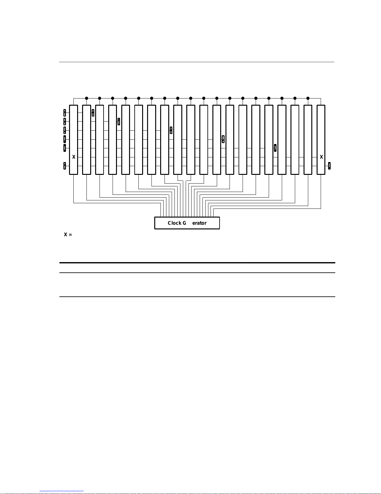
Figure 2–4. GTLP EVM Backplane Block Diagram
Backplane Overview
Slot 1
Slot 2
Slot 3
Slot 4
Slot 5
Slot 6
Slot 7
Slot 8
Slot 9
X X
Clock Generator
X = Termination Card on Back of Connector
Slot 10
Slot 11
Slot 12
Slot 13
Slot 14
Slot 15
Slot 16
Slot 17
Slot 18
Slot 19
Slot 20
Table 2–1. GTLP EVM Group Assignment
Group 6 Group 5 Group 4 Group 3 Group 2 Group 1
2 slots 4 slots 8 slots 12 slots 16 slots 20 slots
P1-1 to P1-2 P1-1 to P1-4 P1-1 to P1-8 P1-1 to P1-12 P1-1 to P1-16 P1-1 to P1-20
A single GTLP clock line that runs from P1-1 to P1-20 is used in the
source-synchronous transfer mode.
The GTLP clock and the data lines from groups 2 through 6 have fixed,
on-board, 25-Ω termination resistors. Group 1 data lines terminate on plug-in
cards on the back of the backplane board at P1-1B and P1-20B. This provides
a way to vary the termination resistance or demonstrate other termination
techniques.
The design also uses a system clock that is generated on the clock-driver
board plugged into P3. This system clock is distributed to all 20 slots
simultaneously and is used as the system master timing in the system-clock
mode. Using a separate card for clock generation and distribution is not an
industry standard, but it provides flexibility in using this demonstration board.
2-5 GTLP EVM Board Typical Test and Setup Configuration
Page 22
Backplane Board
A logic selection line (MODESEL) connects P1-1 through P1-20. The driver
card uses this line to select between source-synchronous and system-clock
operation. The demonstration board is an eight-layer board with separate V
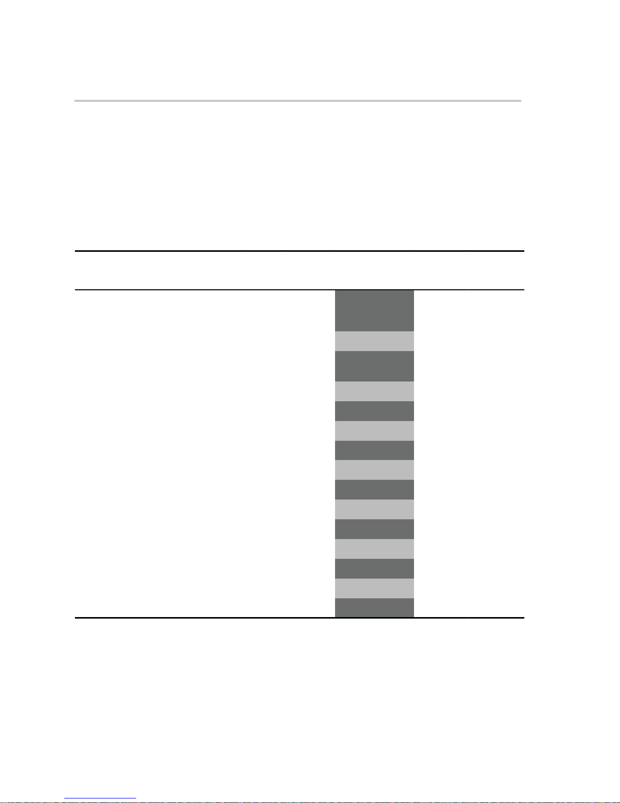
and ground planes. The backplane board stackup is shown in Table 2–2.
Embedded microstrip nominal line width is 0.006 in., dielectric material is
Nelco N4000-13 with a dielectric constant (50% resin contents) of
3.80 @ 100 MHz.
Table 2–2. GTLP EVM Backplane Eight-Layer Stackup
CC
Trace Name Use Layer
Top Regulator power/
bypass capacitor/
termination
Internal signal 2 Clock distribution/
signal
Ground plane Ground plane 3 1
Internal signal 3 Data signal 4 1
Internal signal 4 Data signal 5 1
V
CC
V
CC
1 0.5
2 1
6 1
Copper
Weight
(oz)
Physical
Representation
Dielectric
Height
(in.)
0.004 B stage
0.004 Core
0.004 B stage
0.058 Core
0.004 B stage
0.004 Core
Dielectric
Name
Internal signal 5 Data signal 7 1
Bottom Termination 8 0.5
2-6
0.004 B stage
Page 23

Backplane Board
Targeted, nominal, unloaded line impedance was 50 Ω, but, based on
post-manufacturing testing, was not consistent. Results for Group 1, bits 1
through 8 are shown in T able 2–3. The backplane natural trace impedance (Z
is calculated and is a best estimate. The backplane trace impedance with only
the connector pins attached (i.e., all cards removed) (Z
′) and the backplane
o
trace impedance in a fully loaded backplane (i.e., 20 cards inserted) (Z
measured.
Table 2–3. GTLP EVM Group 1, Bits 1 Through 8 Trace Impedance
Group 1 Trace D1 D2 D3 D4 D5 D6 D7 D8
Natural Trace Impedance
Zo (Ω) 91 47.5 47 47 48 47.5 83 47.5
tpd (ps/in.) 165 140 138 139 141 148 147 142
C
(pF/in.) 1.81 2.95 2.94 2.96 2.94 3.12 1.77 2.99
o
Trace Impedance With Only Connectors
Zo′ (Ω) 62.7 37.5 37 36.3 37.1 37.9 58.5 36.8
′′) are
o
)
o
tpd′ (ps/in.) 240 177 175 180 183 185 208 183
Trace Impedance Under Full Load
Zo′′ (Ω) 26.6 17.7 17.9 17.5 17.9 18 24.8 17.7
tpd′′ (ps/in.) 564 377 362 373 377 390 493 382
Note the difference in fully loaded trace impedance between trace bit 1 and
bit 7 (D1 and D7) and the other traces. Using the lower natural trace
impedance offers the advantage of a smaller t
and shorter flight time, but at
pd
the expense of terminating with a lower-value termination resistor and the
subsequent increase in power consumption. TI offers both medium-drive
(50 mA) and high-drive (100 mA) GTLP devices that allow designers to match
the device with backplane loading. The termination resistor (R
) should
TT
match the fully loaded trace impedance (i.e., Zo′′) of the backplane for optimal
signal integrity.
2-7 GTLP EVM Board Typical Test and Setup Configuration
Page 24
Connectors
2.4 Connectors
An AMP Z-P ACK 2-mm, 110-pin, hard-metric (HM) male connector is used
in slots 1 through 20 (see Figure 2–5) .
Figure 2–5. AMP Z-PACK 2-mm, 110-Pin, Hard-Metric (HM) Male Connector
Five pins are used on the backplane, with three different lengths on the
backplane daughter-card side. Pins A, B, and C are used for data/VCC,
BIAS V
, and GND, respectively. C-length pins are in the center, and
CC
A-length pins are in two rows on either side. The daughter-card connectors
P1-1 through P1-20 use these three levels of pin height for power sequencing.
The ground pins make contact first, followed by a pin for BIAS V
other connections are made. There is only one B-length pin because BIAS V
, then all
CC
CC
can be distributed to all four GTLP devices on the board. The pin lengths of
pins K and T are identical to those of pins A and C on the card side, but they
protrude through the backplane board, providing connection to the termination
cards that are on the reverse side.
Initial testing revealed that this pin configuration was unacceptable for actual
operation because the BIAS V
circuitry was disabled before all I/O pins were
CC
connected. Any tilt on the card caused VCC to be connected first. Some slots
in selected EVMs have been modified, so that BIAS V
and GND are
CC
C length, data signal is B length, and VCC is A length, to allow proper operation
of the BIAS V
precharge circuitry.
CC
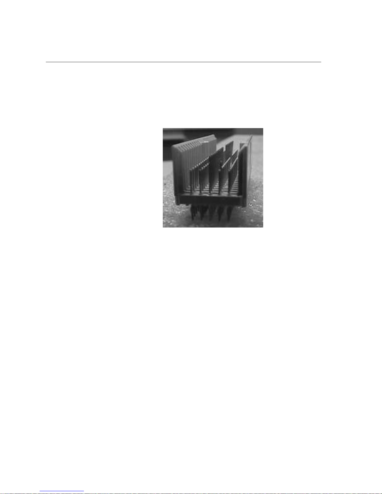
Various AMP pin lengths, including pins A, B, C, K, and T, are shown in
Figure 2–6, and the single-line-model data sheet is shown in Figure 2–7.
2-8
Page 25
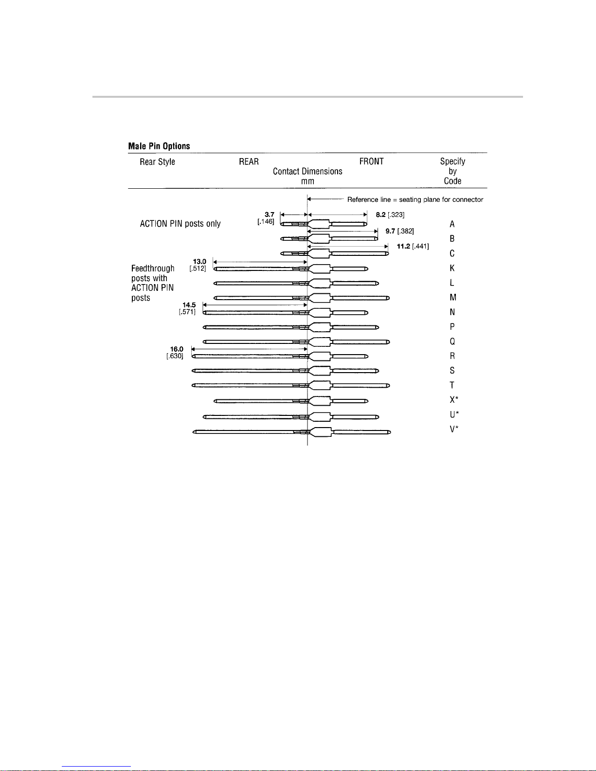
Figure 2–6. AMP Pin Lengths
Connectors
* X, U, V are used only for cross-connect applications. Not all versions are tooled.
2-9 GTLP EVM Board Typical Test and Setup Configuration
Page 26

Connectors
Figure 2–7. AMP Single-Line-Model Data Sheet
2-10
Page 27
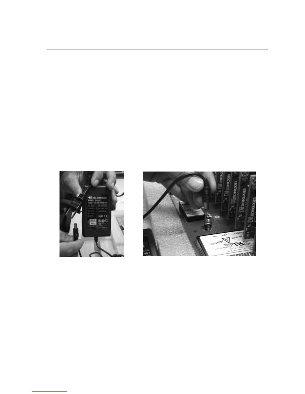
2.5 Power Supply
The power supply (see Figure 2–8) is a universal power supply that accepts
100 V to 240 V , 50/60-Hz ac and uses any wall plug that connects to the IEC
320 two-connector universal socket with the US/Canada Edison plug. An
alternate supply cord with a different wall plug must be procured locally, if
required.
The power-supply output is 24-Vdc at 2.1 A, which is fed to the backplane
board using the 5.5-mm plug to J5 (see Figure 2–8), and connects through a
2.5-A slow-blow fuse (F1). Power should not be applied to the backplane board
until the cards have been inserted during the initial setup because the clock
card is not hot insertable. The termination, daughter cards, and clock crystals
are live insertable and can be inserted and removed to change position/values
during testing without disconnecting the power supply.
Figure 2–8. Power Supply (Left) and Backplane Connection (Right)
Power Supply
The 24-Vdc is reduced to 5 V, 1 A by the Lambda PM10-24S05 switching
regulator (Figure 2–8 background) and to 3.3 V, 7.5 A by the Lambda
PM30-24503 switching regulator (Figure 2–8 foreground) for V
and the linear regulator. The 3.3 V is supplied to all connectors through a 5-A
fuse (F2). The 5 V also is applied to all connectors. Originally , F2 was specified
as a 3.5-A fuse, but, at 100-MHz operation, current exceeds this value, so 5-A
fuses are necessary.
, BIAS VCC,
CC
2-11 GTLP EVM Board Typical Test and Setup Configuration
Page 28
Power Supply
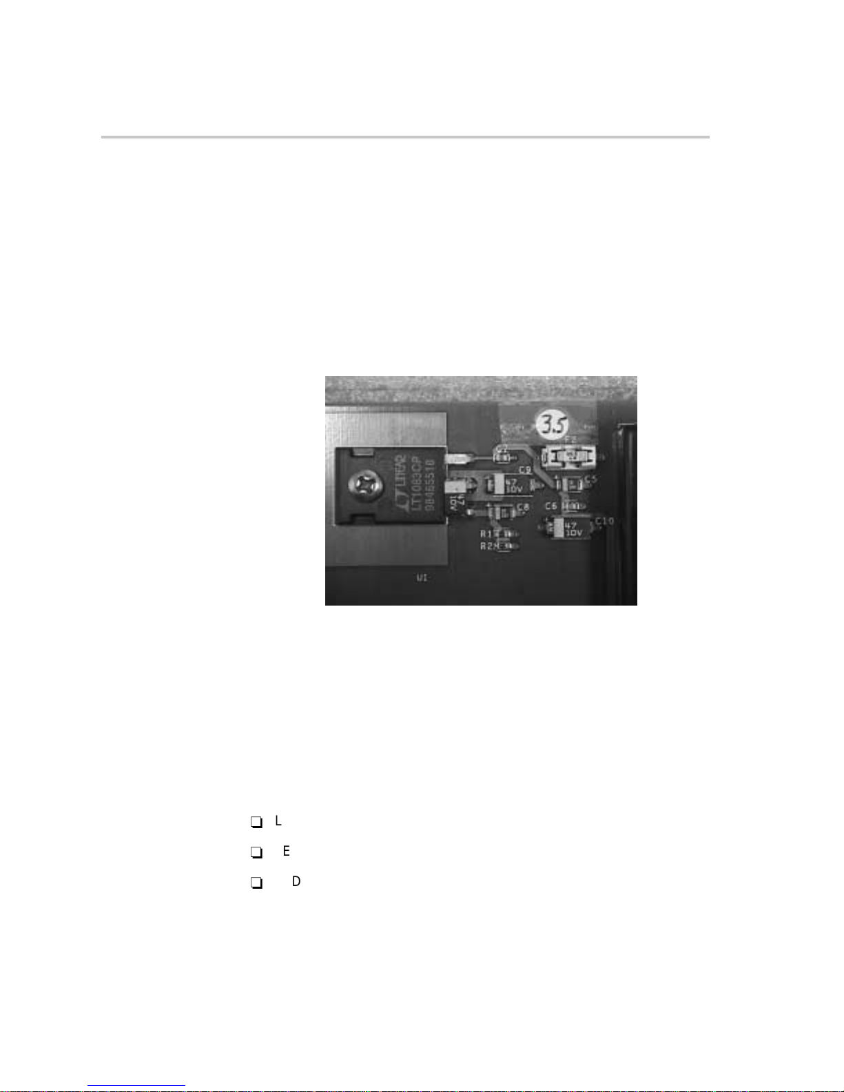
The 3.3 V is further reduced to 1.5 V , 7.5 A by the LT1083CP linear regulator
(see Figure 2–9) for the termination voltage (VTT). VTT is set by the
combination of R1 and R2 and can be varied in the factory between 0.8 V to
1.8 V, but is set at 1.0 V for field use at GTLP levels. The 5-V power supply is
required for driver cards that use both 5-V and 3.3-V V
SN74GTLPH16612. There is an option to change the 5-V power supply to
2.5 V for future devices at that voltage node. This is accomplished by removing
JP1 (near the dc converter) and installing an LM317M regulator (U2), R5, and
R6. The two resistors set the output voltage of the regulator.
Figure 2–9. 1.5-V VTT Linear Regulator
, such as the
CC
Unitrode offers two devices (UC382 and UC385) that can be used in place of
the LT1083CP. They offer low dropout at a given current (500-mV dropout
maximum at 5 A), the ability to handle transients with tight regulation,
high-current capability, fast transient response, separate bias and V
pins,
in
and 5-pin TO220 and TO263 packages with Kelvin sensing. UC382 provides
3-A capacity and UC385 provides 5-A capacity with fixed (1.5 V, 2.1 V, or
2.5 V) or adjustable-output-voltage capability.
Power-supply operation indication is provided by three LEDs (see
Figure 2–10) on the upper edge of the backplane opposite slot 16:
-
LED 1 – 24-V green LED shows there is power coming to the board.
-
LED 2 – 5-V green LED shows the 5-V power supply is operational.
-
LED 3 – 3.3-V red LED shows the 3.3-V power supply is supplying power
to the devices, BIAS VCC, and linear regulator.
2-12
Page 29

Figure 2–10. Power-Supply LED Indicators
Power Supply
2-13 GTLP EVM Board Typical Test and Setup Configuration
Page 30

Clock Crystals
2.6 Clock Crystals
Clock frequency is controlled by the clock-driver card and is limited by
clock-control components to 100 MHz. The GTLP receiver device is used in
a latched mode of operation, so GTLP data frequency is equal to one-half the
clock frequency . Clock crystals and spares, in frequencies of 66 MHz, 75 MHz,
87 MHz, and 100 MHz, are included with the kit. One crystal can be installed
on each clock card, with the others stored in the clock-crystal tube (see
Figure 2–11).
Figure 2–11.Clock Crystal on Card (Left) and Stored in Tube (Right)
If you plan to store the clock-driver card with the crystal installed, insert the
crystal far enough so that the leads barely protrude on the opposite side (see
Figure 2–12). This prevents bending the leads if they catch on the foam when
the card is placed in the case.
Figure 2–12. Clock Crystal With Leads in Position for Storage
2-14
Page 31

2.7 Termination Cards
Because proper backplane termination has a large effect on signal integrity
and is investigated easily, Group 1 has removable termination cards on the
back of the backplane (see Figure 2–13). The termination cards are identical,
except for the resistor values that are 25 Ω, 33 Ω, 38 Ω, or 50 Ω. One bypass
capacitor is mounted with every other termination resistor to limit voltage
fluctuations. The termination cards provide a method of varying the
termination resistance to only Group 1 data lines. These termination resistors
connect to the V
Figure 2–13. Termination Card Location (Left) and Close-Up View (Right)
supply (1.5 V because GTLP levels are used).
TT
Match Dots
Termination Cards
Connector Key.
Can be reversed, so
ensure that dots are
on the same side.
The termination cards have a four-layer stackup. The stackup is signal layer,
VCC plane, ground plane, and signal layer (see Table 2–4).
2-15 GTLP EVM Board Typical Test and Setup Configuration
Page 32

Termination Cards
Table 2–4. Termination-Card Stackup
Trace Name Use Layer
Top Data signal 1 0.5
V
plane VCC plane 2 1
CC
Ground plane Ground plane 3 1
Bottom
Data signal 4 0.5
Groups 2 through 6 have 25-Ω fixed termination resistors due to space
limitations, and have one bypass capacitor for every four termination resistors.
The 25-Ω termination is optimized for estimated 25-Ω loaded-line impedance.
The termination cards can remain installed on the backplane board or be
removed during storage and transit. Both termination cards can be stored in
the same slot in the tray (see Figure 2–14) or stored separately. If stored
together, the resistor/capacitor sides must face each other.
Figure 2–14. Termination-Card Storage
Copper
Weight (oz)
Physical
Representation
Dielectric
Height (in.)
0.004 B stage
0.004 Core
0.004 B stage
Dielectric
Name
2-16
Page 33

2.8 Bottom Compartment
The portable oscilloscope and backplane daughter cards are stored under the
top tray of the GTLP EVM case (see Figure 2–15).
Figure 2–15. Oscilloscope and Backplane Daughter-Card Storage Area
Clock
Cards
Bottom Compartment
Monitored
Receiver
Cards
Oscilloscope
Storage
Driver
Cards
Unmonitored
Receiver
Cards
Empty
Slots
There are 2 clock cards, 19 unmonitored receiver cards, 3 monitored receiver
cards, and 2 driver cards in every GTLP EVM kit. Store the cards as shown
in Figure 2–15, with the 2 clock cards (top left) followed by 10 unmonitored
receiver cards, 3 monitored receiver cards (middle left) followed by
9 unmonitored receiver cards, 2 driver cards (bottom left) followed by
10 empty slots.
2-17 GTLP EVM Board Typical Test and Setup Configuration
Page 34
Measurement Equipment
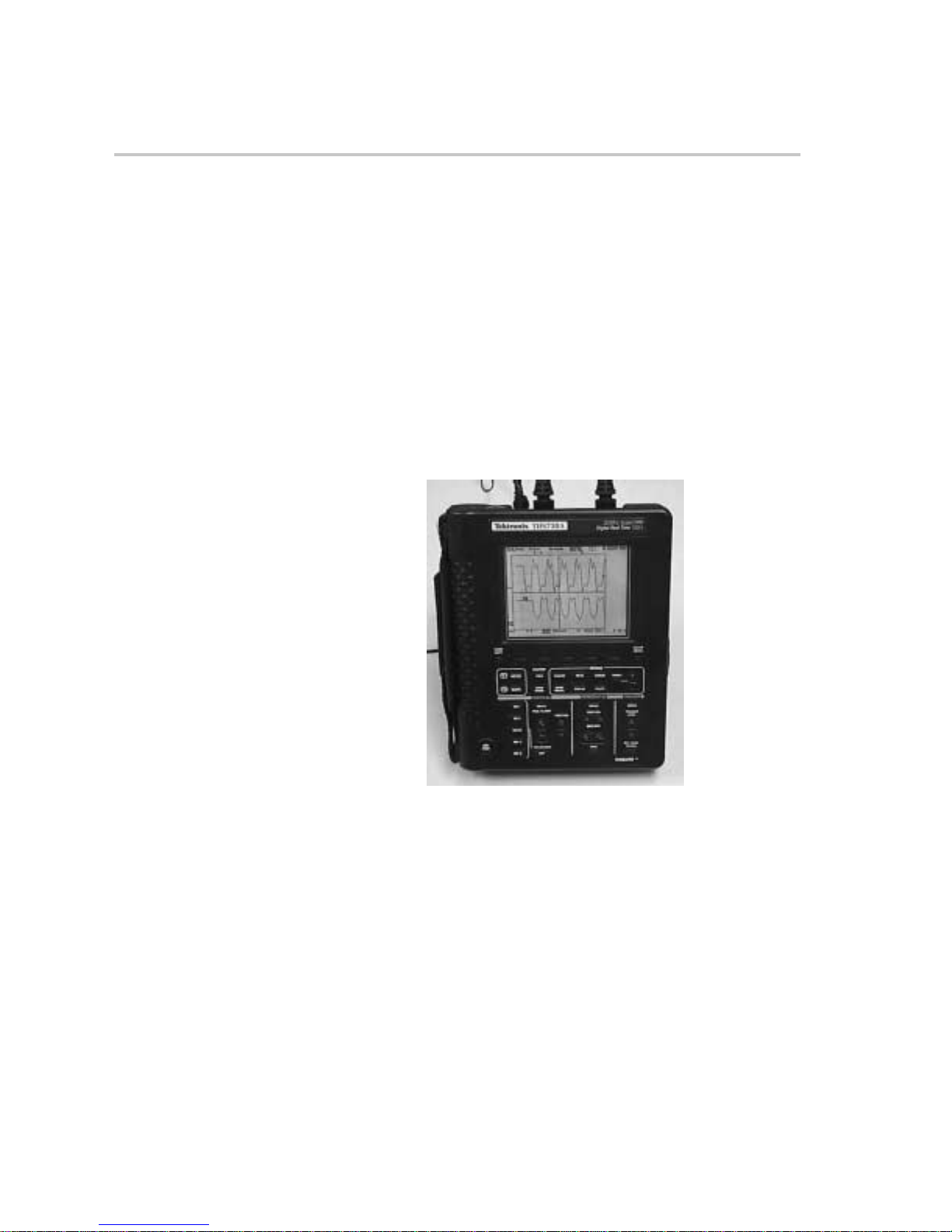
2.9 Measurement Equipment
The T ektronix THS730A Oscilloscope/DMM (O-Scope) (see Figure 2–16) can
be stored in the bottom of the case (see Figure 2–15). It is easy to operate and
is portable. The O-Scope can monitor two channels simultaneously . Store the
O-Scope face down to prevent damage to the buttons during transit. The
probes can be stored on top of the O-Scope, as shown, or alongside,
depending on the amount of space in either location. The O-Scope is not
included with the loaned EVM kits. Chapter 3, Oscilloscope Operation,
discusses O-Scope setup and operation and is included to provide assistance
to TI product marketing engineers and technical sales representatives when
demonstrating the GTLP EVM to customers in the field.
Figure 2–16. Tektronix THS730A O-Scope
2-18
Page 35

2.10 Clock Cards
Two clock cards (see Figure 2–17) are included with the EVM, one primary and
one spare. The clock cards generate the clock signal that is sent to every slot
via mitered lines, so that the clock arrives at exactly the same time at each
card. The clock card uses a plug-in half-can oscillator for a reference to two
CDC2586 phase-locked-loop clock drivers. These two drivers provide the
20 system clocks used on the backplane. The CDC2586 supports a maximum
frequency of 100 MHz. The clock card has one subminiature B connector
(SMB) as specified by MIL-C-39012 coaxial connector specification test point
to monitor the oscillator output.
Figure 2–17. GTLP EVM Clock Card
Clock Cards
The clock-card board is a four-layer printed circuit board (PCB). The stackup
is signal layer, VCC plane, ground plane, and signal layer (see Table 2–5).
2-19 GTLP EVM Board Typical Test and Setup Configuration
Page 36
Clock Cards
Table 2–5. Clock-Card Stackup
Copper
Trace Name Use Layer
Top Data signal 1 0.5
V
plane VCC plane 2 1
CC
Ground plane Ground plane 3 1
Bottom
Data signal 4 0.5
Weight (oz)
Physical
Representation
Dielectric
Height (in.)
0.004 B stage
0.004 Core
0.004 B stage
Dielectric
Name
2-20
Page 37

2.11 Driver Cards
Separate driver and receiver daughter cards were manufactured for use on the
backplane because, even though the bidirectional SN74GTLPH1655 device
is used, each type of card is hardwired to operate in a certain direction. The
driver card generates a data pattern from the system clock and drives the
GTLP lines on the backplane. The GTLP devices are hardwired for clocked
storage in the A-to-B direction. Data is transmitted on the rising edge of the
system clock. The driver card is a six-layer PCB with two signal layers, a
plane, a ground plane, then two signal layers. Stackup is shown in
V
CC
Table 2–6.
Table 2–6. Driver-Card Stackup
Driver Cards
Copper
Trace Name Use Layer
Top Data signal 1 0.5
Internal signal 2 Data signal 2 1
V
plane VCC plane 3 1
CC
Ground plane Ground plane 4 1
Internal signal 3 Data signal 5 1
Bottom
Data signal 6 1
Weight (oz)
Physical
Representation
Dielectric
Height (in.)
0.004 B stage
0.004 Core
0.004 B stage
0.004 Core
0.004 B stage
Dielectric
Name
2-21 GTLP EVM Board Typical Test and Setup Configuration
Page 38

Driver Cards
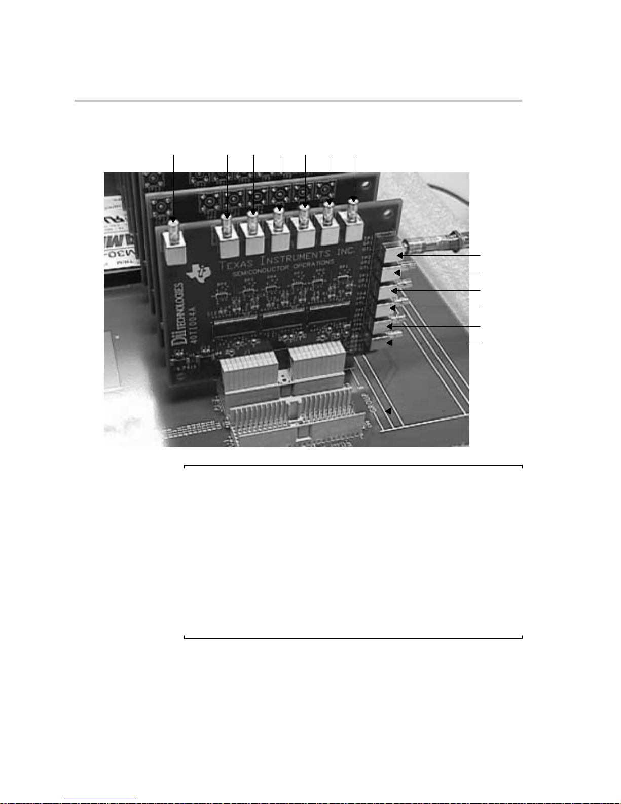
The driver daughter card (see Figure 2–18) has SMB monitor points for
selected LVTTL and GTLP signals, in addition to jumpers for Group 1, bit 1
switching (JB1), system or SN74GTLP1394 source-synchronous clock
selection (JB2), and selection of the SN74GTLPH1655 slow or fast edge rate
(JB3). The monitor points along the top edge are the latch clock and the master
data pattern sent to all SN74GTLPH1655 L VTTL A-port inputs. There are no
LVTTL group-bit monitor points because the card always is driven. Monitor
points along the right edge are GTLP Group 1, 2, 3, 4, 5, and 6. The following
signals are monitored:
-
TP1 GTLP level Group 1, bit 1
-
TP2 GTLP level Group 2, bit 1
-
TP3 GTLP level Group 3, bit 1
-
TP4 GTLP level Group 4, bit 1
-
TP5 GTLP level Group 5, bit 1
-
TP6 GTLP level Group 6, bit 1
-
TP7 LVTTL level Group 1, bit 1, and master data pattern
-
TP8 LVTTL level GTLP latch clock
Figure 2–18. GTLP EVM Driver Daughter Card
TP7
JB1
TP8
GTLPH1655
GTLP1394
JB2
2-22
JB2
TP1
TP2
TP3
TP4
TP5
TP6
Page 39

Driver Cards
r
2.11.1 Single-Bit Selection
JB1 three-position jumper is used to set Group 1, bit 1 to pass the normal data
pattern, set the signal low, or set the signal high (see Figure 2–19). The JB1
jumper is stored on the lowest pin (see Figure 2–19) when set high, to prevent
losing it. The following options are available:
-
JB1 1-2 shorted Group 1, bit 1 normal data pattern
-
JB1 2-3 shorted Group 1, bit 1 held low
-
JB1 open Group 1, bit 1 held high
Figure 2–19. Bit Selection for Normal Data Pattern (Left), Signal Held Low (Center), or
Signal Held High (Right)
JB1 Jumpe
2-23 GTLP EVM Board Typical Test and Setup Configuration
Page 40

Driver Cards
2.11.2 Edge-Rate Control
The device used as the backplane driver, SN74GTLPH1655, has a feature by
which the backplane slew rate is adjustable via an external edge-rate-control
(ERC) pin held at 3.3 V (slow) or GND (fast). The ERC is set by the JB3 jumper
located below the bit-selection jumper and has two positions: not connected
is slow, and shorted is fast (see Figure 2–20). The following ERC options are
available:
-
JB3 open Slow edge rate
-
JB3 shorted Fast edge rate
Figure 2–20. ERC Bit-Selection Jumper Set for Slow (Left) or Fast (Right) Rate
JB3 Jumper
2-24
Page 41

2.11.3 Source-Synchronous Clock/System-Clock Selection
Backplanes usually have a system-wide synchronous clock. A system clock
provides an absolute reference time signal from the clock card to every
daughter card at exactly the same time. Source-synchronous clock operation
is different because it allows the absolute system clock to be sent by the
backplane driver along with the data. In the EVM, this is implemented with the
SN74GTLP1394 transceiver on all daughter cards. This transceiver acts as
the driver on the driver cards and as the receiver on the receiver cards. The
SN74GTLP1394 has ERC that is set to the fast edge rate in conjunction with
the JB3 selection.
Source-synchronous clock operation provides a relative clock to all receiver
cards, which removes the flight-time delay restrictions required when an
absolute system clock is used. The flight-time delay depends primarily on bus
length and bus loading.
The driver card uses JB2 to select the transfer mode of operation and to drive
the MODESEL line. Source-synchronous clock operation is selected when the
JB2 jumper shorts the pins, and system-clock operation is selected when the
pins are open (see Figure 2–21). When JB2 is shorted, the SN74GTLP1394
drives the GTLP clock line with a phased system clock. When JB2 is open,
there is no activity on the GTLP clock line. The following options are available:
Driver Cards
-
JB2 shorted Source-synchronous clock transfer
-
JB2 open System-clock transfer
Figure 2–21. JB2 Set to Source-Synchronous Clock (Left) or System-Clock (Right)
Operation
2-25 GTLP EVM Board Typical Test and Setup Configuration
Page 42

Receiver Cards
2.12 Receiver Cards
Receiver cards place a load on the backplane and provide a point to monitor
the signals. There are two types of receiver cards: one that has built-in monitor
points, and one with no monitor points. Either type can be placed in any slot
in the backplane, typically with the monitored receiver card placed in the slots
under observation. There is a monitor point for only one bit per group. Only a
few receiver cards have monitor points because the capacitance added by the
monitor point affects backplane signal integrity . Minimal use of the monitored
receiver card is encouraged because of the increased loading this card
causes.
Receiver cards have GTLP devices hardwired for clocked storage in the
B-to-A direction. Data is latched on the rising edge of the GTLP latch clock. The
latch clock comes from the system clock when the MODESEL line is high, and
from the GTLP clock when the MODESEL line is low. The receiver card is a
six-layer PCB with two signal layers, a V
signal layers. The GTLP data and clock stub lines are approximately 1 in. in
length. Stackup is shown in Table 2–7.
Table 2–7. Receiver-Card Stackup
plane, a ground plane, then two
CC
Copper
Trace Name Use Layer
Top Data signal 1 0.5
Internal signal 2 Data signal 2 1
V
plane VCC plane 3 1
CC
Ground plane Ground plane 4 1
Internal signal 3 Data signal 5 1
Bottom
Data signal 6 1
Weight (oz)
Physical
Representation
Dielectric
Height (in.)
0.004 B stage
0.004 Core
0.004 B stage
0.004 Core
0.004 B stage
Dielectric
Name
2-26
Page 43

Receiver Cards
Figure 2–22 shows a monitored receiver card. Monitor points on the right side
are for GTLP Groups 1, 2, 3, 4, 5, and 6. Monitor points on the top are for L VTTL
latch clock, Groups 6, 5, 4, 3, 2, and 1. The L VTTL latch-clock source is either
the system clock or source-synchronous clock. The source-synchronous
clock is the system clock sent via the SN74GTLP1394 driver card along the
1-bit clock trace on the backplane to the SN74GTLP1394 receiver card that
converts it back to LVTTL logic levels.
The monitored receiver card has SMB jacks to monitor selected signals:
-
TP1 GTLP level Group 1, bit 1
-
TP2 GTLP level Group 2, bit 1
-
TP3 GTLP level Group 3, bit 1
-
TP4 GTLP level Group 4, bit 1
-
TP5 GTLP level Group 5, bit 1
-
TP6 GTLP level Group 6, bit 1
-
TP7 LVTTL level Group 1, bit 1
-
TP8 LVTTL level Group 2, bit 1
-
TP9 LVTTL level Group 3, bit 1
-
TP10 LVTTL level Group 4, bit 1
-
TP11 LVTTL level Group 5, bit 1
-
TP12 LVTTL level Group 6, bit 1
-
TP13 LVTTL level GTLP latch clock
2-27 GTLP EVM Board Typical Test and Setup Configuration
Page 44
Receiver Cards
Figure 2–22. GTLP EVM Monitored Receiver Card
TP13 TP12 TP11 TP10 TP9 TP8 TP7
TP1
TP2
TP3
TP4
TP5
TP6
Note:
SN74GTL1655 devices were used on the receiver cards. The
SN74GTLPH1655 was in development and initial preproduction samples
were used for the driver cards, but insufficient quantities were available for
the receiver cards. The SN74GTL1655 and SN74GTLPH1655 are identical,
except for the B-port output edge rate (slew) and B-port C
. Because the
io
GTLP signals only are received by the receiver cards, it is essentially
immaterial which devices are used on the receiver cards, because both have
the same differential input (except for the difference in B-port C
, which is
io
6 pF typical and 8 pF maximum for the SN74GTL1655, and 8.5 pF typical and
10.5 pF maximum for the SN74GTLPH1655). GTLP devices have a larger
B-port C
, because a larger transistor and ESD cell is required by the newer
io
CMOS process.
2-28
Page 45
Backplane Setup
2.13 Backplane Setup
2.13.1 Insertion of Clock Cards
The clock-card connectors (see Figure 2–23) use AMP 55-pin, 2-mm, HM
connectors and are identical to the backplane termination-card connectors.
They can be mated improperly because they are keyed only on one side,
whereas the backplane connectors are keyed in the center and do not allow
improper insertion.
The clock card should be inserted or removed from the backplane
only after power has been disconnected, to prevent damage to the
CDC components.
Figure 2–23. AMP Z-PACK, 2-mm, 55-Pin, HM Male (Left) and Female (Right)
Clock-Card Connectors
Connector Key
Figure 2–24 shows the mating sequence. When mated, the connectors should
be firm with no lines showing. Some rocking action might be required to seat
or remove the connectors, but should be minimal to prevent bending the pins.
Connector Key
2-29 GTLP EVM Board Typical Test and Setup Configuration
Page 46

Backplane Setup
Figure 2–24. Connector Premate (Left), Mating (Center), and Mated (Right)
Key
Figure 2–25 (left) shows the clock card properly inserted, with the CDC
components and the clock crystal facing away from the backplane connectors
and daughter cards. Y ellow dots are located on the connector and the card to
help ensure proper orientation. Figure 2–25 (right) shows the card
improperly inserted.
Figure 2–25. Clock Card Properly (Left) and Improperly (Right) Inserted
Match
Dots
2-30
Page 47

2.13.2 Insertion of Clock Crystals
Clock crystals are live insertable, unlike the clock card, which is not live
insertable. Clock crystals are inserted easily on the clock card by pulling off
one crystal and inserting the new crystal (see Figure 2–26). The leads can be
bent gently to ease insertion. The clock crystal need not be inserted fully flush
with the card for proper operation. In fact, this condition is preferred if the clock
card is stored with the crystal inserted, otherwise, the foam liner can bend the
exposed leads.
Figure 2–26. Clock Crystal Removal (Left) and Insertion (Right)
Backplane Setup
2-31 GTLP EVM Board Typical Test and Setup Configuration
Page 48

Backplane Setup
2.13.3 Insertion of Termination Cards
Termination-card, AMP Z-PACK, 2-mm, 55-pin, HM male and female
connectors are identical to the clock-card connectors, and are inserted directly
onto the K and T pins used for slots 1 and 20, V
termination card connectors are keyed on the top (see Figure 2–27), they can
be inserted backward because they are keyed on only one side.
Figure 2–27. Termination-Card Keying
Be sure that the red dot on the male connector and the card are facing each
other, to prevent improper operation. Both termination-card components face
the same direction, toward slot 20, so the key to proper operation is to inspect
for the keying and line up the red dots (see Figure 2–28). If the backplane is
not working, the proper orientation of the termination cards should be the first
thing you check. The cards can be rocked slightly side to side to seat and
remove them, but avoid bending the pins.
, and data bits. Although the
CC
Keying
Figure 2–28. Slot 1 (Left) and Slot 20 (Right) Termination Cards on the Backplane
2-32
Page 49

2.13.4 Insertion of Driver and Receiver Cards
The driver and receiver cards are live insertable and are easy to insert and
remove, although some slight side-to-side rocking action might be required.
The cards can be inserted into any slot in any order, but only one driver card
should be used at any one time. There is no bus contention damage if multiple
driver cards are in operation at the same time, this is one key benefit from using
the GTLP open-drain technology. Figure 2–29 shows the connector keying
that allows the cards to be placed on the connector in only one direction. When
inserted properly, the component side of the card faces slot 1.
Figure 2–29. Driver and Receiver Connector Keying
Backplane Setup
Keying
Figure 2–30 shows the keying in more detail. The upper key is wider than the
lower key, preventing improper insertion.
2-33 GTLP EVM Board Typical Test and Setup Configuration
Page 50

Backplane Setup
Figure 2–30. Close-up View of Connector Keying
Wide Key
Narrow Key
The card should be placed squarely on the connector and pressed down (see
Figure 2–31), with very little side-to-side motion. The components are facing
left towards slot 1, the power supplies are on the top/right, and the Group 1–6
markings are on the bottom/left. The card in Figure 2–31 is being inserted into
slot 20.
Figure 2–31. Proper Connector Mating Sequence (Left to Right)
Figure 2–32 shows the connectors properly mated.
2-34
Page 51

Figure 2–32. Connectors Properly Mated
Backplane Setup
2-35 GTLP EVM Board Typical Test and Setup Configuration
Page 52

Chapter 3
Oscilloscope Operation
Topic Page
3.1 Oscilloscope Setup 3-2. . . . . . . . . . . . . . . . . . . . . . . . . . . . . . . . . . . . . . . . . . .
3.2 Measurements 3-3. . . . . . . . . . . . . . . . . . . . . . . . . . . . . . . . . . . . . . . . . . . . . . . .
3-1
Page 53
Oscilloscope Setup
3.1 Oscilloscope Setup
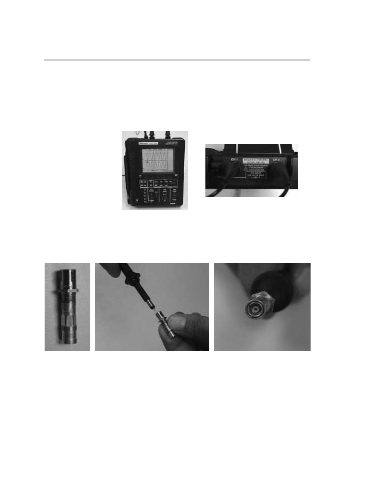
The recommended oscilloscope (O-Scope) for the GTLP EVM is the T ektronix
THS730A (see Figure 3–1). It allows only two-channel operation, which should
be sufficient for most investigations done with the demonstration backplane.
Figure 3–1. Tektronix O-Scope Front (Left) and Top (Right)
SMB adapters (see Figure 3–2) are needed to properly mate T ektronix probes
with the test points. These adapters are custom built for the T ektronix O-Scope
probes and are not normally included in the GTLP EVM.
Figure 3–2. O-Scope Probe Monitor-Point Adapters
3-2
Page 54

3.2 Measurements
The first step in taking measurements is to plug one probe into channel 1
(CH 1) of the O-Scope and connect the opposite end to the desired monitor
point. Plug the other probe into channel 2 (CH 2) of the O-Scope and connect
the opposite end to the desired monitor point (see Figures 3–1 and 3–3).
Chapter 4, Waveform Measurement and Interpretation, discusses which
monitor points should be used and why.
Figure 3–3. Simple Test-Measurement Connection
Measurements
Press the ON/STBY button on the O-Scope (see Figure 3–4), and press the
CH 1 or CH 2 button.
Figure 3–4. Turn On O-Scope (Left) and Select Channel (Right)
3-3Oscilloscope Operation
Page 55

Measurements
Waveforms similar to those in Figure 3–5, depending on how the O-Scope
presets were set, are displayed. In Figure 3–5, CH 2 is selected.
Figure 3–5. O-Scope Display
3-4
Page 56

To adjust the timing (x or horizontal axis), press the appropriate side of the
SEC/DIV button (see Figure 3–6). An example of the results is shown for
50 ns/division and 100 ns/division. Timing is the same for both channels and
is independent of channel selection.
Figure 3–6. Timing Adjustment
To adjust the voltage (y or vertical axis), press the top or bottom of the
VOLTS/DIV button (see Figure 3–7). An example of the results is shown for
Ch2 at 1 V (center) and Ch2 at 2 V (right). Voltage adjustment is independent
of channels, which are selected by pressing either the CH 1 or the CH 2 button.
Measurements
Figure 3–7. Voltage Adjustment
3-5Oscilloscope Operation
Page 57

Measurements
To adjust the trigger, press the MENU button (see Figure 3–8), then press
Trigger Source to display a submenu. In the submenu, select Ch1, Ch2, or Ext
[DMM] by repeatedly pressing the same Trigger Source button. After the
appropriate trigger is selected, press the CLEAR MENU button to restore the
O-Scope to operation.
Figure 3–8. Trigger Adjustment
3-6
Page 58
Chapter 4
Waveform Measurement and Interpretation
In this chapter, five dif ferent measurement cases are discussed in detail, and
several more measurement combinations are outlined. Many other
combinations are possible.
Topic Page
4.1 Timing Relationship of Driver Card (D1) Data Pattern (Ch1) and
Driver Card (D1) Latch Clock (Ch2) 4-2. . . . . . . . . . . . . . . . . . . . . . . . . . . . .
4.2 Timing Relationship of Driver Card (D1) Data Pattern (Ch1) and
Driver Card (D1) Group 1 GTLP Data Out (Ch2) 4-3. . . . . . . . . . . . . . . . . .
4.3 Timing Relationship of Driver Card (D1) Data Pattern (Ch1) and
Receiver Card (R2) Group 1 GTLP Data In (Ch2) 4-4. . . . . . . . . . . . . . . . .
4.4 Timing Relationship of Driver Card (D1) Data Pattern (Ch1) and
Receiver Card (R2) Group 1 LVTTL Data Out (Ch2) 4-5. . . . . . . . . . . . . . .
4.5 Timing Relationship of Receiver Card (R2) Group 1 GTLP Data In
(Ch1) and Receiver Card (R20) Group 1 GTLP Data In (Ch2) 4-6. . . . . .
4.6 Monitored Waveforms 4-7. . . . . . . . . . . . . . . . . . . . . . . . . . . . . . . . . . . . . . . . .
4-1
Page 59

Timing Relationship of Driver Card (D1) Data Pattern (Ch1) and Driver Card (D1) Latch Clock (Ch2)
4.1 Timing Relationship of Driver Card (D1) Data Pattern (Ch1) and
Driver Card (D1) Latch Clock (Ch2)
Figure 4–1 shows the probe hookup and related O-Scope output for Case 1.
The LVTTL latch clock signal goes to the SN74GTLPH1655 driving device
CLK pin, and the LVTTL data signal goes to the A-port input pin, specifically
the Group 1, bit 1 data signal.
Figure 4–1. Case 1: D1 Data Pattern (Ch1) and D1 Latch Clock (Ch2)
LVTTL
Data
Input
LVTTL
Latch-Clock
Input
4-2
Page 60

Timing Relationship of Driver Card (D1) Data Pattern (Ch1) and Driver Card (D1) Group 1 GTLP Data Out (Ch2)
4.2 Timing Relationship of Driver Card (D1) Data Pattern (Ch1) and
Driver Card (D1) Group 1 GTLP Data Out (Ch2)
Figure 4–2 shows the probe hookup and O-Scope output for Case 2. The
LVTTL data goes into the SN74GTLPH1655 driving device A-port input, and
the GTLP data comes out of the B-port output. The driver-card GTLP data
output comes out after the rising edge of the clock, in addition to the CLK-to-B
propagation delay. This is why the signals look 180 degrees out of phase.
Figure 4–2. Case 2: D1 Data Pattern (Ch1) and D1 Group 1 GTLP Data Out (Ch2)
LVTTL
Data
Input
GTLP
Data
Output
4-3Waveform Measurement and Interpretation
Page 61

Timing Relationship of Driver Card (D1) Data Pattern (Ch1) and Receiver Card (R2) Group 1 GTLP Data In (Ch2)
4.3 Timing Relationship of Driver Card (D1) Data Pattern (Ch1) and
Receiver Card (R2) Group 1 GTLP Data In (Ch2)
Figure 4–3 shows the probe hookup and O-Scope output for Case 3. The
LVTTL data input goes to the SN74GTLPH1655 driving device A-port input,
and the GTLP data input goes to the SN74GTL1655 receiving device B-port
in slot 2. These waveforms look similar to those in Figure 4–2, but with slightly
more delay caused by the flight time between slots 1 and 2.
Figure 4–3. Case 3: D1 Data Pattern (Ch1) and R2 Group 1 GTLP Data In (Ch2)
LVTTL
Data
Input
GTLP
Data
Input
4-4
Page 62
Timing Relationship of Driver Card (D1) Data Pattern (Ch1) and Receiver Card (R2) Group 1 LVTTL Data Out (Ch2)
4.4 Timing Relationship of Driver Card (D1) Data Pattern (Ch1) and
Receiver Card (R2) Group 1 LVTTL Data Out (Ch2)
Figure 4–4 shows the probe hookup and O-Scope output for Case 4. The
LVTTL data input goes to the SN74GTLPH1655 driving device A-port input,
and the LVTTL data output of the SN74GTL1655 receiving device goes to
A port in slot 2. Because the GTLP EVM is clocked using the central system
clock (i.e., clock arrives at all daughter cards at the same time) the total delay
from the LVTTL data input on slot 1 to the LVTTL data output on slot 2 is the
sum of one clock cycle (20 ns), the setup time on the driver card (∼9 ns), and
the propagation delay of the GTLPH1655 CLK to A of about 3 ns. The GTLP
EVM driver card is set up to transmit sixteen bits of data and then wait eight
cycles before transmitting again. This allows the technician to determine the
total delay. In this case, assuming the waveform in Ch1 had just started, the
total delay is about 32 ns.
Figure 4–4. Case 4: D1 Data Pattern (Ch1) and R2 Group 1 LVTTL Data Out (Ch2)
Total Propagation Delay
LVTTL
Data
Input
LVTTL
Data
Output
4-5Waveform Measurement and Interpretation
Page 63
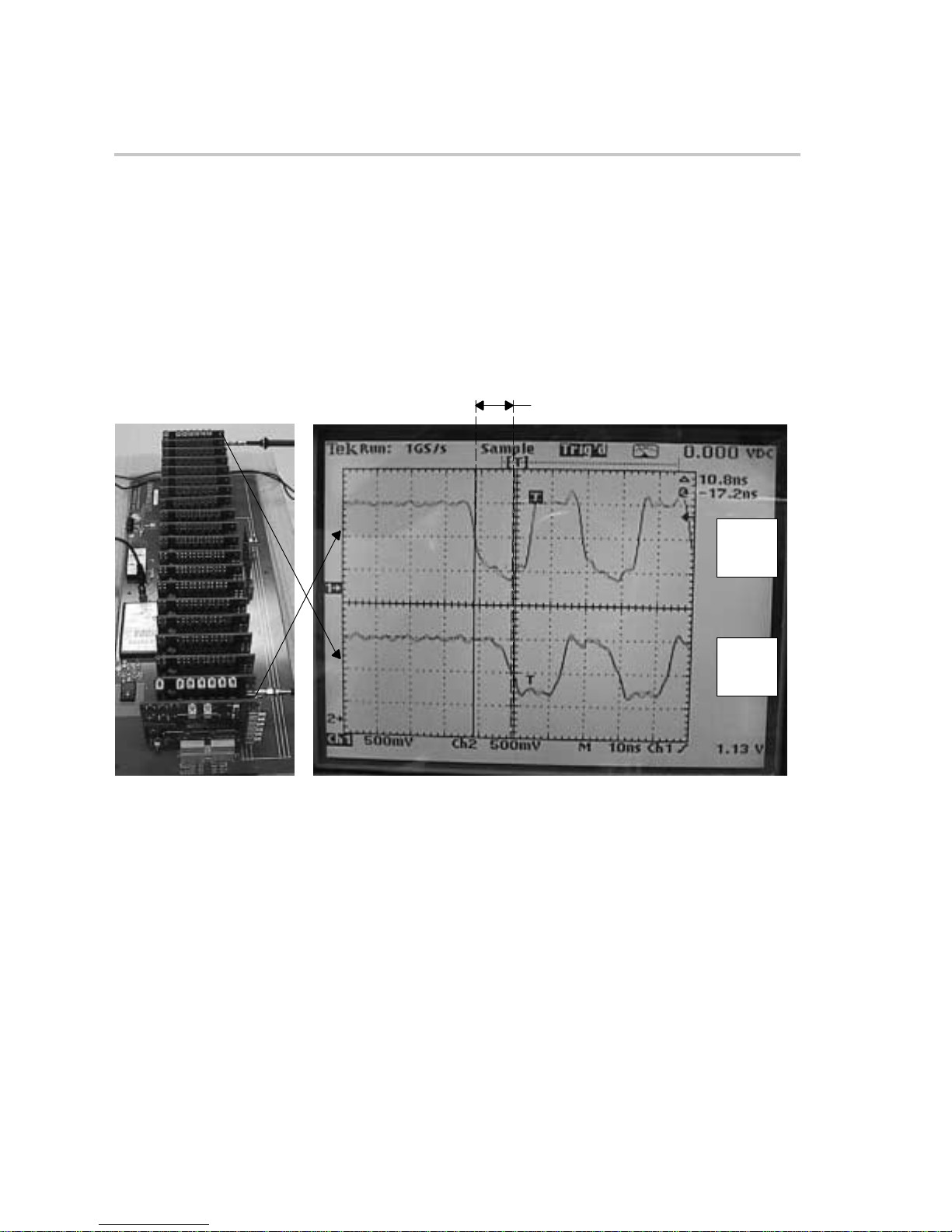
Timing Relationship of Receiver Card (R2) Group 1 GTLP Data In (Ch1)
4.5 Timing Relationship of Receiver Card (R2) Group 1 GTLP Data In (Ch1)
and Receiver Card (R20) Group 1 GTLP Data In (Ch2)
Figure 4–5 shows the probe hookup and O-Scope output for Case 5. Y ou can
see the flight-time delay between the output of the SN74GTLPH1655 driving
device B port in slot 1 and the SN74GTL1655 receiving device B port in
slot 20. Total flight time is about 9 ns.
Figure 4–5. Case 5: R2 Group 1 GTLP Data In (Ch1) and R20 Group 1 GTLP Data In
(Ch2)
Flight-Time Delay
GTLP
Data
Input
GTLP
Data
Input
4-6
Page 64

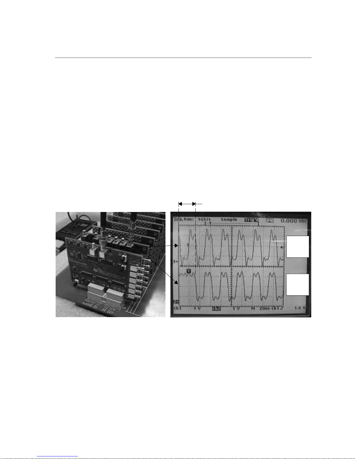
4.6 Monitored Waveforms
There are differences in waveforms between GTLP monitor test points and
measurements taken at the backplane connector pins, due to interference
from LVTTL data and clock signals not shielded adequately on the daughter
cards. This concern is only for this demonstration backplane because there is
no reason to extend the GTLP signals past the GTLP device B-port output pins
on operational daughter cards. Figures 4–6 and 4–7 show the difference
between waveforms taken directly on the backplane and those taken from the
monitor test points under fully loaded conditions at a clock frequency of
23 MHz. Waveforms shown in Figures 4–6 and 4–7 are at one-half clock
frequency, or 11.5 MHz, and are taken with various termination cards.
Figure 4–6. GTLP Backplane Waveforms at 23-MHz Clock Frequency
Monitored Waveforms
Figure 4–7. GTLP Monitor Test-Point Waveforms at 23-MHz Clock Frequency
4-7Waveform Measurement and Interpretation
Page 65

Monitored Waveforms
4-8
Page 66

Chapter 5
Troubleshooting
Topic Page
5.1 Spare Parts 5-2. . . . . . . . . . . . . . . . . . . . . . . . . . . . . . . . . . . . . . . . . . . . . . . . . . .
5.2 Replacing 5-A Fuse F2 5-3. . . . . . . . . . . . . . . . . . . . . . . . . . . . . . . . . . . . . . . .
5.3 Replacing 2.5-A Fuse F1 5-4. . . . . . . . . . . . . . . . . . . . . . . . . . . . . . . . . . . . . . .
5.4 Damage to the Daughter Cards 5-5. . . . . . . . . . . . . . . . . . . . . . . . . . . . . . . . .
5-1
Page 67

Spare Parts
5.1 Spare Parts
Each EVM is equipped with spare fuses and jumpers (see Figure 5–1).
Figure 5–1. Spare Fuses and Jumpers
5-2
Page 68

5.2 Replacing 5-A Fuse F2
Fuse F2 (see Figure 5–2) provides power from the 3.3-V switching regulator
to the 3.3-V power plane and blows if V
occur if a connector pin is bent during insertion or if measurements are taken
directly from the backplane.
F2 can be replaced easily with one of the spare fuses. Simply disconnect
power from the board, and pull out the fuse with pliers (see Figure 5–2). Push
in the new fuse, and reconnect the power supply.
Figure 5–2. Fuse F2 (Left) and Removal Procedure (Right)
Replacing 5-A Fuse F2
is shorted to GND. Shorting can
CC
5-3Troubleshooting
Page 69

Replacing 2.5-A Fuse F1
5.3 Replacing 2.5-A Fuse F1
Fuse F1 (see Figure 5–3) provides power from the power supply to the 3.3-V
and 5-V switching regulators and blows if the switching regulators fail. It is
replaced as easily as fuse F2. Disconnect the power from the board, pull out
the fuse with pliers, push in the new fuse, then reconnect the power supply.
Figure 5–3. Fuse F1
5-4
Page 70

5.4 Damage to the Daughter Cards
The daughter cards are not field repairable and must be returned to the factory
for repair.
Damage to the Daughter Cards
5-5Troubleshooting
Page 71

Damage to the Daughter Cards
5-6
Page 72

Appendix A
Appendix A
Bill of Materials, Schematics, Board Layouts,
and Suggested Specifications
Topic Page
A.1 GTLP EVM Bill of Materials A-2. . . . . . . . . . . . . . . . . . . . . . . . . . . . . . . . . . . .
A.2 Board Layouts and Schematics A-5. . . . . . . . . . . . . . . . . . . . . . . . . . . . . . . .
A-1
Page 73

GTLP EVM Bill of Materials
A.1 GTLP EVM Bill of Materials
-
Backplane
Device Type Quantity
Z-PAK 110-Pin Male Connector 20
Z-PAK 55-Pin Male Connector 1
2.5 AMP Fuseholder 1
5 AMP Fuseholder 1
Surface Mount 0.01uF Cap 3
Surface Mount 0.1uF Cap 75
Surface Mount Tantalum 10uF/10V Cap 4
Surface Mount Tantalum 1uF/35V Cap 2
Surface Mount Tantalum 47uF/10V Cap 2
Surface Mount 100 ohm Resistor 1
Surface Mount 120 ohm Resistor 1
Surface Mount 1.5K ohm Resistor 1
Surface Mount 20 ohm Resistor 1
Surface Mount 240 ohm Resistor 1
Surface Mount 25 ohm Resistor 1
Green LED 2
Red LED 1
L T1083CP Voltage Regulator 1
Powerjack 1
24V-to-5V DC-to-DC Converter 1
24V-to-3.3V DC-to-DC Converter 1
A-2
Page 74

GTLP EVM Bill of Materials
Clock Driver Card
-
Device Type Quantity
Z-PAK 55-Pin Female Connector 1
CDC2586 TQFP Clock Driver 2
Surface Mount 0.1uF Cap 10
Surface Mount 453 ohm Resistor 1
Oscillator Mount 1
SMB Coax Connector 1
-
Termination Card
Device Type Quantity
Z-PAK 55-Pin Female Connector 1
Surface Mount 0.1uF Cap 4
Surface Mount 25 ohm Resistor 8
-
Monitored Receiver Card
Device Type Quantity
Z-PAK 55-Pin Female Connector 1
10K ohm Resistor Network 6
SN74ALVC126 TVSOP Buffer 1
SN74GTLP1394 TVSOP Transceiver 1
SN74GTL1655 TSSOP UBT 3
Surface Mount 0.1uF Cap 12
Surface Mount 47pF Cap 6
Surface Mount 1K ohm Resistor 1
Surface Mount 2K ohm Resistor 1
Surface Mount 453 ohm Resistor 7
Surface Mount 51.1 ohm Resistor 13
SMB Coax Connector 13
A-3Bill of Materials, Schematics, Board Layouts, and Suggested Specifications
Page 75

GTLP EVM Bill of Materials
Monitored Driver Card
-
Device Type Quantity
Z-PAK 55-Pin Female Connector 1
SN74ALVC126 TVSOP Buffer 1
SN74GTLP1394 TVSOP Transceiver 1
SN74GTLPH1655 TSSOP UBT 3
SN74ALVCH16344 TSSOP Buffer 2
CDC351 Clock Buffer 1
SN74LVC112A JK Flip-Flop 3
SN74LVC04 Inverter 1
Surface Mount 0.1uF Cap 23
Surface Mount 47pF Cap 1
Surface Mount 1K ohm Resistor 3
Surface Mount 2K ohm Resistor 1
Surface Mount 500 ohm Resistor 2
Surface Mount 243 ohm Resistor 1
Surface Mount 51.1 ohm Resistor 6
SMB Coax Connector 8
-
Unmonitored Receiver Card
Device Type Quantity
Z-PAK 55-Pin Female Connector 1
10K ohm Resistor Network 6
SN74ALVC126 TVSOP Buffer 1
SN74GTLP1394 TVSOP Transceiver 1
SN74GTL1655 TSSOP UBT 3
Surface Mount 0.1uF Cap 12
Surface Mount 47pF Cap 6
Surface Mount 1K ohm Resistor 1
Surface Mount 2K ohm Resistor 1
A-4
Page 76
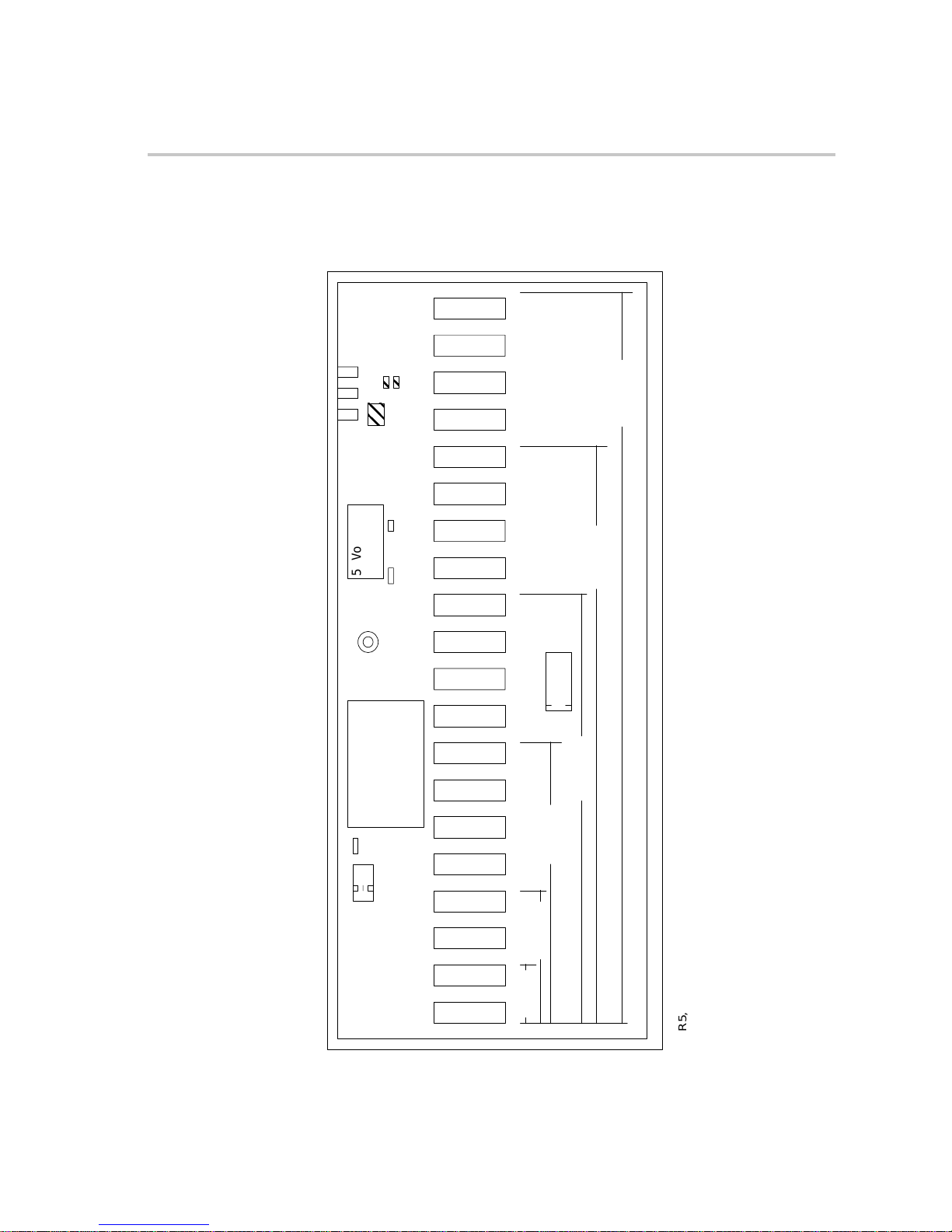
A.2 Board Layouts and Schematics
Figure A–1. Backplane Layout, Front Side
LED 3
R6
R5
LED 2
LED 1
P1–20
P1–19
P1–18
P1–17
Board Layouts and Schematics
Group 1
U2
JP1
5 Volts @
1 Amp.
F1
J5
3.3 Volts @ 7.5
Amps.
F2
U1
P1–16
P1–15
P1–14
P1–13
P1–12
P1–11
P1–10
P1–9
P1–8
P1–7
P1–6
P1–5
P1–4
Group 2
P3
Group 3
Group 4
P1–3
P1–2
P1–1
Group 5
Group 6
U2, R5, and R6 are not installed at this time.
A-5Bill of Materials, Schematics, Board Layouts, and Suggested Specifications
Page 77

Board Layouts and Schematics
Figure A–2. Backplane Layout, Back Side
P1–1B
A-6
P1–20B
Page 78
Board Layouts and Schematics
Figure A–3. Driver-Card and Receiver-Card Connector Pinout
P1-X P1-1B and P1-20B
ABCDE EDCBA
1
Sys. Clk.
2 3.3V 3.3V GND 3.3V 3.3V 2 3.3V 3.3V 3.3V
3
G1D3 G1D1
4
G1D7 G1D5
5 1.5V 1.5V GND 1.5V 1.5V 5 1.5V 1.5V 1.5V 1.5V
6
G2D3 G2D1
7
G2D7 G2D5
8 GND GND GND GND GND 8 GND GND GND GND
9
G3D3 G3D1
10
G3D7 G3D5
11 GND GND GND GND GND 11 GND GND GND GND
15 GND GND GND GND GND
16
G4D3 G4D1
17
G4D7 G4D5
18 GND GND GND GND GND
19
G5D3 G5D1
20
G5D7 G5D5
21 GND GND GND GND GND
22
G6D3 G6D1
23
G6D7 G6D5
24 GND GND GND GND GND
25
MODESEL
GND GND 5V 5V 1 GND 5V
GND
GND
GND
GND
GND
GND
GND
GND
GND
GND
GND
GND
GND GND GND
G1D4 G1D2
G1D8 G1D6
G2D4 G2D2
G2D8 G2D6
G3D4 G3D2
G3D8 G3D6
G4D4 G4D2
G4D8 G4D6
G5D4 G5D2
G5D8 G5D6
G6D4 G6D2
G6D8 G6D6
GTL Clk.
3
G1D3 G1D1 G1D4 G1D2
4
G1D7 G1D5 G1D8 G1D6
6
7
9
10
GND
GND
GND
GND
GND
GND
GND
GND
GND
GND
GND
P3
ABCDE
1
Clk.Out 20
2
Clk.Out 18 Clk.Out 19
3
Clk.Out 16 Clk.Out 17
4
Clk.Out 14 Clk.Out 15
5
Clk.Out 12 Clk.Out 13
6
Clk.Out 10 Clk.Out 11
7
Clk.Out 8 Clk.Out 9
8
Clk.Out 6 Clk.Out 7
9
Clk.Out 4 Clk.Out 5
10
Clk.Out 2 Clk.Out 3
11
Clk.Out 1
GND GND
GND GND
GND GND
GND GND
GND GND
GND 5V
GND GND
GND GND
GND GND
GND 3.3V
GND GND 3.3V
GND
GND
GND
GND
GND
GND
GND
GND
GND
GND
GND
MODESEL
A-7Bill of Materials, Schematics, Board Layouts, and Suggested Specifications
Page 79

Board Layouts and Schematics
Figure A–4. Backplane Schematic
A-8
Page 80

Board Layouts and Schematics
A-9Bill of Materials, Schematics, Board Layouts, and Suggested Specifications
Figure A–5. Driver-Card Layout
4.0 inches
3.0 inches
AMP type A 100623–1
OUTPUT Connector
J1–x
column 1
.76 inch
GTLxxx
GTLxxxGTLxxx
U1U2
U3
SMB
SMB
SMB
SMB
SMB
SMB
TP1
TP2
TP3
TP4
TP5
TP6
GP1
GP2
GP3
GP4
GP5
GP6
SMB
SMB
TP8 TP7
CLK
DATA
ALVCH16344ALVCH16344
U4U5
CDC351
U6
LVC112A
U7
LVC112A
LVC112A
U8U9
ALVC04
U12
PCJ1
GTLP1394
ALVC126
U10
U11
PCJ2
Jumper Block 2
1
2
R1
R2
R3
R4
R5R6
R7
R8
R9
R11
R12
R13
C1
C2
C3
C4
C5
C6
C7
C8
C9
C10
C11
C12
C13
C14
C15
C16
C17
C18
C19
C21
C20
R9
C22
2
3
1
R10
Jumper Block 1
1
2
R14
Jumper Block 3
Page 81

Board Layouts and Schematics
Figure A–6. Driver-Card Schematic
A-10
Page 82

Board Layouts and Schematics
A-11Bill of Materials, Schematics, Board Layouts, and Suggested Specifications
Figure A–7. Unmonitored-Receiver Card Layout
3.5 inches
3 inches
OUTPUT Connector
AMP type A 100623–1
J1–x
column 1
U1
U2
U3
GTL 1655GTL 1655
GTL 1655
U5
ALVCH126
U4
R1
C1
R2
C8
C9
C10
C11
C12
C13
C14
C15
C16
C17
RECEIVER CARD
(Standard)
RTerm RTerm
RTerm
RTerm RTerm RTerm
GTLP1394
.76 inch
C18
Page 83

Board Layouts and Schematics
A-12
Figure A–8. Monitored-Receiver Card Layout
3.5 inches
3 inches
OUTPUT Connector
AMP type A 100623–1
J1–x
TP1
TP2
TP3
TP4
TP5
TP6
TP7
TP8
TP9TP10
TP11
TP12
GP1
GP2
GP3
GP4
GP5
GP6
GP1GP2
GP3GP4
GP5
GP6
column 1
U1
U2
U3
GTL 1655GTL 1655
GTL 1655
U5
ALVCH126
U4
R1
C1
R2
R3
R4
R5R6
R7
R8
R9
R10R11
R12
R13
R14
C2
C3C4C5
C6
C7
C8
C9
C10
C11
C12
C13
C14
C16
C17
SMB SMB SMB
SMB SMB
SMB
SMB
SMB
SMB
SMB
SMB
SMB
RECEIVER CARD (Monitor)
10K network
10K network 10K network
10K network
10K network 10K network
RTerm RTerm RTerm
RTerm RTerm
RTerm
SMB
TP13
CLK
GTLP1394
R15
.76 inch
C15
C18
Page 84

Figure A–9. Receiver-Card Schematic
Board Layouts and Schematics
A-13Bill of Materials, Schematics, Board Layouts, and Suggested Specifications
Page 85

Board Layouts and Schematics
A-14
Figure A–10. Clock-Card Layout
2.5 inches
2.5 inches
OUTPUT Connector
CLOCK
CLOCK DRIVER
SMB
Monitor
AMP type C
100161–1
CLOCK
CARD
TP1
U1
U2
R1
J3
C1
C3
C2
C4
C5
CLOCK DRIVER
U3
C6
C7
C8
C9
column 1
.76 inch
C10
Page 86

Board Layouts and Schematics
A-15Bill of Materials, Schematics, Board Layouts, and Suggested Specifications
Figure A–11. Clock-Card Schematic
Clock Card
A
11
Thursday, March 16, 2000
Title
Size Document Number
Rev
Date: Sheet of
3.3V 3.3V
3.3V
5V
3.3V
51.1
U1
TP1
R1
C1
.1uF
U2 U3
C3
.1uF .1uF
.1uF
C4
C5
.1uF
.1uF .1uF
.1uF
.1uF
C6 C7
C8
C9
J3
50 ohm lines. All clock
output lines to J3 are
the same length (5%)
C10
.1uF
R2
453
CLK_OUT1
CLK_OUT6
CLK_OUT9
CLK_OUT10
CLK_OUT16
CLK_OUT18
CLK_OUT4
CLK_OUT7
CLK_OUT15
CLK_OUT2
CLK_OUT5
CLK_OUT17
CLK_OUT19
CLK_OUT13
CLK_OUT3
CLK_OUT20
CLK_OUT8
CLK_OUT12
CLK_OUT11
CLK_OUT14
CDC2586
GND
1
1Y1
2
Vcc
3
GND
4
1Y2
5
Vcc
6
GND
7
1Y3
8
Vcc
9
GND
10
GND
11
2Y1
12
Vcc
13
GND
3Y3
Vcc
GND
GND
4Y1
Vcc
GND
4Y2
Vcc
GND
4Y3
Vcc
CLR
TESTOEVccNCCLKIN
Vcc
GND
FBIN
GND
SEL0
SEL1
GND
CDC2586
GND
1
1Y1
2
Vcc
3
GND
4
1Y2
5
Vcc
6
GND
7
1Y3
8
Vcc
9
GND
10
GND
11
2Y1
12
Vcc
13
GND
14
2Y2
15
Vcc
16
GND
17
2Y3
18
Vcc
19
GND20GND
21
3Y1
22
Vcc
23
GND
24
3Y2
25
Vcc
26
GND
27
3Y3
28
Vcc
29
GND
30
GND
31
4Y1
32
Vcc
33
GND
34
4Y2
35
Vcc
36
GND
37
4Y3
38
Vcc
39
CLR40TEST41OE42Vcc43NC44CLKIN45Vcc46GND47FBIN48GND49SEL050SEL151GND
52
Z– PAK (C)
C1C2C3C4C5C6C7C8C9
C10
C11
D1D2D3D4D5D6D7D8D9
D10
D11
E3E2E4E5E6
E7
E8E9E10
E11B1B11
E1
A1
A2
A3
A4
A5
A6
A7
A8
A9
A10
A11
B2
B3
B4
B5
B6
B7
B8
B9
B10
OSC
N/C
1
GND
4
OUT
5
Vcc
8
SMB
1
324
5
GND
2Y2
Vcc
GND
2Y3
Vcc
GND
GND
3Y1
Vcc
GND
3Y2
Vcc
40
41
42
43
44
45
46
47
48
49
50
51
52
14
15
16
17
18
19
20
21
22
23
24
25
26
27
28
29
30
31
32
33
34
35
36
37
38
39
Page 87

Board Layouts and Schematics
A-16
Figure A–12. Resistor-Termination-Card Layout
Output Connector
AMP type C
100161–1
column 1
1.5 inch
2 inch
R1
R2
R3
R4
R5
R6 R7
R8
C1
C2
C3
C4
J4
Standard termination card
Page 88

Board Layouts and Schematics
A-17Bill of Materials, Schematics, Board Layouts, and Suggested Specifications
Figure A–13. Standard-Termination-Card Schematic
T ermination Card
A
11Wednesday, December 08, 1999
Title
Size Document Number
Rev
Date: Sheet of
R7
R3
R5
R1
R6
R4
C1 C2
C3
C4
J4
R8
R2
G1D2G1
D4
G1
D1
G1
D3
G1D6G1
D8
G1
D5
G1
D7
1.5
Z– PAK (C)
C1C2C3C4C5C6C7C8C9
C10C1
1
D1D2D3D4D5D6D7D8D9
D10D1
1
E3E2E4E5E6E7
E8E9
E10E1
1
B1
B1
1
E1 A1A2A3A4A5A6A7A8A9
A10A1
1
B2B3B4B5B6B7B8B9
B1
0
Page 89

Board Layouts and Schematics
A-18
 Loading...