

®
DRV1100
DRV1100
OPA658
DRV1100
HIGH POWER DIFFERENTIAL DRIVER AMPLIFIER
FEATURES
● HIGH OUTPUT CURRENT: 230mA
● SINGLE SUPPLY OPERATION: 5V
● 5MHz BANDWIDTH: 6Vp-p into 15Ω
● VERY LOW THD AT HIGH POWER:
–72dBc at 6Vp-p, 100kHz, 100Ω
● LOW QUIESCENT CURRENT: 11mA
● FIXED DIFFERENTIAL GAIN: 3V/V
APPLICATIONS
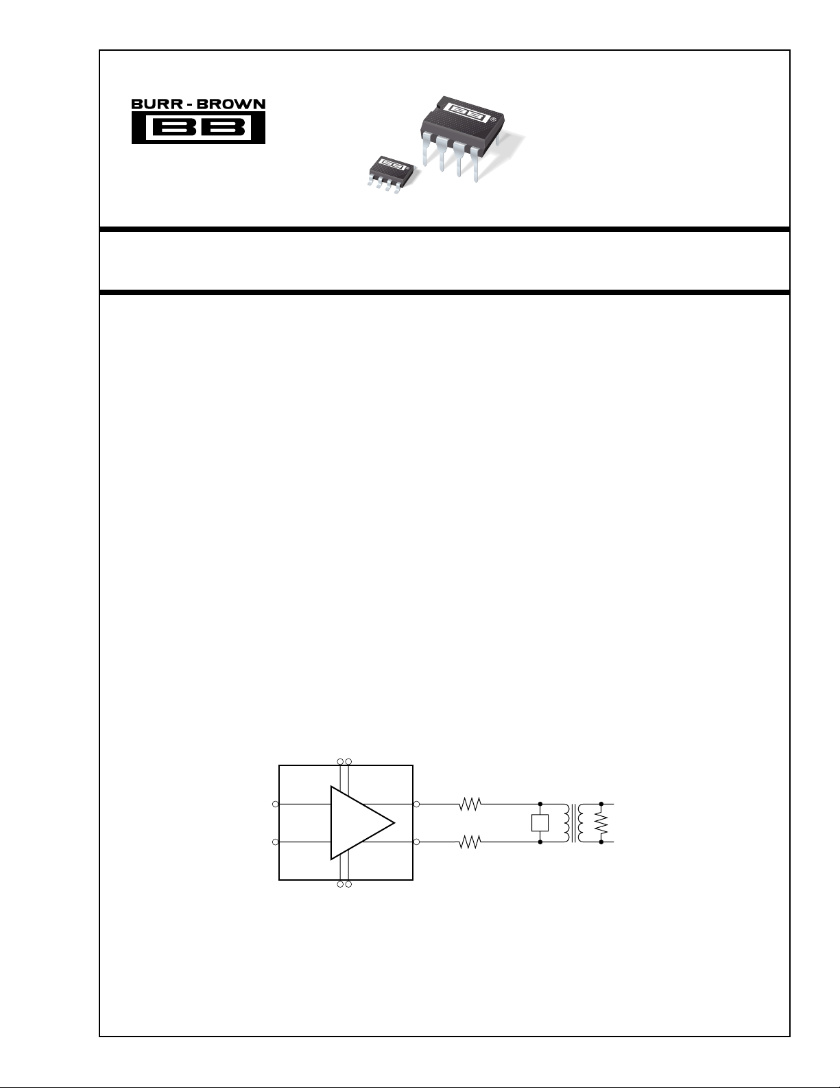
● xDSL TWISTED PAIR LINE DRIVER
● COMMUNICATIONS LINE DRIVER
● TRANSFORMER DRIVER
● SOLENOID DRIVER
● HIGH POWER AUDIO DRIVER
● CRT YOKE DRIVER
DESCRIPTION
The DRV1100 is fixed gain differential line driver
designed for very low harmonic distortion at the high
powers required of xDSL line interface standards.
Operating on a single +5V supply, it can deliver
230mA peak output current and 9.5Vp-p differential
output voltage swing. This high output power on a
single +5V supply makes the DRV1100 an excellent
choice for the xDSL applications that require up to
17dBm power onto the line with high crest factors.
The DRV1100 is available in both 8-pin plastic DIP
and SO-8 packages.
SBWS004
+5V
DRV1100
4Ω
In+
G = 3V/V
In–
Patent
Pending
GND
International Airport Industrial Park • Mailing Address: PO Box 11400, Tucson, AZ 85734 • Street Address: 6730 S. Tucson Blvd., Tucson, AZ 85706 • Tel: (520) 746-1111 • Twx: 910-952-1111
Internet: http://www.burr-brown.com/ • FAXLine: (800) 548-6133 (US/Canada Only) • Cable: BBRCORP • Telex: 066-6491 • FAX: (520) 889-1510 • Immediate Product Info: (800) 548-6132
©
1996 Burr-Brown Corporation PDS-1354 Printed in U.S.A. December, 1996
Out+
Out–
4Ω
Protection
135Ω
1:4
Transformer

SPECIFICATIONS
At VDD = +5.0V, VCM = VDD/2, TA = 25°C, unless otherwise specified.
DRV1100P, U
PARAMETER CONDITIONS MIN TYP MAX UNITS
AC PERFORMANCE
–3dB Bandwidth R
Differential Slew Rate R
Step Response Delay
(1)
Settling Time to 1%, Step Input V
Settling Time to 1%, Step Input V
Settling Time to 0.1%, Step Input V
Settling Time to 0.1%, Step Input V
THD, Total Harmonic Distortion
(2)
f = 10kHz RL = 100Ω, VO = 6Vp-p –85 dBc
f = 10kHz R
f = 100kHz R
f = 100kHz R
Input Voltage Noise f = 100kHz 30 nV/√Hz
Input Current Noise f = 100kHz 0.5 fA/√Hz
INPUT CHARACTERISTICS
Differential Input Resistance 10
Differential Input Capacitance 1pF
Common-Mode Input Resistance 10
Common-Mode Input Capacitance 6pF
Input Offset Voltage 5mV
Input Bias Current 1pA
Common-Mode Rejection Ratio Input Referred 62 dB
Power Supply Rejection Ratio Input Referred 60 76 dB
Input Common-Mode Voltage Range
(3)
OUTPUT CHARACTERISTICS
Differential Output Offset, RTO 10 25 mV
Differential Output Offset Drift, RTO –40°C to +85°C30µV/°C
Differential Output Resistance 0.16 Ω
Peak Current (Continuous) R
Differential Output Voltage Swing R
Output Voltage Swing, Each Side R
Gain Fixed Gain, Differential 3 V/V
Gain Error ±0.25 dB
POWER SUPPLY
Operating Voltage Range +4.5 +5.0 +5.5 V
Quiescent Current V
TEMPERATURE RANGE –40 +85 °C
Thermal Resistance,
DRV1100P 8-Pin DIP 100 °C/W
θ
JA
DRV1100U 8-Pin SO-8 125 °C/W
NOTES: (1) Time from 50% point of input step to 50% point of output step. (2) Measurement Bandwidth = 500kHz. (3) Output common-mode voltage follows input
common-mode voltage; therefore, if input V
= VDD/2, then output VCM = VDD/2.
CM
= 15Ω, VO = 1Vp-p 8 MHz
L
R
≥ 100Ω, VO = 1Vp-p 11 MHz
L
R
= 15Ω, VO = 6Vp-p 5 MHz
L
R
≥ 100Ω, VO = 6Vp-p 6 MHz
L
= 100Ω, VO = 6Vp-p 80 V/µs
L
VO = 1Vp-p 25 ns
= 1Vp-p, RL = 100Ω 0.25 µs
O
= 6Vp-p, RL = 100Ω 0.3 µs
O
= 1Vp-p, RL = 100Ω 0.8 µs
O
= 6Vp-p, RL = 100Ω 1.1 µs
O
= 15Ω, VO = 6Vp-p –66 –76 dBc
L
= 100Ω, VO = 6Vp-p –72 dBc
L
= 15Ω, VO = 6Vp-p –65 dBc
L
11
11
0.5 VDD –0.5 V
= 15Ω 200 230 mA
L
= 1kΩ 9.6 Vp-p
L
R
= 100Ω 8.5 9.5 Vp-p
L
R
= 15Ω 6.0 6.6 Vp-p
L
= 1kΩ 0.125 4.875 V
L
= 5.0V +11 +16 mA
DD
Ω
Ω
The information provided herein is believed to be reliable; however, BURR-BROWN assumes no responsibility for inaccuracies or omissions. BURR-BROWN
assumes no responsibility for the use of this information, and all use of such information shall be entirely at the user’s own risk. Prices and specifications are subject
to change without notice. No patent rights or licenses to any of the circuits described herein are implied or granted to any third party. BURR-BROWN does not
authorize or warrant any BURR-BROWN product for use in life support devices and/or systems.
®
DRV1100
2
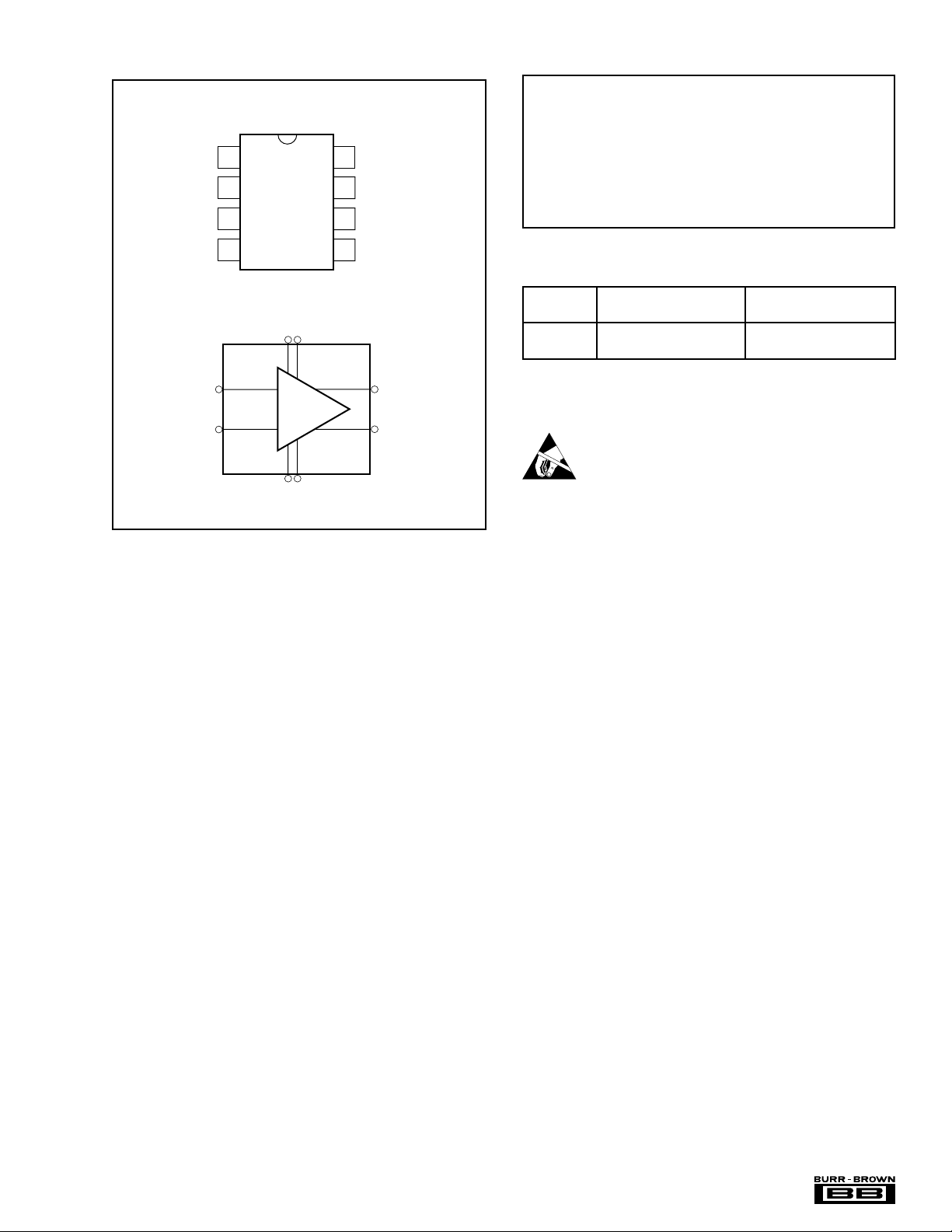
PIN CONFIGURATIONS
Top View
1
GND
2
In+
3
In–
ABSOLUTE MAXIMUM RATINGS
Analog Inputs: Current .............................................. ±100mA, Momentary
Analog Outputs Short Circuit to Ground (+25°C) ..................... Momentary
8
Out–
7
V
(+5V)
DD
6
V
(+5V)
DD
Analog Outputs Short Circuit to V
V
to GND .............................................................................. –0.3V to 6V
DD
Junction Temperature ................................................................... +150°C
Storage Temperature Range .......................................... –40°C to +125°C
Lead Temperature (soldering, 3s)................................................. +260°C
Power Dissipation .............................. (See Thermal/Analysis Discussion)
Voltage....................................... GND –0.3V to V
(+25°C) ........................... Momentary
DD
±10mA, Continuous
DD
+0.2V
GND
In+
In–
4
5
Out+
PACKAGE/ORDERING INFORMATION
PRODUCT PACKAGE NUMBER
+5V
67
2
3
5
Out+
8
Out–
DRV1100P 8-Pin PDIP 006
DRV1100U 8-Lead SO-8 182
NOTE: (1) For detailed drawing and dimension table, please see end of data
sheet, or Appendix C of Burr-Brown IC Data Book.
PACKAGE DRAWING
(1)
ELECTROSTATIC
41
GND
This integrated circuit can be damaged by ESD. Burr-Brown
recommends that all integrated circuits be handled with
appropriate precautions. Failure to observe proper handling
and installation procedures can cause damage.
ESD damage can range from subtle performance degradation
to complete device failure. Precision integrated circuits may
be more susceptible to damage because very small parametric
changes could cause the device not to meet its published
specifications.
DISCHARGE SENSITIVITY
®
3
DRV1100
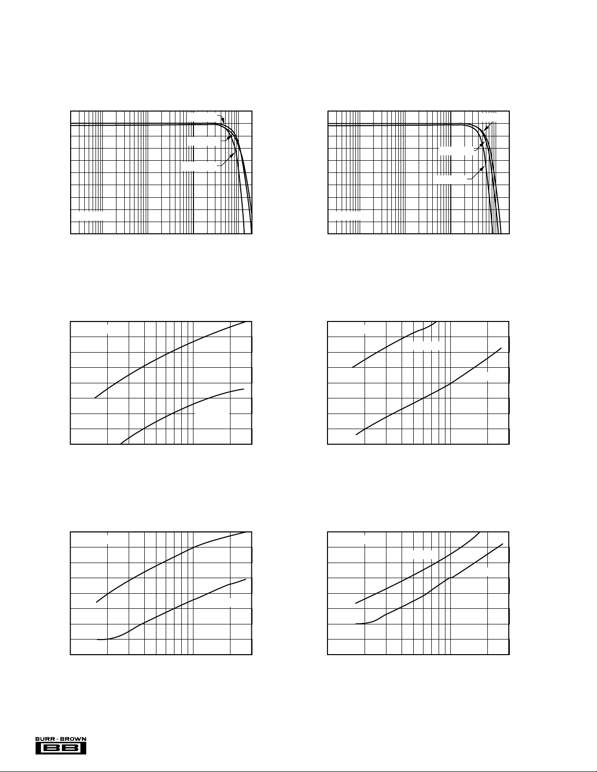
TYPICAL PERFORMANCE CURVES
At VDD = +5.0V, VCM = VDD/2, TA = 25°C, unless otherwise specified.
SMALL SIGNAL FREQUENCY RESPONSE
9.5
8.5
7.5
6.5
5.5
4.5
3.5
Differential Gain (dB)
2.5
VO = 1Vp-p
1.5
10K 100K
–40
–45
–50
–55
–60
–65
2nd Harmonic (dB)
–70
–75
–80
SMALL SIGNAL 2ND HARMONIC DISTORTION
VO = 1Vp-p
100K
Frequency (Hz)
Frequency (Hz)
RL = 1kΩ
RL = 100Ω
RL = 15Ω
1M 10M
RL = 15Ω
RL = 100Ω
1M 10M
LARGE SIGNAL FREQUENCY RESPONSE
9.5
8.5
7.5
6.5
5.5
4.5
3.5
Differential Gain (dB)
2.5
VO = 6Vp-p
1.5
10K 100K
–40
–45
–50
–55
–60
–65
3rd Harmonic (dB)
–70
–75
–80
SMALL SIGNAL 3RD HARMONIC DISTORTION
VO = 1Vp-p
100K
RL = 1kΩ
RL = 100Ω
RL = 15Ω
1M 10M
Frequency (Hz)
RL = 15Ω
RL = 100Ω
1M 10M
Frequency (Hz)
–40
–45
–50
–55
–60
–65
2nd Harmonic (dB)
–70
–75
–80
LARGE SIGNAL 2ND HARMONIC DISTORTION
VO = 6Vp-p
100K
®
Frequency (Hz)
DRV1100
RL = 15Ω
RL = 100Ω
1M 10M
4
–40
–45
–50
–55
–60
–65
3rd Harmonic (dB)
–70
–75
–80
LARGE SIGNAL 3RD HARMONIC DISTORTION
VO = 6Vp-p
100K
RL = 15Ω
RL = 100Ω
1M 10M
Frequency (Hz)

TYPICAL PERFORMANCE CURVES (CONT)
–40
–50
–60
–70
–80
–90
1234
100kHz THD
THD (dBc)
Differential Output Voltage (Vp-p)
5678910
RL = 15Ω
RL = 100Ω
RL = 1kΩ
+3V
0
–3V
LARGE SIGNAL STEP RESPONSE
Differential Voltage (750mV/div)
Time (50ns/div)
Output
Input
RL = 100Ω
At VDD = +5.0V, VCM = VDD/2, TA = 25°C, unless otherwise specified.
–40
–50
–60
–70
THD (dBc)
–80
–90
1234
Differential Output Voltage (Vp-p)
SMALL SIGNAL STEP RESPONSE
+0.5V
0
10kHz THD
RL = 15Ω
RL = 100Ω
RL = 1kΩ
Output
Input
5678910
RL = 100Ω
Differential Voltage (125mV/div)
–0.5V
Time (50ns/div)
10
9
8
7
6
5
4
3
2
Differential Output Swing (Vp-p)
1
0
LARGE SIGNAL OPERATING RANGE
10K1K 100K
Frequency (Hz)
RL = 100Ω1% THD
RL = 15Ω
RL = 1kΩ
1M 10M
12
10
8
6
4
2
Differential Output Voltage (Vp-p)
0
4.5 4.75 5 5.25 5.5
MAXIMUM V
vs SUPPLY VOLTAGE
O
Supply Voltage (VDD)
RL = 1kΩ
RL = 100Ω
RL = 15Ω
®
5
DRV1100

TYPICAL PERFORMANCE CURVES (CONT)
At VDD = +5.0V, VCM = VDD/2, TA = 25°C, unless otherwise specified.
1000
100
Voltage Noise (nV/√Hz)
10
100 1K 10K 100K 1M
13
12
11
10
9
8
7
6
Quiescent Current (mA)
5
4
3
–40 –20 0 20 40 60 80 100
DIFFERENTIAL INPUT VOLTAGE NOISE
Frequency (Hz)
QUIESCENT CURRENT vs TEMPERATURE
VDD = +5V
Temperature (°C)
DIFFERENTIAL OUTPUT IMPEDANCE
10
1
Impedance (Ω)
0.1
1k 10K 100K 1M 10M
Frequency
80
70
60
50
40
PSRR (dB)
30
20
10
POWER SUPPLY REJECTION vs FREQUENCY
0
10K1K 100K
Frequency (Hz)
1M 10M
®
DRV1100
6

APPLICATIONS INFORMATION
INTERNAL BLOCK DIAGRAM
The DRV1100 is a true differential input to differential
output fixed gain amplifier. Operating on a single +5V
power supply, it provides an internally fixed differential
gain of +3 and a common-mode gain of +1 from the input to
output. Fabricated on an advanced CMOS process, it offers
very high input impedance along with a low impedance
230mA output drive. Figure 1 shows a simplified internal
block diagram.
Out+
In+
Buffer
Preamp
Out–
In–
Out+
V
V
DD
Out–
V
DD
Load
/2
/2
0V
P
V
P
V
P
V
P
FIGURE 2. DRV1100 Single Ended and Differential Output
Waveforms.
(Vp-p). Squaring 1/2 of the Vp-p and dividing by the load
will give the peak power. For example, the Typical Performance Curves show that on +5V supply the DRV1100 will
deliver 6.8Vp-p into 15Ω at 500kHz. The peak load power
under this condition is (6.8Vp-p/2)2/15Ω = 770mW.
FIGURE 1. Simplified DRV1100 Internal Block Diagram.
To achieve the maximum dynamic range, operate the
DRV1100 with the inputs centered at VDD/2. This will place
the output differential swing centered at VDD/ 2 for maximum swing and lowest distortion. Purely differential input
signals will produce a purely differential output signal. A
single ended input signal, applied to one input of the
DRV1100, with the other input at a fixed voltage, will
produce both a differential and common-mode output signal.
This is an acceptable mode of operation when the DRV1100
is driving an element with good common-mode rejection
(such as a transformer).
DIFFERENTIAL OUTPUT VOLTAGE AND POWER
Applying the balanced differential output voltage of the
DRV1100 to a load between the outputs will produce a peakto-peak voltage swing that is twice the swing of each
individual output. This is illustrated in Figure 2 where the
common-mode voltage is VDD/2. For a load connected
between the outputs, the only voltage that matters is the
differential voltage between the two outputs—the commonmode voltage does not produce any load current in this case.
The peak power that the DRV1100 can deliver into a
differential load is V
2
/RL. The Typical Performance Curves
P
show the maximum Vp-p versus load and frequency. The
peak voltage (Vp) equals 1/2 of the peak-to-peak voltage
SUPPLY VOLTAGE
The DRV1100 is designed for operation on a single +5V
supply. For loads > 200Ω, each output will swing rail to rail.
This gives a peak-to-peak differential output swing that is
approximately = 2 • VDD. For best distortion performance,
the power supply should be decoupled to a good ground
plane immediately adjacent to the package with a 0.1µF
capacitor. In addition, a larger electolytic supply decoupling
capacitor (6.8µF) should be near the package but can be
shared among multiple devices.
DIGITAL SUBSCRIBER LINE APPLICATIONS
The DRV1100 is particularly suited to the high power, low
distortion, requirements of a twisted pair driver in digital
communications applications. These include HDSL (High
bit rate Digital Subscriber Lines), ADSL (Asymmetrical
Digital Subscriber Lines), and RADSL (Rate adaptive ADSL).
Figure 3 shows a typical transformer coupled xDSL line
driver configuration. In general, the DRV1100 is usable for
output power requirements up to 17dBm with a crest factor
up to 6 (crest factor is the ratio of peak to rms voltage).
To calculate the required amplifier power for an xDSL
application—
• Determine the average power required onto the line in the
particular application. The DRV1100 must be able to
deliver twice this power (+3dB) to account for the power
®
7
DRV1100

+5V
DRV1100
In+
In–
GND
Out+
Out–
FIGURE 3. Typical Digital Subscriber Line Application.
4Ω
4Ω
Protection Circuits
Line Impedance
135Ω
1:4
Transformer
loss through the series impedance matching resistors shown
in Figure 3. Twice the required line power must be
delivered by the DRV1100 through the frequency band
of interest with the distortion required by the system.
• Calculate the RMS voltage required at the output of the
DRV1100 with this 2X line power requirement. Vrms =
(2 • P
LINE
• RL)
1/2
, where RL is the total load impedance
that the DRV1100 must drive. Multiply this Vrms by 2 •
crest factor to get the total required differential peak-topeak voltage at the output. The DRV1100 must be able
to drive the peak-to-peak differential voltage into the
load impedance.
Where possible, the transformer turns ratio may be adjusted
to keep within the DRV1100 output voltage and current
constraints for a given R
and desired power onto the
LINE
line.
Using the example of Figure 3, assume the average power
desired on a 135Ω line is 14dBm (HDSL). Twice this power
(17dBm) is required into the matching resistors on the
primary side of the transformer. This 135Ω load is reflected
through the 1:4 transformer as a (135/(42)) = 8.4Ω load. The
two series 4.1Ω resistors, along with the 0.2Ω differential
output impedance of the DRV1100, will provide impedance
matching into this 8.4Ω load. The DRV1100 will see approximately a 16.5Ω load under these conditions. The required 17dBm (50mW) into this load will need an output
Vrms = (50mW • 16.5)
1/2
= 0.91Vrms. Assuming a crest
factor of 3, the differential peak-to-peak output voltage = 6
• 0.91 = 5.45Vp-p. The Typical Performance Curves show
that, at 100kHz, the DRV1100 can deliver this voltage swing
with less than –62dB THD.
OUTPUT PROTECTION
Figure 3 also shows overvoltage and short circuit protection
elements that are commonly included in xDSL applications.
Overvoltage suppressors include diodes or MOV’s. The
outputs of the DRV1100 can be momentarily shorted to
ground or to the supply without damage. The outputs are not,
however, designed for a continuous short to ground or the
supply.
POWER DISSIPATION AND THERMAL ANALYSIS
The total internal power dissipation of the DRV1100 is the
sum of a quiescent term and the power dissipated internally
to deliver the load power. The Typical Performance Curves
show the quiescent current over temperature. At +5V supply, the typical no load supply current of 11mA will dissipate 55mW quiescent power. The rms power dissipated in
the output circuit to deliver a Vrms to a load RL is:
Prms = (VDD – Vrms) • (Vrms/RL)
The internal power dissipation will reach a maximum when
Vrms is equal to VDD/2. For a sinusoidal output, this
corresponds to an output Vp-p = 1.41 • VDD.
As an example, compute the power and junction temperature
under a worst case condition with VDD = +5V and Vrms =
2.5V into a 16Ω differential load (peak output current for a
sinusoid would be 222mA). The total internal power dissipation would be:
(5V • 11mA) + (5V – 2.5V) • (2.5V/16Ω) = 446mW
To compute the internal junctions temperature, this power is
multiplied by the junction to ambient thermal impedance (to
get the temperature rise above ambient) then added to the
ambient temperature. Using the specified maximum ambient
temperature of +85°C, the junction temperature for the
DRV1100 in an SO-8 package under these worst case
conditions will be:
TJ = 85°C + 0.446W • 125°C/W = 141°C
®
DRV1100
8

INTERNAL TEMPERATURE RISE
90
80
Limit at 85°C Ambient
70
60
50
40
30
Temperature Rise
20
10
0
0 0.5 1 1.5
OF DRV1100 IN SOIC
RL = 15Ω
RL = 100Ω
2 2.5 3 3.5
Load Voltage (rms)
FIGURE 4. Junction Temperature Rise From Ambient for
the DRV1100U.
The internal junction temperature should, in all cases, be
limited to < 150°C. For a maximum ambient temperature of
+85°C, this limits the internal temperature rise to less than
65°C. Figure 4 shows the temperature rise from ambient to
junction for loads of 15Ω and 100Ω. This shows that the
internal junction temperature will never exceed the rated
maximum for a 15Ω load.
INPUT INTERFACE CIRCUITS
Best performance with the DRV1100 is achieved with a
differential input centered at VDD/2. Signals that do not
require DC coupling may be connected as shown in Figure
5 through blocking caps to a midpoint reference developed
through resistor dividers from the supply voltage. The value
for the RB resistors determine four performance requirements.
• They bias the inputs at the supply midpoint.
• They provide a DC bias current path for the input to the
DRV1100
• They set the AC input impedance for the source signals to
RB/2.
• They set the low frequency cutoff frequency along with
CB.
+V
DD
Often, the RB resistors will be set to a relatively high value
(> 10kΩ) to minimize quiescent current in the reference
path. If a lower input impedance is desired, additional
terminating resistors may be added to the input side of the
blocking capacitors (CB).
The circuit of Figure 5 may also be operated with only a
single ended input. In that case, the reference voltage on the
other input should be decoupled to ground with a 0.1µF
capacitor. In this connection, the input will generate unbalanced outputs. The differential output voltage will still be
3 times the input peak-to-peak voltage, but since there is
now a common-mode voltage input, there will be a common
mode voltage output. The output common-mode voltage
will be equal to the input signal’s peak-to-peak swing. This
common-mode component will reduce the available differential output voltage swing. However, if the output load has
good common-mode rejection, such as a transformer, this is
an acceptable way of using the DRV1100 with a single
ended source.
Figure 6 shows a means of translating a ground centered
single ended input to a purely differential signal for application to DRV1100 input. This circuit uses a wideband dual op
amp in cross coupled feedback configuration.
The outputs of this circuit may then be fed into the inputs of
Figure 5. The total gain of Figure 6 is 2 • (RF/RG). The
circuit will act to hold all 4 op amp inputs equal to the
+ input of the lower op amp. Since this is at ground, the
midpoint for the input signal (where the two outputs will be
equal) is also at 0V.
R
F
R
G
V
I
R
F
+ V
R
G
I
500Ω
1/2
OPA2650
500Ω
500Ω
500Ω
R
R
B
B
DRV1100
R
C
V
1
V
2
B
R
B
C
B
R
B
FIGURE 5. AC Coupled Differential Input Interface.
1/2
OPA2650
L
R
F
– V
R
G
I
FIGURE 6. Single Ended to Differential Conversion.
®
9
DRV1100

PACKAGE OPTION ADDENDUM
www.ti.com
11-Nov-2008
PACKAGING INFORMATION
Orderable Device Status
(1)
Package
Type
Package
Drawing
Pins Package
Qty
Eco Plan
DRV1100U NRND SOIC D 8 75 Green (RoHS &
no Sb/Br)
DRV1100U/2K5 NRND SOIC D 8 2500 Green (RoHS &
no Sb/Br)
DRV1100U/2K5G4 NRND SOIC D 8 2500 Green (RoHS &
no Sb/Br)
DRV1100UG4 NRND SOIC D 8 75 Green (RoHS &
no Sb/Br)
(1)
The marketing status values are defined as follows:
ACTIVE: Product device recommended for new designs.
LIFEBUY: TI has announced that the device will be discontinued, and a lifetime-buy period is in effect.
NRND: Not recommended for new designs. Device is in production to support existing customers, but TI does not recommend using this part in
a new design.
PREVIEW: Device has been announced but is not in production. Samples may or may not be available.
OBSOLETE: TI has discontinued the production of the device.
(2)
Eco Plan - The planned eco-friendly classification: Pb-Free (RoHS), Pb-Free (RoHS Exempt), or Green (RoHS & no Sb/Br) - please check
http://www.ti.com/productcontent for the latest availability information and additional product content details.
TBD: The Pb-Free/Green conversion plan has not been defined.
Pb-Free (RoHS): TI's terms "Lead-Free" or "Pb-Free" mean semiconductor products that are compatible with the current RoHS requirements
for all 6 substances, including the requirement that lead not exceed 0.1% by weight in homogeneous materials. Where designed to be soldered
at high temperatures, TI Pb-Free products are suitable for use in specified lead-free processes.
Pb-Free (RoHS Exempt): This component has a RoHS exemption for either 1) lead-based flip-chip solder bumps used between the die and
package, or 2) lead-based die adhesive used between the die and leadframe. The component is otherwise considered Pb-Free (RoHS
compatible) as defined above.
Green (RoHS & no Sb/Br): TI defines "Green" to mean Pb-Free (RoHS compatible), and free of Bromine (Br) and Antimony (Sb) based flame
retardants (Br or Sb do not exceed 0.1% by weight in homogeneous material)
(2)
Lead/Ball Finish MSL Peak Temp
CU NIPDAU Level-2-260C-1 YEAR
CU NIPDAU Level-2-260C-1 YEAR
CU NIPDAU Level-2-260C-1 YEAR
CU NIPDAU Level-2-260C-1 YEAR
(3)
(3)
MSL, Peak Temp. -- The Moisture Sensitivity Level rating according to the JEDEC industry standard classifications, and peak solder
temperature.
Important Information and Disclaimer:The information provided on this page represents TI's knowledge and belief as of the date that it is
provided. TI bases its knowledge and belief on information provided by third parties, and makes no representation or warranty as to the
accuracy of such information. Efforts are underway to better integrate information from third parties. TI has taken and continues to take
reasonable steps to provide representative and accurate information but may not have conducted destructive testing or chemical analysis on
incoming materials and chemicals. TI and TI suppliers consider certain information to be proprietary, and thus CAS numbers and other limited
information may not be available for release.
In no event shall TI's liability arising out of such information exceed the total purchase price of the TI part(s) at issue in this document sold by TI
to Customer on an annual basis.
Addendum-Page 1

PACKAGE MATERIALS INFORMATION
www.ti.com
TAPE AND REEL INFORMATION
11-Mar-2008
*All dimensions are nominal
Device Package
DRV1100U/2K5 SOIC D 8 2500 330.0 12.4 6.4 5.2 2.1 8.0 12.0 Q1
Type
Package
Drawing
Pins SPQ Reel
Diameter
(mm)
Reel
Width
W1 (mm)
A0 (mm) B0(mm) K0 (mm) P1
(mm)W(mm)
Pin1
Quadrant
Pack Materials-Page 1

PACKAGE MATERIALS INFORMATION
www.ti.com
11-Mar-2008
*All dimensions are nominal
Device Package Type Package Drawing Pins SPQ Length (mm) Width (mm) Height(mm)
DRV1100U/2K5 SOIC D 8 2500 346.0 346.0 29.0
Pack Materials-Page 2

IMPORTANT NOTICE
Texas Instruments Incorporated and its subsidiaries (TI) reserve the right to make corrections, modifications, enhancements, improvements,
and other changes to its products and services at any time and to discontinue any product or service without notice. Customers should
obtain the latest relevant information before placing orders and should verify that such information is current and complete. All products are
sold subject to TI’s terms and conditions of sale supplied at the time of order acknowledgment.
TI warrants performance of its hardware products to the specifications applicable at the time of sale in accordance with TI’s standard
warranty. Testing and other quality control techniques are used to the extent TI deems necessary to support this warranty. Except where
mandated by government requirements, testing of all parameters of each product is not necessarily performed.
TI assumes no liability for applications assistance or customer product design. Customers are responsible for their products and
applications using TI components. To minimize the risks associated with customer products and applications, customers should provide
adequate design and operating safeguards.
TI does not warrant or represent that any license, either express or implied, is granted under any TI patent right, copyright, mask work right,
or other TI intellectual property right relating to any combination, machine, or process in which TI products or services are used. Information
published by TI regarding third-party products or services does not constitute a license from TI to use such products or services or a
warranty or endorsement thereof. Use of such information may require a license from a third party under the patents or other intellectual
property of the third party, or a license from TI under the patents or other intellectual property of TI.
Reproduction of TI information in TI data books or data sheets is permissible only if reproduction is without alteration and is accompanied
by all associated warranties, conditions, limitations, and notices. Reproduction of this information with alteration is an unfair and deceptive
business practice. TI is not responsible or liable for such altered documentation. Information of third parties may be subject to additional
restrictions.
Resale of TI products or services with statements different from or beyond the parameters stated by TI for that product or service voids all
express and any implied warranties for the associated TI product or service and is an unfair and deceptive business practice. TI is not
responsible or liable for any such statements.
TI products are not authorized for use in safety-critical applications (such as life support) where a failure of the TI product would reasonably
be expected to cause severe personal injury or death, unless officers of the parties have executed an agreement specifically governing
such use. Buyers represent that they have all necessary expertise in the safety and regulatory ramifications of their applications, and
acknowledge and agree that they are solely responsible for all legal, regulatory and safety-related requirements concerning their products
and any use of TI products in such safety-critical applications, notwithstanding any applications-related information or support that may be
provided by TI. Further, Buyers must fully indemnify TI and its representatives against any damages arising out of the use of TI products in
such safety-critical applications.
TI products are neither designed nor intended for use in military/aerospace applications or environments unless the TI products are
specifically designated by TI as military-grade or "enhanced plastic." Only products designated by TI as military-grade meet military
specifications. Buyers acknowledge and agree that any such use of TI products which TI has not designated as military-grade is solely at
the Buyer's risk, and that they are solely responsible for compliance with all legal and regulatory requirements in connection with such use.
TI products are neither designed nor intended for use in automotive applications or environments unless the specific TI products are
designated by TI as compliant with ISO/TS 16949 requirements. Buyers acknowledge and agree that, if they use any non-designated
products in automotive applications, TI will not be responsible for any failure to meet such requirements.
Following are URLs where you can obtain information on other Texas Instruments products and application solutions:
Products Applications
Amplifiers amplifier.ti.com Audio www.ti.com/audio
Data Converters dataconverter.ti.com Automotive www.ti.com/automotive
DSP dsp.ti.com Broadband www.ti.com/broadband
Clocks and Timers www.ti.com/clocks Digital Control www.ti.com/digitalcontrol
Interface interface.ti.com Medical www.ti.com/medical
Logic logic.ti.com Military www.ti.com/military
Power Mgmt power.ti.com Optical Networking www.ti.com/opticalnetwork
Microcontrollers microcontroller.ti.com Security www.ti.com/security
RFID www.ti-rfid.com Telephony www.ti.com/telephony
RF/IF and ZigBee® Solutions www.ti.com/lprf Video & Imaging www.ti.com/video
Mailing Address: Texas Instruments, Post Office Box 655303, Dallas, Texas 75265
Copyright © 2008, Texas Instruments Incorporated
Wireless www.ti.com/wireless
 Loading...