

Page 1
®
D
D
C1
12
D
®
D
C
11
2
SBAS085B – JANUARY 2000 – REVISED OCTOBER 2004
Dual Current Input 20-Bit
ANALOG-TO-DIGITAL CONVERTER
DDC112
FEATURES
● MONOLITHIC CHARGE MEASUREMENT A/D
CONVERTER
● DIGITAL FILTER NOISE REDUCTION:
3.2ppm, rms
● INTEGRAL LINEARITY:
±0.005% Reading ±0.5ppm FSR
● HIGH PRECISION, TRUE INTEGRATING FUNC-
TION
● PROGRAMMABLE FULL-SCALE
● SINGLE SUPPLY
● CASCADABLE OUTPUT
APPLICATIONS
● DIRECT PHOTOSENSOR DIGITIZATION
● CT SCANNER DAS
● INFRARED PYROMETER
● PRECISION PROCESS CONTROL
● LIQUID/GAS CHROMATOGRAPHY
● BLOOD ANALYSIS
Protected by US Patent #5841310
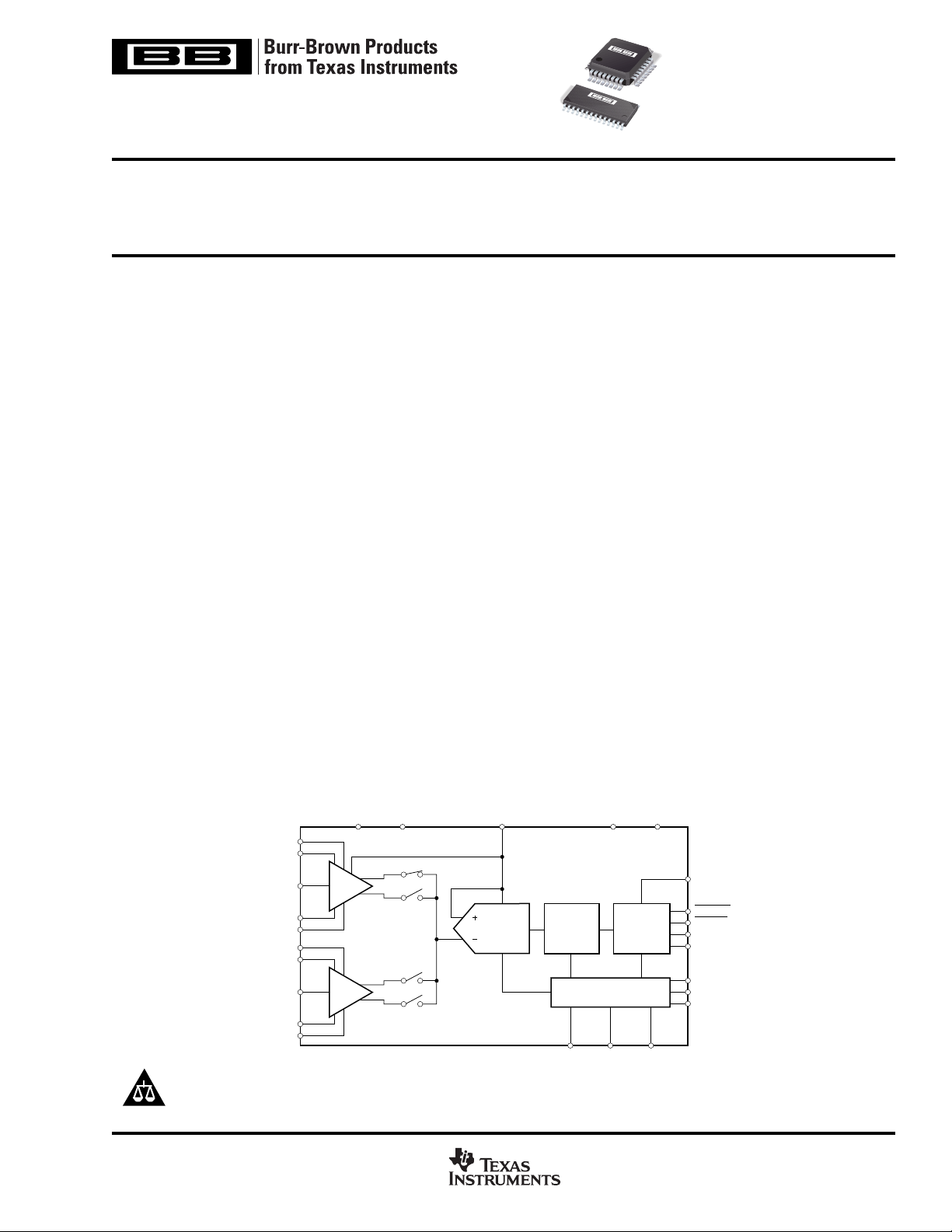
DESCRIPTION
The DDC112 is a dual input, wide dynamic range, chargedigitizing analog-to-digital (A/D) converter with 20-bit resolution. Low-level current output devices, such as photosensors,
can be directly connected to its inputs. Charge integration is
continuous as each input uses two integrators; while one is
being digitized, the other is integrating.
For each of its two inputs, the DDC112 combines current-tovoltage conversion, continuous integration, programmable
full-scale range, A/D conversion, and digital filtering to achieve
a precision, wide dynamic range digital result. In addition to
the internal programmable full-scale ranges, external integrating capacitors allow an additional user-settable full-scale
range of up to 1000pC.
To provide single-supply operation, the internal A/D converter
utilizes a differential input, with the positive input tied to V
When the integration capacitor is reset at the beginning of
each integration cycle, the capacitor charges to V
charge is removed in proportion to the input current. At the
end of the integration cycle, the remaining voltage is compared to V
REF
.
The high-speed serial shift register which holds the result of
the last conversion can be configured to allow multiple DDC112
units to be cascaded, minimizing interconnections. The
DDC112 is available in an SO-28 or TQFP-32 package and is
offered in two performance grades.
REF
REF
. This
.
AGNDAV
DD
CAP1A
CAP1A
IN1
CAP1B
CAP1B
CAP2A
CAP2A
IN2
CAP2B
CAP2B
Please be aware that an important notice concerning availability, standard warranty, and use in critical applications of
Texas Instruments semiconductor products and disclaimers thereto appears at the end of this data sheet.
All trademarks are the property of their respective owners.
PRODUCTION DATA information is current as of publication date.
Products conform to specifications per the terms of Texas Instruments
standard warranty. Production processing does not necessarily include
testing of all parameters.
CHANNEL 1
Dual
Switched
Integrator
CHANNEL 2
Dual
Switched
Integrator
V
REF
∆Σ
Modulator
www.ti.com
Digital
Filter
TEST
DGNDDV
DD
DCLK
DVALID
Digital
Input/Output
Control
CLK
CONV
Copyright © 2000-2004, Texas Instruments Incorporated
DXMIT
DOUT
DIN
RANGE2
RANGE1
RANGE0
Page 2

ABSOLUTE MAXIMUM RATINGS
AVDD to DVDD.......................................................................–0.3V to +6V
AV
to AGND ..................................................................... –0.3V to +6V
DD
DV
to DGND ..................................................................... –0.3V to +6V
DD
AGND to DGND ............................................................................... ±0.3V
V
Voltage to AGND ........................................... –0.3V to AVDD + 0.3V
REF
Digital Input Voltage to DGND .............................. –0.3V to DV
Digital Output Voltage to DGND ........................... –0.3V to DV
Package Power Dissipation ............................................. (T
Maximum Junction Temperature (T
Thermal Resistance, SO,
Thermal Resistance, TQFP,
Lead Temperature (soldering, 10s)............................................... +300°C
NOTE: (1) Stresses above those listed under
cause permanent damage to the device. Exposure to absolute maximum
conditions for extended periods may affect device reliability.
JMAX
θ
....................................................+150°C/W
JA
θ
................................................+100°C/W
JA
(1)
+ 0.3V
DD
+ 0.3V
DD
– TA)/
) ...................................... +150°C
Absolute Maximum Ratings
JMAX
θ
may
JA
ELECTROSTATIC
DISCHARGE SENSITIVITY
This integrated circuit can be damaged by ESD. Texas Instruments recommends that all integrated circuits be handled with
appropriate precautions. Failure to observe proper handling
and installation procedures can cause damage.
ESD damage can range from subtle performance degradation
to complete device failure. Precision integrated circuits may be
more susceptible to damage because very small parametric
changes could cause the device not to meet its published
specifications.
PACKAGE/ORDERING INFORMATION
MAXIMUM SPECIFICATION
PRODUCT LINEARITY ERROR RANGE PACKAGE-LEAD DESIGNATOR NUMBER
DDC112U
INTEGRAL TEMPERATURE PACKAGE ORDERING TRANSPORT
±0.025% Reading ±1.0ppm FSR
(1)
(2)
–40°C to +85°C SO-28 DW DDC112U Rails
MEDIA
"""""DDC112U/1K Tape and Reel
DDC112UK
±0.025% Reading ±1.0ppm FSR
0°C to +70°C SO-28 DW DDC112UK Rails
"""""DDC112UK/1K Tape and Reel
DDC112Y ±0.025% Reading ±1.0ppm FSR –40°C to +85°C TQFP-32 PJT DDC112Y/250 Tape and Reel
"""""DDC112Y/2K Tape and Reel
DDC112YK ±0.025% Reading ±1.0ppm FSR 0°C to +70°C TQFP-32 PJT DDC112YK/250 Tape and Reel
"""""DDC112YK/2K Tape and Reel
NOTES: (1) For the most current package and ordering information, see the Package Option Addendum located at the end of this data shee t. (2) Models with a slash
(/) are available only in Tape and Reel in the quantities indicated (/1K indicates 1000 devices per reel). Ordering 1000 pieces of
piece Tape and Reel.
DDC112U/1K
will get a single 1000-
2
www.ti.com
DDC112
SBAS085B
Page 3
ELECTRICAL CHARACTERISTICS
At TA = +25°C, AVDD = DVDD = +5V, DDC112U, Y: T
operation, and internal integration capacitors, unless otherwise noted.
PARAMETER CONDITIONS MIN TYP MAX MIN TYP MAX UNITS
ANALOG INPUTS
External, Positive Full-Scale
Range 0 C
Internal, Positive Full-Scale
Range 1 47.5 50 52.5 ✻✻✻ pC
Range 2 95 100 105 ✻✻✻ pC
Range 3 142.5 150 157.5 ✻✻✻ pC
Range 4 190 200 210 ✻✻✻ pC
Range 5 237.5 250 262.5 ✻✻✻ pC
Range 6 285 300 315 ✻✻✻ pC
Range 7 332.5 350 367.5 ✻✻✻ pC
Negative Full-Scale Input –0.4% of Positive FS ✻ pC
DYNAMIC CHARACTERISTICS
Conversion Rate 2 3 kHz
Integration Time, T
Integration Time, T
System Clock Input (CLK) 1 10 12 ✻✻15 MHz
INT
INT
Non-Continuous Mode 50 ✻ µs
Data Clock (DCLK) 12 15 MHz
ACCURACY
Noise, Low-Level Current Input
Differential Linearity Error ±0.005% Reading ±0.5ppm
Integral Linearity Error
(1)
C
SENSOR
C
SENSOR
C
SENSOR
(4)
No Missing Codes 20 ✻ Bits
Input Bias Current T
Range Error Range 5 (250pC) 5 ✻ % of FSR
Range Error Match
Range Sensitivity to V
Offset Error Range 5, (250pC) ±200 ✻ ±600 ppm of FSR
Offset Error Match
DC Bias Voltage
(5)
REF
(5)
(6)
(Input VOS) ±0.05 ±2 ✻✻ mV
V
Power-Supply Rejection Ratio ±25 ±200 ✻✻ppm of FSR/V
Internal Test Signal 13 ✻ pC
Internal Test Accuracy ±10 ✻ %
PERFORMANCE OVER TEMPERATURE
Offset Drift ±0.5 ±3
Offset Drift Stability ±0.2 ✻ ±0.7
DC Bias Voltage Drift Applied to Sensor Input 3 ±1 µV/°C
Input Bias Current Drift +25°C to +45°C 0.01 1
Input Bias Current T
Range Drift
Range Drift Match
(7)
(5)
REFERENCE
Voltage 4.000 4.096 4.200 ✻✻✻ V
Input Current
(8)
DIGITAL INPUT/OUTPUT
Logic Levels
V
IH
V
IL
V
OH
V
OL
Input Current, I
Data Format
IN
(9)
POWER-SUPPLY REQUIREMENTS
Power-Supply Voltage AV
Supply Current
Analog Current AV
Digital Current DV
Total Power Dissipation 80 100 85 130 mW
TEMPERATURE RANGE
Specified Performance –40 +85 0 +70 °C
Storage –60 +100 ✻✻°C
✻ Specifications same as DDC112U, Y.
NOTES: (1) Input is less than 1% of full scale. (2) C
(4) A best-fit line is used in measuring linearity. (5) Matching between side A and side B, not input 1 to input 2. (6) Voltage produced by the DDC112 at its input which
is applied to the sensor. (7) Range drift does not include external reference drift. (8) Input reference current decreases with increasing T
section). (9) Data format is Straight Binary with a small offset (see the
= 500µs, CLK = 10MHz, DDC112UK, YK: T
INT
= 333.3µs, CLK = 15MHz, V
INT
= +4.096V, continuous mode
REF
DDC112U, Y DDC112UK, YK
= 250pF 1000 ✻ pC
EXT
Continuous Mode 500 1,000,000 333.3 ✻ µs
(2)
= 0pF, Range 5 (250pC) 3.2 ✻
ppm of FSR
(3)
, rms
= 25pF, Range 5 (250pC) 3.8 ✻ ppm of FSR, rms
= 50pF, Range 5 (250pC) 4.2 6.0 ✻ 7 ppm of FSR, rms
FSR (max) ✻
±0.005% Reading ±0.5ppm
FSR (typ) ✻
±0.025% Reading ±1.0ppm
FSR (max) ✻
= +25°C 0.1 10 ✻✻ pA
A
All Ranges 0.1 0.5 ✻✻% of FSR
= 4.096 ±0.1V 1:1 ✻
REF
±100 ✻ ppm of FSR
(10)
ppm of FSR/°C
(10)
ppm of FSR/minute
(10)
= +75°C250
A
Range 5 (250pC) 25 0 25 50
(10)
✻✻ pA/°C
✻✻ pA
(10)
ppm/°C
Range 5 (250pC) ±0.05 ✻ ppm/°C
T
= 500µs 150 225 275 µA
INT
4.0
–0.3 +0.8 ✻✻V
DV
DD
+ 0.3
✻✻V
IOH = –500µA 4.5 ✻ V
IOL = 500µA 0.4 ✻ V
–10 +10 ✻✻µA
Straight Binary ✻
and DV
DD
DD
= +5V 14.8 15.2 mA
DD
= +5V 1.2 1.8 mA
DD
is the capacitance seen at the DDC112 inputs from wiring, photodiode, etc. (3) FSR is Full-Scale Range.
SENSOR
4.75 5.25 ✻✻V
Data Retrieval
section). (10) Ensured by design but not production tested.
INT
(see the
Voltage Reference
DDC112
SBAS085B
www.ti.com
3
Page 4
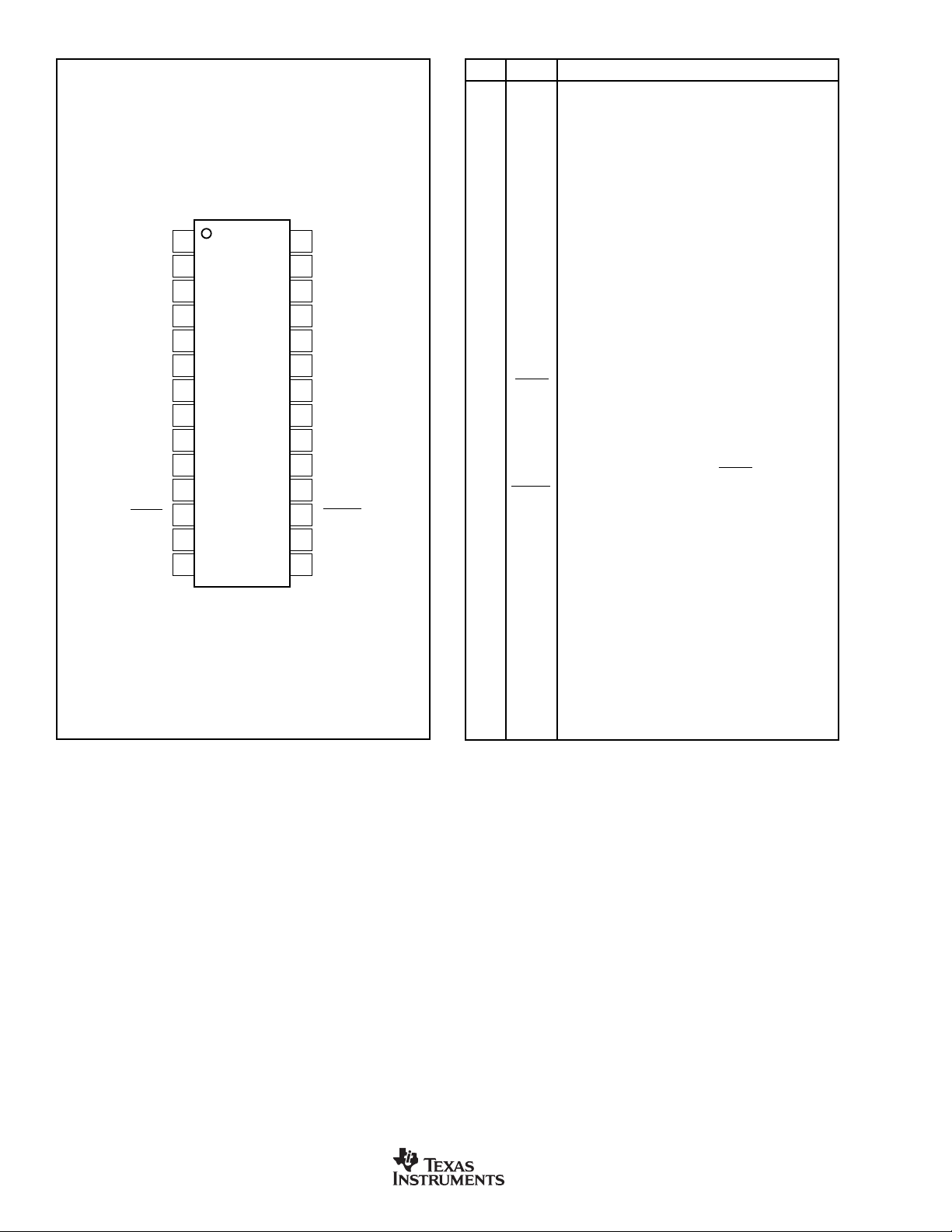
PIN CONFIGURATION
Top View SO
IN1
AGND
CAP1B
CAP1B
CAP1A
CAP1A
AV
TEST
CONV
CLK
DCLK
DXMIT
DIN
DV
1
2
3
4
5
6
7
DD
DD
DDC112U
8
9
10
11
12
13
14
28
IN2
27
AGND
26
CAP2B
25
CAP2B
24
CAP2A
23
CAP2A
22
V
REF
21
AGND
20
RANGE2 (MSB)
19
RANGE1
18
RANGE0 (LSB)
17
DVALID
16
DOUT
15
DGND
PIN DESCRIPTIONS
PIN LABEL DESCRIPTION
1 IN1 Input 1: analog input for Integrators 1A and 1B. The
2 AGND Analog Ground
3 CAP1B External Capacitor for Integrator 1B
4 CAP1B External Capacitor for Integrator 1B
5 CAP1A External Capacitor for Integrator 1A
6 CAP1A External Capacitor for Integrator 1A
7AV
8 TEST Test Control Input. When HIGH, a test charge is applied
9 CONV Controls which side of the integrator is connected to
10 CLK System Clock Input, 10MHz Nominal
11 DCLK Serial Data Clock Input. This input operates the serial I/
12 DXMIT Serial Data Transmit Enable Input. When LOW, this
13 DIN Serial Digital Input. Used to cascade multiple DDC112s.
14 DV
15 DGND Digital Ground
16 DOUT Serial Data Output, Hi-Z when DXMIT is HIGH
17 DVALID Data Valid Output. A LOW value indicates valid data is
18 RANGE0 Range Control Input 0 (least significant bit)
19 RANGE1 Range Control Input 1
20 RANGE2 Range Control Input 2 (most significant bit)
21 AGND Analog Ground
22 V
23 CAP2A External Capacitor for Integrator 2A
24 CAP2A External Capacitor for Integrator 2A
25 CAP2B External Capacitor for Integrator 2B
26 CAP2B External Capacitor for Integrator 2B
27 AGND Analog Ground
28 IN2 Input 2: analog input for Integrators 2A and 2B. The
integrator that is active is set by the CONV input.
Analog Supply, +5V Nominal
DD
to the A or B integrators on the next CONV transition.
input. In continuous mode; CONV HIGH → side A is
integrating, CONV LOW → side B is integrating. CONV
must be synchronized with CLK (see Figure 2).
O shift register.
input enables the internal serial shift register.
Digital Supply, +5V Nominal
DD
available in the serial I/O register.
External Reference Input, +4.096V Nominal
REF
integrator that is active is set by the CONV input.
4
www.ti.com
DDC112
SBAS085B
Page 5

DDC112
SBAS085B
5
Page 6

TYPICAL CHARACTERISTICS
At TA = +25°C, characterization done with Range 5 (250pC), T
= 500µs, V
INT
= +4.096, AVDD = DVDD = +5V, and CLK = 10MHz, unless otherwise noted.
REF
70
60
50
Range 0
40
(C
EXT
30
20
Noise (ppm of FSR, rms)
10
0
200 8000 1000600400
5
4.5
C
SENSOR
= 50pF
4
3.5
3
C
= 0pF
SENSOR
2.5
2
1.5
1
Noise (ppm of FSR, rms)
0.5
Range 5
0
30 4020 9010 10070 80 1050 60
NOISE vs C
SENSOR
Range 1
= 250pF)
Range 7
C
(pF)
SENSOR
NOISE vs INPUT LEVEL
Input Level (% of Full-Scale)
Range 2
6
5
C
= 50pF
SENSOR
4
C
= 0pF
SENSOR
NOISE vs T
INT
3
2
Noise (ppm of FSR, rms)
Range 5
1
0
1 10000.1 10010
T
(ms)
INT
NOISE vs TEMPERATURE
9
8
Range 1
7
6
5
4
3
2
Noise (ppm of FSR, rms)
C
= 0pF
SENSOR
1
Range 2
Range 3
Range 7
0
–40 –15 10 35 60 85
Temperature (°C)
2000
1500
1000
500
0
Range Drift (ppm)
–500
–1000
–1500
–40 –15 10 35 60 85
6
RANGE DRIFT vs TEMPERATURE
Ranges 1 - 7
(Internal Integration Capacitor)
Temperature (°C)
www.ti.com
IB vs TEMPERATURE
10
All Ranges
1
(pA)
B
I
0.1
0.01
25 35 45 55 65 75 85
Temperature (°C)
DDC112
SBAS085B
Page 7

DDC112
SBAS085B
7
Page 8
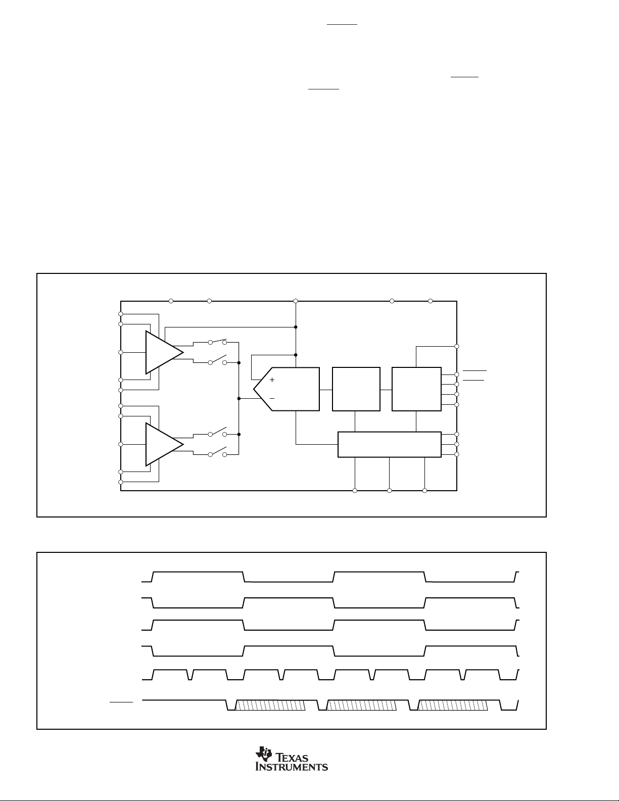
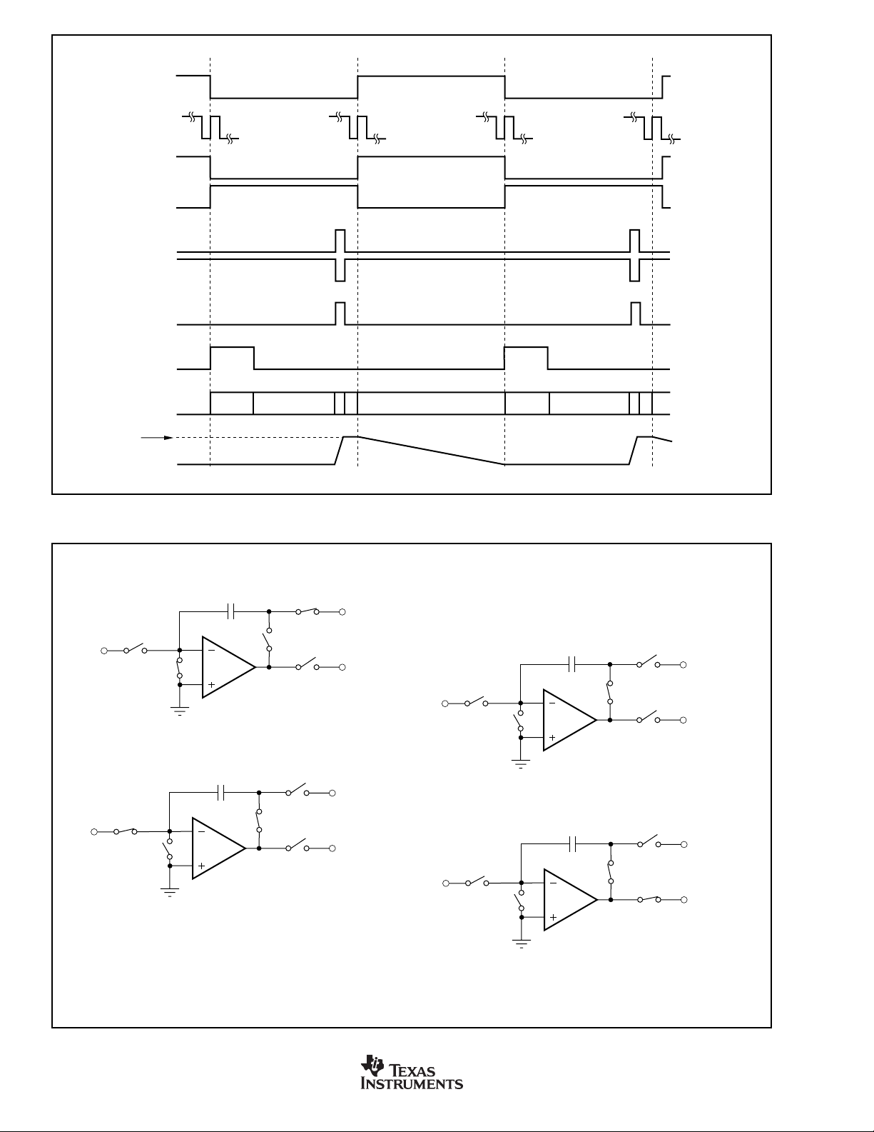
THEORY OF OPERATION
The basic operation of the DDC112 is illustrated in
The device contains two identical input channels where each
performs the function of current-to-voltage integration followed by a multiplexed analog-to-digital (A/D) conversion.
Each input has two integrators so that the current-to-voltage
integration can be continuous in time. The output of the four
integrators are switched to one delta-sigma (∆Σ) converter
via a four input multiplexer. With the DDC112 in the continuous integration mode, the output of the integrators from one
side of both of the inputs will be digitized while the other two
integrators are in the integration mode as illustrated in the
timing diagram in Figure 2. This integration and A/D conversion process is controlled by the system clock, CLK. With a
10MHz system clock, the integrator combined with the deltasigma converter accomplishes a single 20-bit conversion in
approximately 220µs. The results from side A and side B of
each signal input are stored in a serial output shift register.
Figure 1.
The DVALID
output goes LOW when the shift register
contains valid data.
The digital interface of the DDC112 provides the digital
results via a synchronous serial interface consisting of a data
clock (DCLK), a transmit enable pin (
(DVALID
), a serial data output pin (DOUT), and a serial data
DXMIT
), a valid data pin
input pin (DIN). The DDC112 contains only one A/D converter, so the conversion process is interleaved between the
two inputs, as shown in Figure 2. The integration and
conversion process is fundamentally independent of the data
retrieval process. Consequently, the CLK frequency and
DCLK frequencies need not be the same. DIN is only used
when multiple converters are cascaded and should be tied to
DGND otherwise. Depending on T
, CLK, and DCLK, it is
INT
possible to daisy-chain over 100 converters. This greatly
simplifies the interconnection and routing of the digital outputs in cases where a large number of converters are
needed.
CAP1A
CAP1A
IN1
CAP1B
CAP1B
CAP2A
CAP2A
IN2
CAP2B
CAP2B
FIGURE 1. Block Diagram.
IN1, Integrator A
DD
Input 1
Dual
Switched
Integrator
Input 2
Dual
Switched
Integrator
Integrate
AGNDAV
V
REF
∆Σ
Modulator
Digital
Filter
TEST
Control
CONV
Integrate
DD
Digital
Input/Output
CLK
DGNDDV
DCLK
DVALID
DXMIT
DOUT
DIN
RANGE2
RANGE1
RANGE0
IN1, Integrator B
IN2, Integrator A
IN2, Integrator B
Conversion in Progress
DVALID
Integrate
IN1B IN2B IN1A
Integrate
Integrate
Integrate
IN2A IN1B IN2B IN1A
FIGURE 2. Basic Integration and Conversion Timing for the DDC112 (continuous mode).
8
www.ti.com
Integrate
Integrate
IN2A
DDC112
SBAS085B
Page 9

DDC112
SBAS085B
9
Page 10
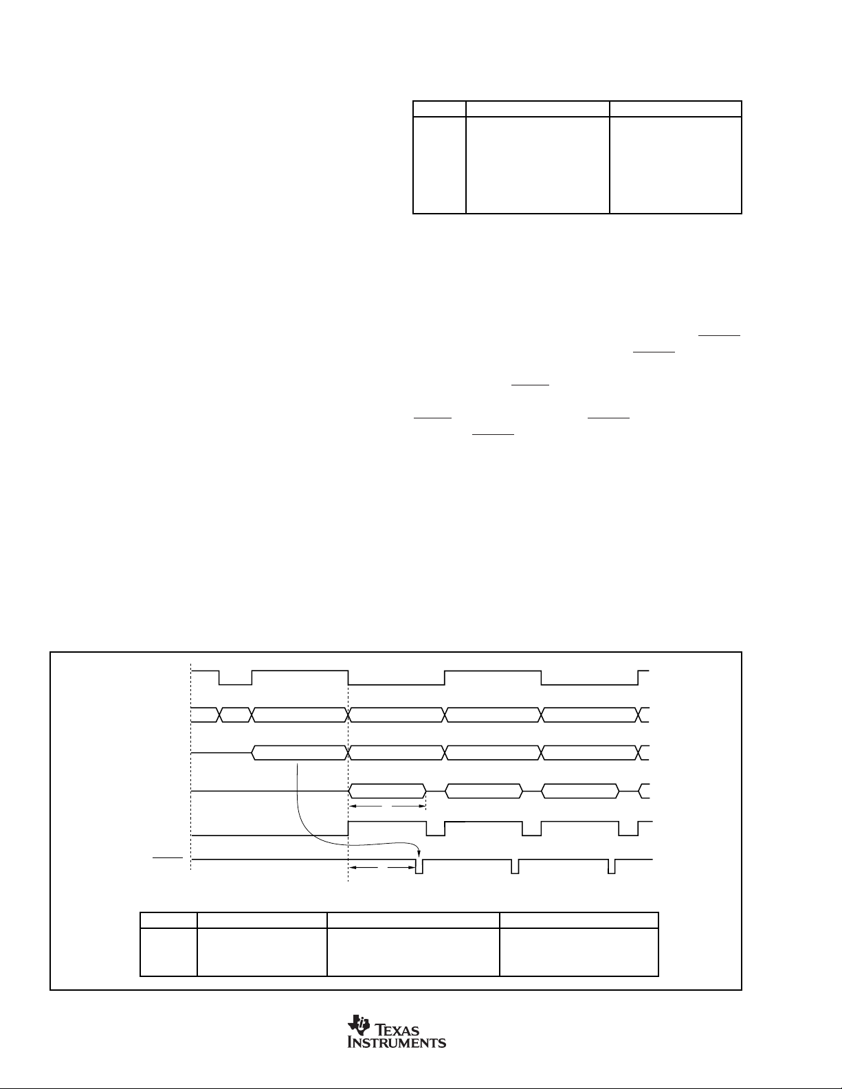
CONV
CLK
S
INTA
S
INTB
S
REF1
S
REF2
S
RESET
S
A/D1A
Configuration of
Integrator A
V
REF
WaitConvert WaitConvertIntegrate
Reset
Wait
Integrator A
Voltage Output
FIGURE 4. Basic Integrator Timing Diagram as Illustrated in Figure 3.
S
S
REF2
REF2
S
S
S
S
REF1
A/D
REF1
A/D
V
REF
To Converter
V
REF
To Converter
IN
IN
S
INT
IN
S
RESET
a) Reset Configuration
S
INT
IN
S
RESET
c) Integrate Configuration
C
F
C
F
S
INT
S
RESET
b) Wait Configuration
S
INT
S
RESET
Wait
Reset
S
S
REF1
REF2
V
REF
C
F
To Converter
S
A/D
S
REF2
S
REF1
V
REF
C
F
To Converter
S
A/D
d) Convert Configuration
FIGURE 5. Diagrams for the Four Configurations of the Front End Integrators of the DDC112.
10
www.ti.com
DDC112
SBAS085B
Page 11

DDC112
SBAS085B
11
Page 12

A low-pass filter to reduce noise connects it to an operational amplifier configured as a buffer. This amplifier should
have a unity-gain bandwidth greater than 4MHz, low noise,
and input/output common-mode ranges that support V
REF
Following the buffer are capacitors placed close to the
DDC112 V
pin. Even though the circuit in Figure 6 might
REF
appear to be unstable due to the large output capacitors, it
works well for most operational amplifiers. It is NOT recommended that series resistance be placed in the output lead
to improve stability since this can cause droop in V
REF
which
produces large offsets.
DDC112 Frequency Response
The frequency response of the DDC112 is set by the front end
integrators and is that of a traditional continuous time integrator, as shown in Figure 7. By adjusting T
, the user can
INT
change the 3dB bandwidth and the location of the notches in
the response. The frequency response of the ∆Σ converter that
follows the front end integrator is of no consequence because
the converter samples a held signal from the integrators. That
is, the input to the ∆Σ converter is always a DC signal. Since
the output of the front end integrators are sampled, aliasing can
occur. Whenever the frequency of the input signal exceeds
one-half of the sampling rate, the signal will
fold
back down to
lower frequencies.
Test Mode
When TEST is used, pins IN1 and IN2 are grounded and
packets
of approximately 13pC charge are transferred to the
0
.
–10
–20
–30
Gain (dB)
–40
–50
0.1
T
INT
1
T
INT
Frequency
10
T
INT
FIGURE 7. Frequency Response of the DDC112.
integration capacitors of both Input 1 and Input 2. This fixed
charge can be transferred to the integration capacitors either
once during an integration cycle or multiple times. In the case
where multiple packets are transferred during one integration
period, the 13pC charge is additive. This mode can be used
in both the continuous and noncontinuous mode timing. The
timing diagrams for test mode are shown in Figure 8. The top
three lines in Figure 8 define the timing when one packet of
13pC is sent to the integration capacitors. The bottom three
lines define the timing when multiple packets are sent to the
integration capacitors.
100
T
INT
Action
CONV
TEST
Action
CONV
TEST
Test Mode Disabled
Integrate B
Test Mode Disabled
Integrate B Integrate A
Integrate A
Test Mode Enabled
13pC into B 13pC into A 13pC into B 13pC into A
t
1
Test Mode Enabled
13pC into B 26pC into A 39pC into B 52pC into A
t
4
t
1
t
3
t
5
Test Mode Disabled
Integrate B Integrate A
t
2
Test Mode Disabled
Integrate B Integrate A
t
2
t
4
FIGURE 8. Timing Diagram of the Test Mode of the DDC112.
CLK = 10MHz CLK = 15MHz
SYMBOL DESCRIPTION MIN TYP MAX MIN TYP MAX UNITS
t
1
t
2
t
3
t
4
t
5
Setup Time for Test Mode Enable 100 100 ns
Setup Time for Test Mode Disable 100 100 ns
Hold Time for Test Mode Enable 100 100 ns
From Rising Edge of TEST to the Edge of CONV 5.4 3.6 µs
while Test Mode Enabled
Rising Edge to Rising Edge of TEST 5.4 3.6 µs
TABLE III. Timing for the DDC112 in the Test Mode.
12
www.ti.com
DDC112
SBAS085B
Page 13

DDC112
SBAS085B
13
Page 14
During the cont mode, mbsy is not active when CONV
toggles. The non-integrating side is always ready to begin
integrating when the other side finishes its integration. Consequently, keeping track of the current status of CONV is all
that is needed to know the current state. Cont mode operation corresponds to states 3-6. Two of the states, 3 and 6,
only perform an integration (no m/r/az cycle).
mbsy becomes important when operating in the ncont mode;
states 1, 2, 7, and 8. Whenever CONV is toggled while mbsy
is active, the DDC112 will enter or remain in either ncont
state 1 (or 8). After mbsy goes inactive, state 2 (or 7) is
entered. This state prepares the appropriate side for integration. As mentioned above, in the ncont states, the inputs to
the DDC112 are grounded.
One interesting observation from the state diagram is that the
integrations always alternate between sides A and B. This
relationship holds for any CONV pattern and is independent
of the mode. States 2 and 7 insure this relationship during the
ncont mode.
When power is first applied to the DDC112, the beginning
state is either 1 or 8, depending on the initial level of CONV.
For CONV held HIGH at power-up, the beginning state is 1.
Conversely, for CONV held LOW at power-up, the beginning
state is 8. In general, there is a symmetry in the state
diagram between states 1-8, 2-7, 3-6, and 4-5. Inverting
CONV results in the states progressing through their symmetrical match.
TIMING EXAMPLES
Cont Mode
A few timing diagrams will now be discussed to help illustrate
the operation of the state machine. These are shown in
Figures 10 through 19. Table V gives generalized timing
specifications in units of CLK periods. Values in µs for
Table V can be easily found for a given CLK. For example,
if CLK = 10MHz, then a CLK period = 0.1µs. t
in Table V
6
would then be 479.4µs.
SYMBOL DESCRIPTION VALUE (CLK periods)
Cont mode m/r/az cycle. 4794
t
6
t
Cont mode data ready. 4212 (t
7
t
1st ncont mode data ready. 4212 ±3
8
t
2nd ncont mode data ready. 4548
9
t
Ncont mode m/r/az cycle. 9108
10
4212 ±3(t
> 4794)
INT
= 4794)
INT
T ABLE V . Timing Specifications Generalized in CLK Periods.
Figure 10 shows a few integration cycles beginning with
initial power-up for a cont mode example. The top signal is
CONV and is supplied by the user. The next line indicates the
current state in the state diagram. The following two traces
show when integrations and measurement cycles are underway. The internal signal mbsy is shown next. Finally, DVALID
is given. As described in the data sheet, DVALID goes active
LOW when data is ready to be retrieved from the DDC112.
It stays LOW until
DXMIT
is taken LOW by the user. In Figure
10 and the following timing diagrams, it is assumed that
DXMIT
it taken LOW soon after DVALID goes LOW. The text
below the DVALID
pulse indicates the side of the data and
arrows help match the data to the corresponding integration.
The signals shown in Figures 10 through 19 are drawn at
approximately the same scale.
In Figure 10, the first state is ncont state 1. The DDC112
always powers up in the ncont mode. In this case, the first
state is 1 because CONV is initially HIGH. After the first two
states, cont mode operation is reached and the states begin
toggling between 4 and 5. From now on, the input is being
continuously integrated, either by side A or side B. The time
needed for the m/r/az cycle, t
, is the same time that
6
CONV
State
Integration
Status
m/r/az
Status
mbsy
DVALID
SYMBOL
t
6
t
7
t = 0
Power-Up
DESCRIPTION VALUE (CLK = 10MHz) VALUE (CLK = 15MHz)
Cont mode m/r/az cycle. 479.4µs 319.6µs
Cont mode data ready. 421.2µs(T
421.2 ±0.3µs(T
432154
Integrate BIntegrate A Integrate A Integrate B
m/r/az A m/r/az B m/r/az A
t
6
t
7
Side A
FIGURE 10. Continuous Mode Timing (CONV HIGH at power-up).
14
www.ti.com
Data
> 479.4µs) 280.8µs(T
INT
= 479.4µs) 280.8 ±0.2µs(T
INT
Side B
Data
Side A
Data
> 319.6µs)
INT
= 319.6µs)
INT
DDC112
SBAS085B
Page 15

DDC112
SBAS085B
15
Page 16

Ncont Mode
Figure 13 illustrates operation in the ncont mode. The
integrations come in pairs (that is, sides A/B or sides B/A)
followed by a time during which no integrations occur.
During that time, the previous integrations are being measured, reset and auto-zeroed. Before the DDC112 can
advance to states 3 or 6, both sides A and B must be
finished with the m/r/az cycle which takes time t
m/r/az cycles are completed, time t
is needed to prepare
11
the next side for integration. This time is required for the
ncont mode because the m/r/az cycle of the ncont mode is
slightly different from that of the cont mode. After the first
integration ends, DVALID
CONV
goes LOW in time t8. This is the
. When the
10
same time as in the cont mode. The second data will be
ready in time t
after the first data is ready. One result of the
9
naming convention used in this application bulletin is that
when the DDC112 is operating in the
through both
ncont mode states
ncont mode
and
cont mode states
, it passes
. For
example, in Figure 13, the state pattern is 3, 4, 1, 2, 3, 4, 1,
2, 3, 4...where 3 and 4 are cont mode states.
Ncont mode
by definition means that for some portion of the time, neither
side A nor B is integrating. States that perform an integration
are labeled
called
cont mode states
ncont mode states
while those that do not are
. Since integrations are performed
in the ncont mode, just not continuously, some cont mode
states must be used in an ncont mode state pattern.
State
Integration
Status
m/r/az
Status
mbsy
DVALID
SYMBOL
t
8
t
9
t
10
t
11
23134 4 1 2
t
11
Int BInt AInt BInt A
m/r/az Bm/r/az A
t
10
t
9
t
8
Side A
Data
DESCRIPTION VALUE (CLK = 10MHz) VALUE (CLK = 15MHz)
1st ncont mode data ready. 421.2 ±0.3µs 280.8 ±0.2µs
2nd ncont mode data ready. 454.8µs 303.2µs
Ncont mode m/r/az cycle. 910.8µs 607.2µs
Prepare side for integration. ≥ 24.0µs ≥ 24.0µs
Side B
Data
m/r/az A m/r/az B
Side A
Data
Side B
Data
FIGURE 13. Non-Continuous Mode Timing.
16
www.ti.com
DDC112
SBAS085B
Page 17

DDC112
SBAS085B
17
Page 18

Looking at the state diagram, one can see that the CONV
pattern needed to generate a given state progression is not
unique. Upon entering states 1 or 8, the DDC112 remains in
those states until mbsy goes LOW, independent of CONV.
As long as the m/r/az cycle is underway, the state machine
ignores CONV (see Figure 9). The top two signals are
different CONV patterns that produce the same state.
This feature can be a little confusing at first, but it does allow
flexibility in generating ncont mode CONV patterns. For
example, the DDC112 Evaluation Fixture operates in the
ncont mode by generating a square wave with pulse width
< t
. Figure 17 illustrates operation in the ncont mode using
6
CONV1
CONV2
mbsy
a 50% duty cycle CONV signal with T
= 1620 CLK
INT
periods. Care must be exercised when using a square wave
to generate CONV. There are certain integration
times that
must be avoided since they produce very short intervals for
state 2 (or state 7 if CONV is inverted). As seen in the state
diagram, the state progresses from 2 to 3 as soon as CONV
is HIGH. The state machine does not insure that the duration
of state 2 is long enough to properly prepare the next side
for integration (t
). This must be done by the user with
11
proper timing of CONV. For example, if CONV is a square
wave with T
CLK periods long, therefore, t
= 3042 CLK periods, state 2 will only be 18
INT
will not be met.
11
State
FIGURE 16. Equivalent CONV Signals in Non-Continuous Mode.
CONV
State
Integration
Status
mbsy
DVALID
Int A
Side A
Data
23134 4 1 2
23134 41
Int BInt AInt B
Side B
Data
Side A
Data
FIGURE 17. Non-Continuous Mode Timing with a 50% Duty Cycle CONV Signal.
18
www.ti.com
DDC112
SBAS085B
Page 19

DDC112
SBAS085B
19
Page 20

SPECIAL CONSIDERATIONS
NCONT MODE INTEGRATION TIME
The DDC112 uses a relatively fast clock. For CLK = 10MHz,
this allows T
should be synchronized to CLK. However, for the internal
measurement, reset and auto-zero operations, a slower
clock is more efficient. The DDC112 divides CLK by six and
uses this slower clock with a period of 600ns to run the m/r/
az cycle and data ready logic.
Because of the divider, it is possible for the integration time
to be a non-integer number of slow clock periods.
example, if T
there will be 833 1/3 slow clocks in an integration period. This
non-integer relationship between T
period causes the number of rising and falling slow clock
edges within an integration period to change from integration
to integration. The digital coupling of these edges to the
integrators will in turn change from integration to integration
which produces noise. The change in the clock edges is not
random, but will repeat every 3 integrations. The coupling
noise on the integrators appears as a tone with a frequency
equal to the rate at which the coupling repeats.
To avoid this problem in cont mode, the internal slow clock
is shut down after the m/r/az cycle is complete when it is no
longer needed. It starts up again just after the next integration begins. Since the slow clock is always off when CONV
toggles, the same number of slow clock edges fall within an
integration period regardless of its length. Therefore,
T
≥ 4794 CLK periods will not produce the coupling
INT
problem described above.
For the ncont mode however, the slow clock must always be
left running. The m/r/az cycle is not completed before an
integration ends. It is then possible to have digital coupling to
the integrators. The digital coupling noise depends heavily on
the layout of the printed circuit board used for the DDC112.
For solid grounds and power supplies with good bypassing,
it is possible to greatly reduce the coupling. However, for
ensuring the best performance in the ncont mode, the integration time should be chosen to be an integer multiple of
1/(2f
SLOWCLOCK
should be an integer multiple of 300ns—T
A better choice would be T
DATA READY
The DVALID signal which indicates that data is ready is
generated using the internal slow clock. The phase relationship between this clock and CLK is set when power is first
applied and is random. Since CONV is synchronized with
CLK, it will have a random phase relationship with respect to
the slow clock. When T
shut down as described above. This shutdown process
synchronizes the internal clock with CONV so that the time
between when CONV toggles to when
(t
and t8) is fixed.
7
to be adjusted in steps of 100ns since CONV
INT
= 5000 CLK periods (500µs for CLK = 10MHz),
INT
and the slow clock
INT
). For CLK = 10MHz, the integration time
= 100µs is not.
= 99µs.
INT
> t6, the slow clock will temporarily
INT
INT
DVALID
goes LOW
For
For T
≤ t6, the internal slow clock, is not allowed to shut
INT
down and the synchronization never occurs. Therefore, the
time between CONV toggling and DVALID
indicating data is
ready has uncertainty due to the random phase relationship
between CONV and the slow clock. This variation is
±1/(2f
SLOWCLOCK
) or ±3/f
. The timing to the second DVALID
CLK
in the ncont mode will not have a variation since it is
triggered off the first data ready (t
) and both are derived
9
from the slow clock.
Polling DVALID
to determine when data is ready eliminates
any concern about the variation in timing since the readback
is automatically adjusted as needed. If the data readback is
triggered off the toggling of CONV directly (instead of polling), then waiting the maximum value of t
or t8 insures that
7
data will always be ready before readback occurs.
Data Retrieval
In the continuous and noncontinuous modes of operation,
the data from the last conversion is available for retrieval with
the falling edge of DVALID
of
DXMIT
in combination with the data clock (DCLK) will
(see Figure 22). The falling edge
initiate the serial transmission of the data from the DDC112.
Typically, data is retrieved from the DDC112 as soon as
DVALID
falls and completed before the next CONV transition
from HIGH to LOW or LOW to HIGH occurs. If this is not the
case, care should be taken to stop activity on DCLK and
consequently DOUT by at least 10µs around a CONV transition. If this caution is ignored it is possible that the integration that is being initiated by CONV will have additional noise
introduced.
The serial output data at DOUT is transmitted in Straight
Binary Code per Table VIII. An output offset has been built
into the DDC112 to allow for the measurement of input
signals near and below zero. Board leakage up to
≈ –0.4%
of the positive full-scale can be tolerated before the digital
output clips to all zeroes.
CODE INPUT SIGNAL
1111 1111 1111 1111 1111 FS
1111 1111 1111 1111 1110 FS – 1LSB
0000 0001 0000 0000 0001 +1LSB
0000 0001 0000 0000 0000 Zero
0000 0000 0000 0000 0000 –0.4% FS
TABLE VIII. Straight Binary Code Table.
Cascading Multiple Converters
Multiple DDC112 units can be connected in serial or parallel
configurations, as illustrated in Figures 20 and 21.
DOUT can be used with DIN to
devices together to minimize wiring. In this mode of operation, the serial data output is shifted through multiple DDC112s,
as illustrated in Figure 20.
R
prevents DIN from floating when
PULLUP
Care should be taken to keep the capacitive load on DOUT
as low as possible when running CLK=15MHz.
daisy-chain
several DDC112
DXMIT
is HIGH.
20
www.ti.com
DDC112
SBAS085B
Page 21

DDC112
SBAS085B
21
Page 22

CLK
DVALID
DXMIT
DCLK
t
18
t
14
t
20
(1)
t
26
t
22
DIN
t
21
DOUT
NOTE: (1) Disable DCLK (preferably LOW) when DXMIT is HIGH.
Output Disabled
Output Disabled
Input A
Bit 1
MSB
Output Enabled
Output Enabled
t
22A, t22B
t
24
Input E
Bit 20
Input F
LSB LSB Output DisabledMSB
Bit 1
t
25
Input F
Bit 20
t
23
Output Disabled
FIGURE 23. Timing Diagram When Using the DIN Function of the DDC112.
CLK = 10MHz CLK = 15MHz
SYMBOL DESCRIPTION MIN TYP MAX MIN TYP MAX UNITS
t
24
t
25
t
26
Set-Up Time From DIN to Rising Edge of DCLK 10 5 ns
Hold Time For DIN After Rising Edge of DCLK 10 10 ns
Hold Time for DXMIT HIGH Before Falling 2 1.33 µs
Edge of DVALID
TABLE X. Timing for the DDC112 Data Retrieval Using DIN.
RETRIEVAL
(CONTINUOUS MODE)
This is the most straightforward method. Data retrieval begins soon after DVALID
CONV toggles, see Figure 24. For best performance, data
retrieval must stop t
the most appropriate for longer integration times. The maximum time available for readback is T
For DCLK and CLK = 10MHz, the maximum number of
DDC112s that can be daisy-chained together is:
Where τ
T
= 1000µs and DCLK = 10MHz, the maximum number of
INT
BEFORE
CONV TOGGLES
goes LOW and finishes before
before CONV toggles. This method is
28
– t27 – t28.
INT
Ts
– .431 240µ
INT
τ
DCLK
is the period of the data clock. For example, if
DCLK
RETRIEVAL
AFTER
CONV TOGGLES
(CONTINUOUS MODE)
For shorter integration times, more time is available if data
retrieval begins after CONV toggles and ends before the new
data is ready. Data retrieval must wait t
before beginning. Figure 25 shows an example of this. The
maximum time available for retrieval is t
(421.2µs – 10µs – 2µs for CLK = 10MHz), regardless of T
The maximum number of DDC112s that can be daisychained together is:
409 240. µs
τ
DCLK
For DCLK = 10MHz, the maximum number of DDC112s is
102.
after CONV toggles
29
– t29 – t
27
DDC112s is:
INT
26
.
22
1000 431 2
µµ
ss
– .
40 100
()( )
ns
142 2 142 112
=→
.
DDC s
www.ti.com
DDC112
SBAS085B
Page 23

DDC112
SBAS085B
23
Page 24

RETRIEVAL
BEFORE
AND
AFTER
CONV
TOGGLES (CONTINUOUS MODE)
For the absolute maximum time for data retrieval, data can
be retrieved
before and after
CONV toggles. Nearly all of T
INT
is available for data retrieval. Figure 26 illustrates how this is
done by combining the two previous methods. You must
pause the retrieval during CONV toggling to prevent digital
noise, as discussed previously, and finish before the next
data is ready. The maximum number of DDC112s that can
be daisy-chained together is:
Tss
––20 2
µµ
INT
40
τ
DCLK
For T
= 500µs and DCLK = 10MHz, the maximum number
INT
of DDC112s is 119.
RETRIEVAL: NONCONTINUOUS MODE
Retrieving in noncontinuous mode is slightly different as
compared with the continuous mode. As shown in Figure 27
and described in detail in Application Bulletin SBAA024
(available for download at www.ti.com), DVALID
in time t
shorter than this time, all of t
after the first integration completes. If T
30
is available to retrieve data
31
before the other side’s data is ready. For T
goes LOW
> t30, the first
INT
INT
is
integration’s data is ready before the second integration
completes. Data retrieval must be delayed until the second
integration completes leaving less time available for retrieval.
The time available is t
31
– (T
– t30). The second integration’s
INT
data must be retrieved before the next round of integrations
begin. This time is highly dependent on the pattern used to
generate CONV. As with the continuous mode, data retrieval
must halt before and after CONV toggles (t
completed before new data is ready (t
and t29) and be
28
).
26
POWER-UP SEQUENCING
Prior to power-up, all digital and analog input pins must be
LOW. At the time of power-up, these signal inputs can be
biased to a voltage other than 0V, however, they should
never exceed AV
up is used to determine which side (A or B) will be integrated
first. Before integrations can begin though, CONV must
toggle; see Figure 28.
or DVDD. The level of CONV at power-
DD
CONV
DVALID
DXMIT
DCLK
DOUT
SYMBOL DESCRIPTION MIN TYP MAX MIN TYP MAX UNITS
t
26
t
28
t
29
••• ••• ••• ••• ••• •••
••• ••• •••
Hold Time for DXMIT HIGH Before Falling 2 1.33 µs
Data Retrieval Shutdown Before Edge of CONV 10 10 µs
Data Retrieval Start-Up After dge of CONV 10 10 µs
T
INT
Edge of DVALID
T
INT
t
29
t
28
Side B
Data
t
26
••• ••• •••
Side A
Data
CLK = 10MHz CLK = 15MHz
T
INT
FIGURE 26. Readback
24
Before and After
CONV Toggles.
www.ti.com
DDC112
SBAS085B
Page 25

DDC112
SBAS085B
25
Page 26
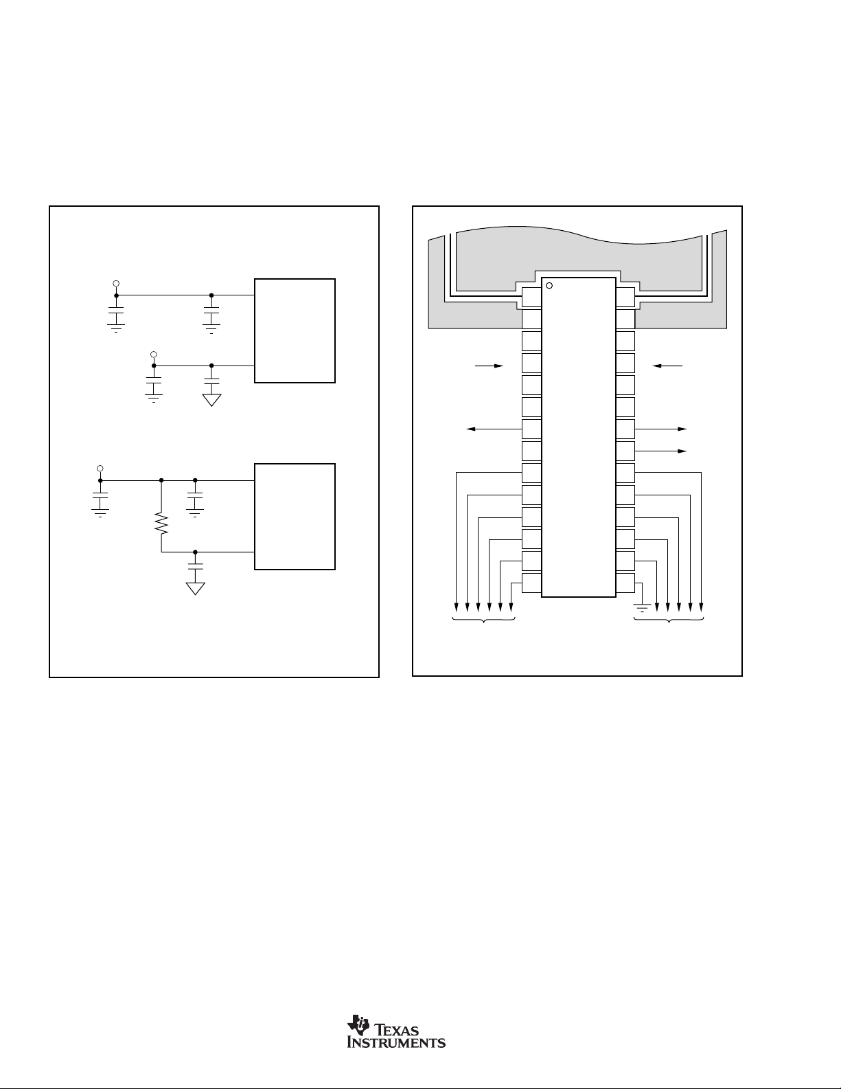
Input shielding practices should be taken into consideration
when designing the circuit layout for the DDC112. The inputs
to the DDC112 are high impedance and extremely sensitive
to extraneous noise. Leakage currents between the PCB
traces can exceed the input bias current of the DDC112 if
shielding is not implemented. Figure 30 illustrates an acceptable approach to this problem. A PC ground plane is placed
around the inputs of the DDC112. This shield helps minimize
coupled noise into the input pins. Additionally, the pins that
V
+
S
AV
DV
AV
DV
DD
DDC112
DD
DD
DDC112
DD
10µF
+
V
DD
10µF
V
+
S
10µF
< 10Ω
0.1µF
0.1µF
Separate +5V Supplies
0.1µF
0.1µF
are used for the external integration capacitors should be
guarded by a ground plane when the external capacitors are
used.
The approach above reduces leakage affects by surrounding
these sensitive pins with a low impedance analog ground.
Leakage currents from other portions of the circuit will flow
harmlessly to the low impedance analog ground rather than
into the analog input stage of the DDC112.
IN1 IN2
Analog
Ground
Analog
Ground
Shield
external
caps when
used
Analog
Power
1
2
3
4
5
6
7
8
9
10
11
12
13
14
DDC112U
28
27
26
25
24
23
22
21
20
19
18
17
16
15
Analog
Ground
Shield
external
caps when
used
Analog
Ground
One +5V Supply
FIGURE 29. Power Supply Connection Options.
Digital I/O
and
Digital Power
Digital I/O
and
Digital Power
FIGURE 30. Recommended Shield for DDC112U Layout
Design.
26
www.ti.com
DDC112
SBAS085B
Page 27

PACKAGE OPTION ADDENDUM
www.ti.com
5-Oct-2007
PACKAGING INFORMATION
Orderable Device Status
(1)
Package
Type
Package
Drawing
Pins Package
Qty
Eco Plan
DDC112U ACTIVE SOIC DW 28 20 Green (RoHS &
no Sb/Br)
DDC112U/1K ACTIVE SOIC DW 28 1000 Green (RoHS &
no Sb/Br)
DDC112U/1KG4 ACTIVE SOIC DW 28 1000 Green (RoHS &
no Sb/Br)
DDC112UG4 ACTIVE SOIC DW 28 20 Green (RoHS &
no Sb/Br)
DDC112UK ACTIVE SOIC DW 28 20 Green (RoHS &
no Sb/Br)
DDC112UK/1K ACTIVE SOIC DW 28 1000 Green (RoHS &
no Sb/Br)
DDC112UK/1KG4 ACTIVE SOIC DW 28 1000 Green (RoHS &
no Sb/Br)
DDC112UKG4 ACTIVE SOIC DW 28 20 Green (RoHS &
no Sb/Br)
DDC112Y/250 ACTIVE TQFP PJT 32 250 Green (RoHS &
no Sb/Br)
DDC112Y/250G4 ACTIVE TQFP PJT 32 250 Green (RoHS &
no Sb/Br)
DDC112Y/2K ACTIVE TQFP PJT 32 2000 Green (RoHS &
no Sb/Br)
DDC112Y/2KG4 ACTIVE TQFP PJT 32 2000 Green (RoHS &
no Sb/Br)
DDC112YK/250 ACTIVE TQFP PJT 32 250 Green (RoHS &
no Sb/Br)
DDC112YK/250G4 ACTIVE TQFP PJT 32 250 Green (RoHS&
no Sb/Br)
DDC112YK/2K ACTIVE TQFP PJT 32 2000 Green (RoHS &
no Sb/Br)
DDC112YK/2KG4 ACTIVE TQFP PJT 32 2000 Green (RoHS &
no Sb/Br)
(1)
The marketing status values are defined asfollows:
ACTIVE: Product device recommended for new designs.
LIFEBUY: TI has announced that the devicewill be discontinued, and alifetime-buy period is in effect.
NRND: Not recommended for new designs. Device is in production to support existing customers, but TI does not recommend using this part in
a new design.
PREVIEW: Device has been announced but isnot in production. Samples mayor may not be available.
OBSOLETE: TI has discontinued the production ofthe device.
(2)
Lead/Ball Finish MSL Peak Temp
CU NIPDAU Level-1-260C-UNLIM
CU NIPDAU Level-1-260C-UNLIM
CU NIPDAU Level-1-260C-UNLIM
CU NIPDAU Level-1-260C-UNLIM
CU NIPDAU Level-1-260C-UNLIM
CU NIPDAU Level-1-260C-UNLIM
CU NIPDAU Level-1-260C-UNLIM
CU NIPDAU Level-1-260C-UNLIM
CU NIPDAU Level-2-260C-1 YEAR
CU NIPDAU Level-2-260C-1 YEAR
CU NIPDAU Level-2-260C-1 YEAR
CU NIPDAU Level-2-260C-1 YEAR
CU NIPDAU Level-2-260C-1 YEAR
CU NIPDAU Level-2-260C-1 YEAR
CU NIPDAU Level-2-260C-1 YEAR
CU NIPDAU Level-2-260C-1 YEAR
(3)
(2)
Eco Plan - The planned eco-friendly classification: Pb-Free (RoHS), Pb-Free (RoHS Exempt), or Green (RoHS & no Sb/Br) - please check
http://www.ti.com/productcontent for the latest availability information andadditional product content details.
TBD: The Pb-Free/Green conversion plan has notbeen defined.
Pb-Free (RoHS): TI's terms "Lead-Free" or "Pb-Free" mean semiconductor products that are compatible with the current RoHS requirements
for all 6 substances, including the requirement that lead not exceed 0.1% by weight in homogeneous materials. Where designed to be soldered
at high temperatures, TI Pb-Free products aresuitable for use in specifiedlead-free processes.
Pb-Free (RoHS Exempt): This component has a RoHS exemption for either 1) lead-based flip-chip solder bumps used between the die and
package, or 2) lead-based die adhesive used between the die and leadframe. The component is otherwise considered Pb-Free (RoHS
compatible) as defined above.
Green (RoHS & no Sb/Br): TI defines "Green" to mean Pb-Free (RoHS compatible), and free of Bromine (Br) and Antimony (Sb) based flame
retardants (Br or Sb do not exceed0.1% by weight in homogeneousmaterial)
Addendum-Page 1
Page 28

PACKAGE OPTION ADDENDUM
www.ti.com
(3)
MSL, Peak Temp. -- The Moisture Sensitivity Level rating according to the JEDEC industry standard classifications, and peak solder
temperature.
Important Information and Disclaimer:The information provided on this page represents TI's knowledge and belief as of the date that it is
provided. TI bases its knowledge and belief on information provided by third parties, and makes no representation or warranty as to the
accuracy of such information. Efforts are underway to better integrate information from third parties. TI has taken and continues to take
reasonable steps to provide representative and accurate information but may not have conducted destructive testing or chemical analysis on
incoming materials and chemicals. TI and TI suppliers consider certain information to be proprietary, and thus CAS numbers and other limited
information may not be available for release.
In no event shall TI's liability arising out of such information exceed the total purchase price of the TI part(s) at issue in this document sold by TI
to Customer on an annual basis.
5-Oct-2007
Addendum-Page 2
Page 29
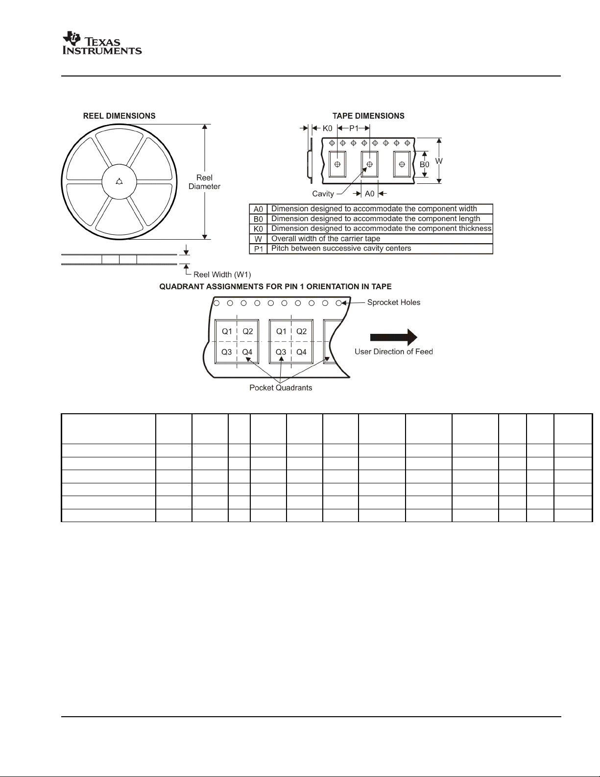
PACKAGE MATERIALS INFORMATION
www.ti.com
TAPE AND REEL INFORMATION
11-Mar-2008
*All dimensions are nominal
Device Package
Type
DDC112U/1K SOIC DW 28 1000 330.0 32.4 11.35 18.67 3.1 16.0 32.0 Q1
DDC112UK/1K SOIC DW 28 1000 330.0 32.4 11.35 18.67 3.1 16.0 32.0 Q1
DDC112Y/250 TQFP PJT 32 250 330.0 16.4 9.6 9.6 1.5 12.0 16.0 Q2
DDC112Y/2K TQFP PJT 32 2000 330.0 16.4 9.6 9.6 1.5 12.0 16.0 Q2
DDC112YK/250 TQFP PJT 32 250 330.0 16.4 9.6 9.6 1.5 12.0 16.0 Q2
DDC112YK/2K TQFP PJT 32 2000 330.0 16.4 9.6 9.6 1.5 12.0 16.0 Q2
Package
Drawing
Pins SPQ Reel
Diameter
(mm)
Reel
Width
W1 (mm)
A0 (mm) B0 (mm) K0 (mm) P1
(mm)W(mm)
Pin1
Quadrant
Pack Materials-Page 1
Page 30

PACKAGE MATERIALS INFORMATION
www.ti.com
11-Mar-2008
*All dimensions are nominal
Device Package Type Package Drawing Pins SPQ Length (mm) Width (mm) Height (mm)
DDC112U/1K SOIC DW 28 1000 346.0 346.0 49.0
DDC112UK/1K SOIC DW 28 1000 346.0 346.0 49.0
DDC112Y/250 TQFP PJT 32 250 346.0 346.0 33.0
DDC112Y/2K TQFP PJT 32 2000 346.0 346.0 33.0
DDC112YK/250 TQFP PJT 32 250 346.0 346.0 33.0
DDC112YK/2K TQFP PJT 32 2000 346.0 346.0 33.0
Pack Materials-Page 2
Page 31

MECHANICAL DATA
MPQF112 – NOVEMBER 2001
1
Page 32

Page 33

IMPORTANT NOTICE
Texas Instruments Incorporated and its subsidiaries (TI) reserve the right to make corrections, modifications, enhancements, improvements,
and other changes to its products and services at any time and to discontinue any product or service without notice. Customers should
obtain the latest relevant information before placing orders and should verify that such information is current and complete. All products are
sold subject to TI’s terms and conditions of sale supplied at the time of order acknowledgment.
TI warrants performance of its hardware products to the specifications applicable at the time of sale in accordance with TI’s standard
warranty. Testing and other quality control techniques are used to the extent TI deems necessary to support this warranty. Except where
mandated by government requirements, testing of all parameters of each product is not necessarily performed.
TI assumes no liability for applications assistance or customer product design. Customers are responsible for their products and
applications using TI components. To minimize the risks associated with customer products and applications, customers should provide
adequate design and operating safeguards.
TI does not warrant or represent that any license, either express or implied, is granted under any TI patent right, copyright, mask work right,
or other TI intellectual property right relating to any combination, machine, or process in which TI products or services are used. Information
published by TI regarding third-party products or services does not constitute a license from TI to use such products or services or a
warranty or endorsement thereof. Use of such information may require a license from a third party under the patents or other intellectual
property of the third party, or a license from TI under the patents or other intellectual property of TI.
Reproduction of TI information in TI data books or data sheets is permissible only if reproduction is without alteration and is accompanied
by all associated warranties, conditions, limitations, and notices. Reproduction of this information with alteration is an unfair and deceptive
business practice. TI is not responsible or liable for such altered documentation. Information of third parties may be subject to additional
restrictions.
Resale of TI products or services with statements different from or beyond the parameters stated by TI for that product or service voids all
express and any implied warranties for the associated TI product or service and is an unfair and deceptive business practice. TI is not
responsible or liable for any such statements.
TI products are not authorized for use in safety-critical applications (such as life support) where a failure of the TI product would reasonably
be expected to cause severe personal injury or death, unless officers of the parties have executed an agreement specifically governing
such use. Buyers represent that they have all necessary expertise in the safety and regulatory ramifications of their applications, and
acknowledge and agree that they are solely responsible for all legal, regulatory and safety-related requirements concerning their products
and any use of TI products in such safety-critical applications, notwithstanding any applications-related information or support that may be
provided by TI. Further, Buyers must fully indemnify TI and its representatives against any damages arising out of the use of TI products in
such safety-critical applications.
TI products are neither designed nor intended for use in military/aerospace applications or environments unless the TI products are
specifically designated by TI as military-grade or "enhanced plastic." Only products designated by TI as military-grade meet military
specifications. Buyers acknowledge and agree that any such use of TI products which TI has not designated as military-grade is solely at
the Buyer's risk, and that they are solely responsible for compliance with all legal and regulatory requirements in connection with such use.
TI products are neither designed nor intended for use in automotive applications or environments unless the specific TI products are
designated by TI as compliant with ISO/TS 16949 requirements. Buyers acknowledge and agree that, if they use any non-designated
products in automotive applications, TI will not be responsible for any failure to meet such requirements.
Following are URLs where you can obtain information on other Texas Instruments products and application solutions:
Products Applications
Amplifiers amplifier.ti.com Audio www.ti.com/audio
Data Converters dataconverter.ti.com Automotive www.ti.com/automotive
DSP dsp.ti.com Broadband www.ti.com/broadband
Clocks and Timers www.ti.com/clocks Digital Control www.ti.com/digitalcontrol
Interface interface.ti.com Medical www.ti.com/medical
Logic logic.ti.com Military www.ti.com/military
Power Mgmt power.ti.com Optical Networking www.ti.com/opticalnetwork
Microcontrollers microcontroller.ti.com Security www.ti.com/security
RFID www.ti-rfid.com Telephony www.ti.com/telephony
RF/IF and ZigBee® Solutions www.ti.com/lprf Video & Imaging www.ti.com/video
Mailing Address: Texas Instruments, Post Office Box 655303, Dallas, Texas 75265
Copyright © 2008, Texas Instruments Incorporated
Wireless www.ti.com/wireless
 Loading...