

Page 1
®
For most current data sheet and other product
information, visit www.burr-brown.com
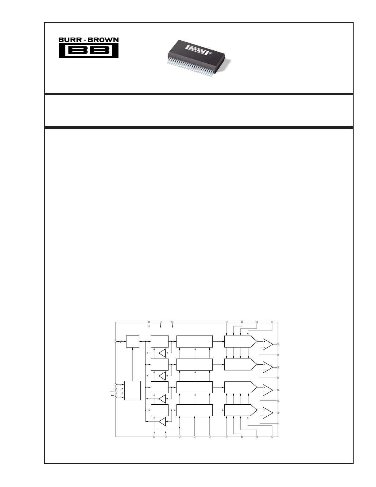
16-Bit, Quad Voltage Output
DIGITAL-TO-ANALOG CONVERTER
DAC7744
DAC7744
FEATURES
● LOW POWER: 200mW
● UNIPOLAR OR BIPOLAR OPERATION
● SINGLE-SUPPLY OUTPUT RANGE: +10V
● DUAL SUPPLY OUTPUT RANGE: ±10V
● SETTLING TIME: 10µs to 0.003%
● 16-BIT MONOTONICITY: –40°C to +85°C
● PROGRAMMABLE RESET TO MID-SCALE
OR ZERO-SCALE
● DATA READBACK
● DOUBLE-BUFFERED DATA INPUTS
APPLICATIONS
● PROCESS CONTROL
● ATE PIN ELECTRONICS
● CLOSED-LOOP SERVO-CONTROL
● MOTOR CONTROL
● DATA ACQUISITION SYSTEMS
● DAC-PER-PIN PROGRAMMERS
V
V
DAC7744
V
DD
CC
SS
DESCRIPTION
The DAC7744 is a 16-bit, quad voltage output digitalto-analog converter with guaranteed 16-bit monotonic
performance over the specified temperature range. It
accepts 16-bit parallel input data, has double-buffered
DAC input logic (allowing simultaneous update of all
DACs), and provides a readback mode of the internal
input registers. Programmable asynchronous reset
clears all registers to a mid-scale code of 8000H or to
a zero-scale of 0000H. The DAC7744 operates from
either a single +15V supply or from a +15V, –15V,
and +5V supply.
Low power and small size per DAC make the DAC7744
ideal for automatic test equipment, DAC-per-pin programmers, data acquisition systems, and closed-loop
servo-control. The DAC7744 is available in a 48lead SSOP package, and offers guaranteed specifications over the –40°C to +85°C temperature range.
V
V
REF
AB Sense
L
V
L AB V
REF
REF
H AB
REF
AB Sense
H
SBAS120
16
DATA I/O
A1
A0
CS
R/W
International Airport Industrial Park • Mailing Address: PO Box 11400, Tucson, AZ 85734 • Street Address: 6730 S. Tucson Blvd., Tucson, AZ 85706 • Tel: (520) 746-1111
Twx: 910-952-1111 • Internet: http://www.burr-brown.com/ • Cable: BBRCORP • Telex: 066-6491 • FAX: (520) 889-1510 • Immediate Product Info: (800) 548-6132
I/O
Buffer
Control
Logic
Input
Register A
Input
Register B
Input
Register C
Input
Register D
AGND DGND
© 1999 Burr-Brown Corporation PDS-1534A Printed in U.S.A. November, 1999
DAC
Register A
DAC
Register B
DAC
Register C
DAC
Register D
RST LOADDACs
RSTSEL
1
V
REF
CD Sense
DAC A
DAC B
DAC C
DAC D
V
L CD V
L
REF
H CD
REF
V
H
REF
CD Sense
V
V
V
V
V
V
V
V
OUT
OUTA
OUT
OUTB
OUT
OUTC
OUT
OUTD
A
Sense
B
Sense
C
Sense
D
Sense
DAC7744
®
Page 2
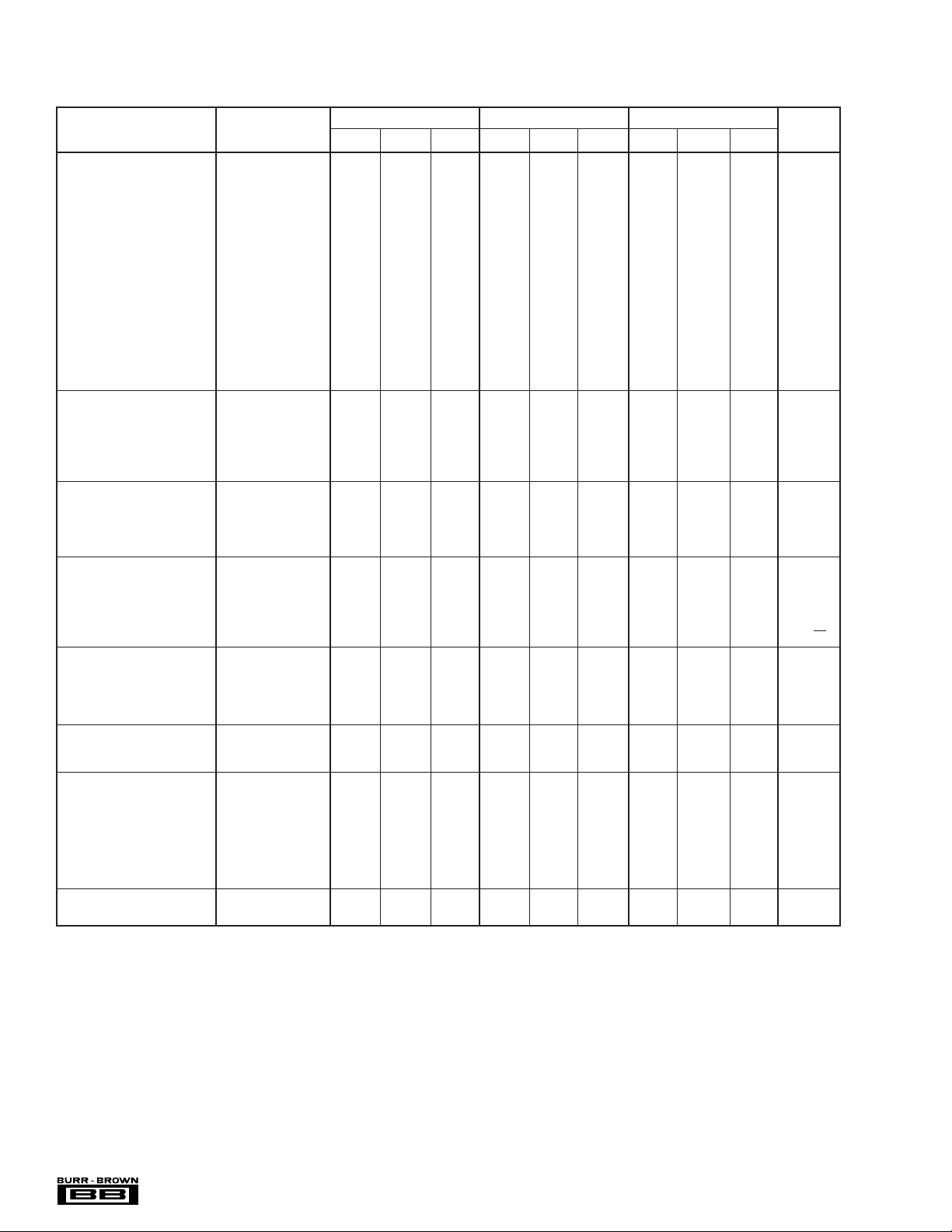
SPECIFICATIONS (Dual Supply)
At TA = T
PARAMETER CONDITIONS MIN TYP MAX MIN TYP MAX MIN TYP MAX UNITS
ACCURACY
Linearity Error T = 25°C ±3 ✻ ±2 LSB
Linearity Match ±4 ✻ ±2 LSB
Differential Linearity Error T = 25°C ±3 ±2 ±1 LSB
Monotonicity, T
Bipolar Zero Error
Bipolar Zero Error, T
Full-Scale Error T = 25°C ±0.025 ✻✻% of FSR
Full-Scale Error, T
Bipolar Zero Matching Channel-to-Channel ±0.024 ✻✻% of FSR
Full-Scale Matching Channel-to-Channel ±0.024 ✻✻% of FSR
Power Supply Rejection Ratio (PSRR)
ANALOG OUTPUT
Voltage Output V
Output Current ±5 ✻✻ mA
Maximum Load Capacitance 500 ✻✻pF
Short-Circuit Current ±20 ✻✻mA
Short-Circuit Duration To V
REFERENCE INPUT
Ref High Input Voltage Range
Ref Low Input Voltage Range –10
Ref High Input Current –0.3 2.6 ✻✻mA
Ref Low Input Current –3.2 –0.3 ✻✻mA
DYNAMIC PERFORMANCE
Settling Time To ±0.003%, 20V 9 11 ✻✻ ✻✻ µs
Channel-to-Channel Crosstalk See Figure 5 0.5 ✻✻LSB
Digital Feedthrough 2 ✻✻nV-s
Output Noise Voltage f = 10kHz 60 ✻✻nV/√Hz
DIGITAL INPUT
V
V
I
IH
I
IL
DIGITAL OUTPUT
V
V
POWER SUPPLY
V
V
V
I
DD
I
CC
I
SS
Power 170 200 ✻✻mW
TEMPERATURE RANGE
Specified Performance –40 +85 ✻✻✻✻°C
✻ Specifications same as grade to the left.
to T
MIN
, VCC = +15V, VDD = +5V, VSS = –15V, V
MAX
H = +10V, and V
REF
L = –10V, unless otherwise noted.
REF
DAC7744E DAC7744EB DAC7744EC
T
to T
MIN
MAX
T
to T
MIN
MAX
MIN
to T
MIN
MIN
MAX
to T
to T
T = 25°C ±0.01 ±0.025 ✻✻% of FSR
MAX
MAX
14 15 16 Bits
±4 ✻ ±3 LSB
±3 ±2 ±1 LSB
±0.05 ✻✻% of FSR
±0.05 ✻✻% of FSR
Matching
Matching
At Full Scale 25 ✻✻ppm/V
LV
REF
, V
or GND Indefinite ✻✻
SS
DD
V
L + 1.25
REF
H ✻✻✻✻V
REF
+10 ✻✻✻✻V
V
H – 1.25
REF
✻✻✻✻V
Output Step
IH
IL
0.7 • V
DD
0 0.3 • V
V
±10 ✻ µA
✻✻ V
DD
DD
✻ V
±10 ✻ µA
OH
OL
DD
CC
SS
IOH = –0.8mA 3.6 4.5 ✻✻ ✻✻ V
IOL = 1.6mA 0.3 0.4 ✻✻ ✻✻ V
+4.75 +5.0 +5.25 ✻✻✻✻✻✻ V
+14.25 +15.0 +15.75 ✻✻✻✻✻✻ V
–14.25 –15.0 –15.75 ✻✻✻✻✻✻ V
50 ✻✻µA
6 ✻✻mA
–5 ✻✻mA
The information provided herein is believed to be reliable; however, BURR-BROWN assumes no responsibility for inaccuracies or omissions. BURR-BROWN assumes
no responsibility for the use of this information, and all use of such information shall be entirely at the user’s own risk. Prices and specifications are subject to change
without notice. No patent rights or licenses to any of the circuits described herein are implied or granted to any third party. BURR-BROWN does not authorize or warrant
any BURR-BROWN product for use in life support devices and/or systems.
®
DAC7744
2
Page 3
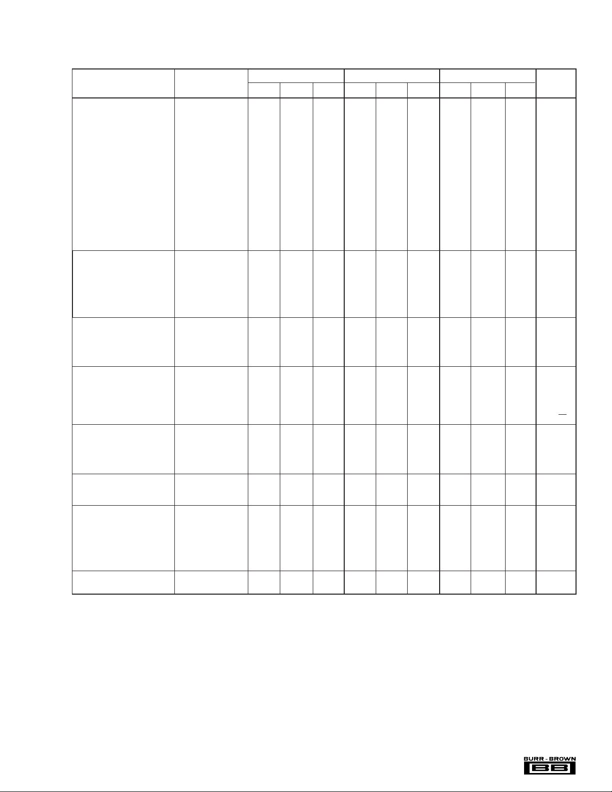
SPECIFICATIONS (Single Supply)
At TA = T
PARAMETER CONDITIONS MIN TYP MAX MIN TYP MAX MIN TYP MAX UNITS
ACCURACY
Linearity Error
Linearity Match ±4 ✻ ±2 LSB
Differential Linearity Error T = 25°C ±3 ±2 ±1 LSB
Monotonicity, T
Unipolar Zero T = 25°C ±0.01 ±0.025 ✻✻% of FSR
Unipolar Zero Error,
Full-Scale Error T = 25°C ±0.025 ✻✻% of FSR
Full-Scale Error,
Unipolar Zero Matching Channel-to-Channel ±0.024 ✻✻% of FSR
Full-Scale Matching Channel-to-Channel ±0.024 ✻✻% of FSR
Power Supply Rejection Ratio (PSRR)
ANALOG OUTPUT
Voltage Output V
Output Current ±5 ✻✻ mA
Maximum Load Capacitance 500 ✻✻pF
Short-Circuit Current ±20 ✻✻mA
Short-Circuit Duration To V
REFERENCE INPUT
Ref High Input Voltage Range
Ref Low Input Voltage Range 0
Ref High Input Current –0.3 1.0 ✻✻mA
Ref Low Input Current –1.5 –0.3 ✻✻mA
DYNAMIC PERFORMANCE
Settling Time To ±0.003%, 10V 8 10 ✻✻ ✻✻ µs
Channel-to-Channel Crosstalk See Figure 6 0.5 ✻✻LSB
Digital Feedthrough 2 ✻✻nV-s
Output Noise Voltage f = 10kHz 60 ✻✻nV/√Hz
DIGITAL INPUT
V
V
I
IH
I
IL
DIGITAL OUTPUT
V
V
POWER SUPPLY
V
V
V
I
DD
I
CC
Power 50 70 ✻✻mW
TEMPERATURE RANGE
Specified Performance –40 +85 ✻✻✻✻°C
✻ Specifications same as grade to the left.
NOTE: (1) If V
to T
MIN
, VCC = +15V, VDD = +5V, VSS = GND, V
MAX
H = +10V, and V
REF
L = +50mV, unless otherwise noted.
REF
DAC7744E DAC7744EB DAC7744EC
(1)
T
to T
MIN
MAX
T
to T
MIN
MAX
to T
MIN
MAX
T
to T
MIN
MAX
T
to T
MIN
MAX
T = 25°C ±3 ✻ ±2 LSB
±4 ✻ ±3 LSB
±3 ±2 ±1 LSB
14 15 16 Bits
±0.05 ✻✻% of FSR
±0.05 ✻✻% of FSR
Matching
Matching
At Full Scale 25 ✻✻ppm/V
L = 0V, VSS = 0V 0 V
REF
R = 10kΩ
, V
or GND Indefinite ✻✻
SS
CC
V
L + 1.25
REF
H ✻✻✻✻V
REF
+10 ✻✻✻✻V
V
H – 1.25
REF
✻✻✻✻V
Output Step
IH
IL
0.7 • V
DD
0 0.3 • V
V
±10 ✻ µA
✻✻ V
DD
DD
✻ V
±10 ✻ µA
OH
OL
DD
CC
SS
IOH = –0.8mA 3.6 4.5 ✻✻ ✻✻ V
IOL = 1.6mA 0.3 0.4 ✻✻ ✻✻ V
+4.75 +5.0 +5.25 ✻✻✻✻✻✻ V
+14.25 +15.0 +15.75 ✻✻✻✻✻✻ V
0 ✻✻V
50 ✻✻µA
3.5 ✻✻mA
= 0V, the specification applies at code 0021H and above, due to possible negative zero scale error.
SS
®
3
DAC7744
Page 4
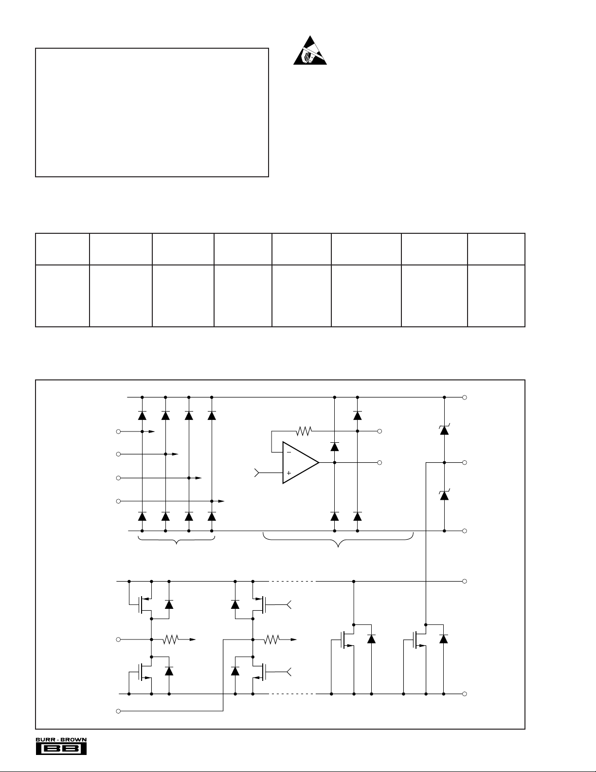
ABSOLUTE MAXIMUM RATINGS
V
to VSS...........................................................................–0.3V to +32V
CC
V
to AGND ...................................................................... –0.3V to +16V
CC
V
to AGND ...................................................................... +0.3V to –16V
SS
AGND
to DGND................................................................. –0.3V to +0.3V
V
to AGND ..................................................................... –9V to +11V
REFH
V
to AGND...................................................................... –11V to +9V
REFL
V
to GND ........................................................................... –0.3V to +6V
DD
V
to V
REFH
Digital Input Voltage to GND ................................... –0.3V to V
Digital Output Voltage to GND................................. –0.3V to V
Maximum Junction Temperature................................................... +150 °C
Operating Temperature Range ........................................–40°C to +85°C
Storage Temperature Range ......................................... –65°C to +150°C
Lead Temperature (soldering, 10s)............................................... +300°C
NOTE: (1) Stresses above those listed under “Absolute Maximum Ratings”
may cause permanent damage to the device. Exposure to absolute maximum
conditions for extended periods may affect device reliability.
L ........................................................................ –1V to 22V
REF
(1)
ELECTROSTATIC
DISCHARGE SENSITIVITY
This integrated circuit can be damaged by ESD. Burr-Brown
recommends that all integrated circuits be handled with
appropriate precautions. Failure to observe proper handling
and installation procedures can cause damage.
+ 0.3V
DD
+ 0.3V
DD
ESD damage can range from subtle performance degradation
to complete device failure. Precision integrated circuits may
be more susceptible to damage because very small parametric
changes could cause the device not to meet its published
specifications.
PACKAGE/ORDERING INFORMATION
LINEARITY DIFFERENTIAL PACKAGE SPECIFICATION
PRODUCT (LSB) (LSB) PACKAGE NUMBER RANGE NUMBER
ERROR NONLINEARITY DRAWING TEMPERATURE ORDERING TRANSPORT
DAC7744E ±4 ±3 48-Lead SSOP 333 –40°C to +85°C DAC7744E Rails
"" """ "DAC7744E/1K Tape and Reel
DAC7744EB ±4 ±2 48-Lead SSOP 333 –40°C to +85°C DAC7744EB Rails
"" """ "DAC7744EB/1K Tape and Reel
DAC7744EC ±3 ±1 48-Lead SSOP 333 –40°C to +85°C DAC7744EC Rails
"" """ "DAC7744EC/1K Tape and Reel
NOTE: (1) Models with a slash (/) are available only in Tape and Reel in the quantities indicated (e.g., /1K indicates 1000 devices per reel). Ordering 1000 pieces
of “DAC7744E/1K” will get a single 1000-piece Tape and Reel.
(1)
MEDIA
ESD PROTECTION CIRCUITS
RefH
RefH Sense
RefL Sense
RefL
Typ of Each
Logic Input Pin
1 of 2
V
CC
V
Sense
OUT
V
OUT
4
V
SS
1 of 4
V
DD
V
CC
AGND
V
SS
V
DD
Typ of Each
I/O Pin
®
DAC7744
DGND
DGND
4
Page 5
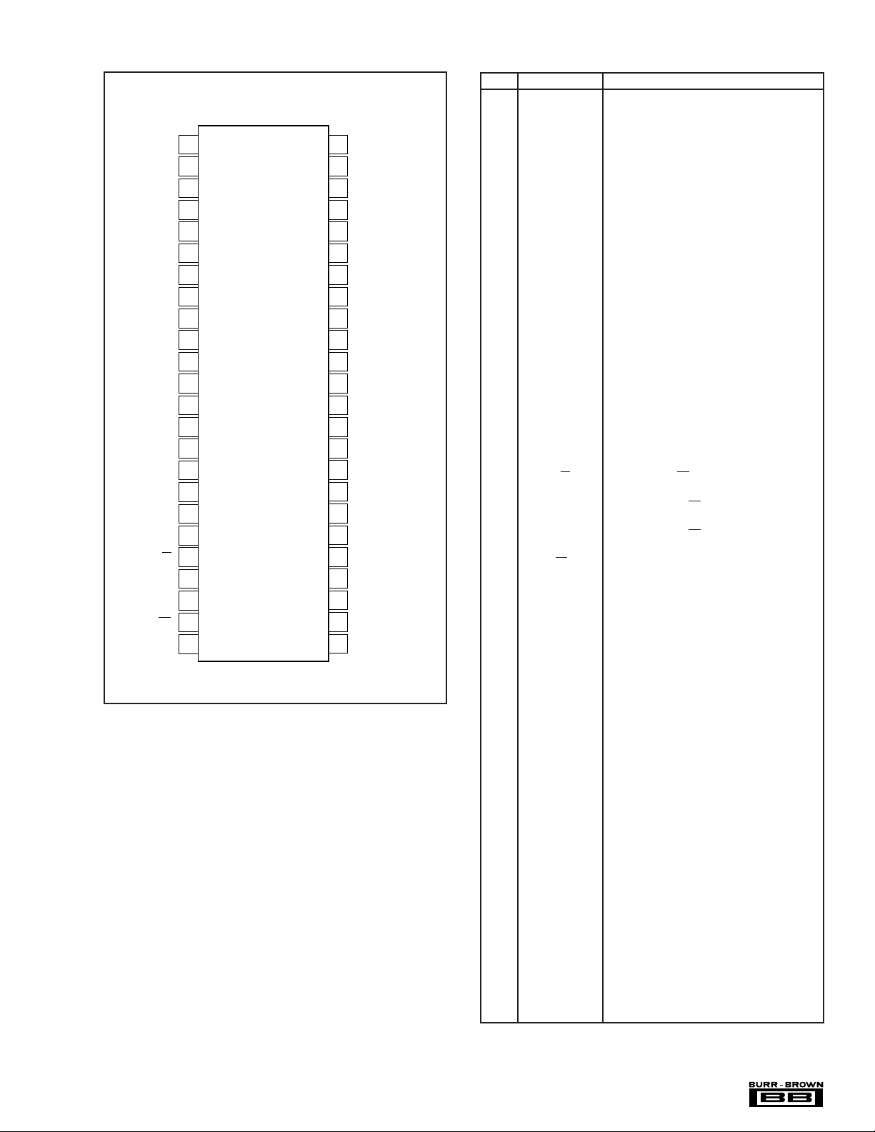
PIN CONFIGURATION
Top View SSOP
DB15 (MSB)
DB14
DB13
DB12
DB11
DB10
DB9
DB8
DB7
DB6
DB5
DB4
DB3
DB2
DB1
DB0 (LSB)
RSTSEL
RST
LOADDACs
R/W
A1
A0
CS
DGND
1
2
3
4
5
6
7
8
9
10
11
12
DAC7744
13
14
15
16
17
18
19
20
21
22
23
24
48
NC
47
NC
46
NC
45
NC
44
V
A Sense
OUT
43
V
A
OUT
42
V
L AB Sense
REF
41
V
L AB
REF
40
V
H AB
REF
39
V
H AB Sense
REF
38
V
B Sense
OUT
37
V
B
OUT
36
V
C Sense
OUT
35
V
C
OUT
34
V
H CD Sense
REF
33
V
H CD
REF
32
V
L CD
REF
31
V
L CD Sense
REF
30
V
D Sense
OUT
29
V
D
OUT
28
V
SS
27
AGND
26
V
CC
25
V
DD
PIN DESCRIPTIONS
PIN NAME DESCRIPTION
1 DB15 Data Bit 15, MSB
2 DB14 Data Bit 14
3 DB13 Data Bit 13
4 DB12 Data Bit 12
5 DB11 Data Bit 11
6 DB10 Data Bit 10
7 DB9 Data Bit 9
8 DB8 Data Bit 8
9 DB7 Data Bit 7
10 DB6 Data Bit 6
11 DB5 Data Bit 5
12 DB4 Data Bit 4
13 DB3 Data Bit 3
14 DB2 Data Bit 2
15 DB1 Data Bit 1
16 DB0 Data Bit 0, LSB
17 RSTSEL Reset Select. Determines the action of RST. If
18 RST Reset, Edge-Triggered. Depending on the state
19 LOADDACs DAC Output Registers Load Control. Rising edge
20 R/W Enabled by the CS, controls data read and write
21 A1 Enabled by the CS, in combination with A0
22 A0 Enabled by the CS, in combination with A1
23 CS Chip Select, Active LOW.
24 DGND Digital Ground
25 V
26 V
DD
CC
27 AGND Analog Ground
28 V
29 V
30 V
31 V
32 V
33 V
34 V
35 V
36 V
37 V
38 V
39 V
40 V
41 V
42 V
43 V
44 V
SS
OUT
D Sense DAC D’s Output Amplifier Inverting Input. Used
OUT
L CD Sense DAC C and D Reference Low Sense Input
REF
L CD DAC C and D Reference Low Input
REF
H CD DAC C and D Reference High Input
REF
H CD Sense DAC C and D Reference High Sense Input
REF
OUT
C Sense DAC C’s Output Amplifier Inverting Input. Used
OUT
OUT
B Sense DAC B’s Output Amplifier Inverting Input. Used
OUT
H AB Sense DAC A and B Reference High Sense Input
REF
H AB DAC A and B Reference High Input
REF
L AB DAC A and B Reference Low Input
REF
L AB Sense DAC A and B Reference Low Sense Input
REF
OUT
A Sense DAC A’s Output Amplifier Inverting Input. Used
OUT
45 NC No Connection
46 NC No Connection
47 NC No Connection
48 NC No Connection
HIGH, a RST command will set the DAC registers to mid-scale. If LOW, a RST command will
set the DAC registers to zero.
of RSTSEL, the DAC Input and Output registers
are set to either mid-scale or zero.
triggered.
from the input register.
selects the Individual DAC Input Registers.
selects the individual DAC input registers.
Positive Power Supply
Positive Power Supply
Negative Power Supply
D DAC D Voltage Output
to close the feedback loop at the load.
C DAC C Voltage Output
to close the feedback loop at the load.
B DAC B Voltage Output
to close the feedback loop at the load.
A DAC A Voltage Input
to close the feedback loop at the load.
®
5
DAC7744
Page 6
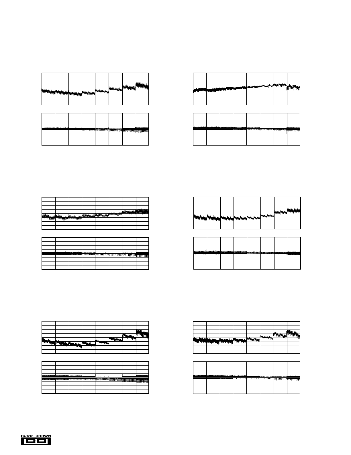
TYPICAL PERFORMANCE CURVES: VSS = 0V
At TA = +25°C, VDD = +5V, VCC = +15V, V
+25°C
DIFFERENTIAL LINEARITY ERROR vs CODE
2.0
1.5
1.0
0.5
0
–0.5
LE (LSB)DLE (LSB)
–1.0
–1.5
–2.0
2.0
1.5
1.0
0.5
0
–0.5
–1.0
–1.5
–2.0
0000H2000H4000H6000H8000
LINEARITY ERROR AND
(DAC A, +25°C)
Digital Input Code
SS
H
= 0, V
REFH
C000HE000HFFFF
A000
H
= +10V, and V
= 0V, representative unit, unless otherwise specified.
REFL
DIFFERENTIAL LINEARITY ERROR vs CODE
2.0
1.5
1.0
0.5
0
–0.5
LE (LSB)DLE (LSB)
–1.0
–1.5
–2.0
2.0
1.5
1.0
0.5
0
–0.5
–1.0
–1.5
–2.0
H
0000H2000H4000H6000H8000
LINEARITY ERROR AND
(DAC B, +25°C)
A000
H
H
Digital Input Code
C000HE000HFFFF
H
2.0
1.5
1.0
0.5
–0.5
LE (LSB)DLE (LSB)
–1.0
–1.5
–2.0
2.0
1.5
1.0
0.5
–0.5
–1.0
–1.5
–2.0
+85°C
2.0
1.5
1.0
0.5
–0.5
LE (LSB)DLE (LSB)
–1.0
–1.5
–2.0
2.0
1.5
1.0
0.5
–0.5
–1.0
–1.5
–2.0
DIFFERENTIAL LINEARITY ERROR vs CODE
LINEARITY ERROR AND
(DAC C, +25°C)
0
0
0000H2000H4000H6000H8000
Digital Input Code
LINEARITY ERROR AND
DIFFERENTIAL LINEARITY ERROR vs CODE
(DAC A, +85°C)
0
0
0000H2000H4000H6000H8000
Digital Input Code
DIFFERENTIAL LINEARITY ERROR vs CODE
LINEARITY ERROR AND
(DAC D, +25°C)
2.0
1.5
1.0
0.5
0
–0.5
LE (LSB)DLE (LSB)
–1.0
–1.5
–2.0
2.0
1.5
1.0
0.5
0
–0.5
–1.0
–1.5
–2.0
C000HE000HFFFF
A000
H
H
H
0000H2000H4000H6000H8000
H
C000HE000HFFFF
A000
H
H
Digital Input Code
LINEARITY ERROR AND
DIFFERENTIAL LINEARITY ERROR vs CODE
(DAC B, +85°C)
2.0
1.5
1.0
0.5
0
–0.5
LE (LSB)DLE (LSB)
–1.0
–1.5
–2.0
2.0
1.5
1.0
0.5
0
–0.5
–1.0
–1.5
C000HE000HFFFF
A000
H
H
H
–2.0
0000H2000H4000H6000H8000
C000HE000HFFFF
A000
H
H
H
Digital Input Code
®
DAC7744
6
Page 7
TYPICAL PERFORMANCE CURVES: VSS = 0V (Cont.)
2.0
1.5
1.0
0.5
0
–0.5
–1.0
–1.5
–2.0
2.0
1.5
1.0
0.5
0
–0.5
–1.0
–1.5
–2.0
LE (LSB)DLE (LSB)
LINEARITY ERROR AND
DIFFERENTIAL LINEARITY ERROR vs CODE
(DAC D, +85°C)
0000H2000H4000H6000H8000
H
Digital Input Code
A000
H
C000HE000HFFFF
H
At TA = +25°C, VDD = +5V, VCC = +15V, V
+85°C (cont.)
DIFFERENTIAL LINEARITY ERROR vs CODE
2.0
1.5
1.0
0.5
0
–0.5
LE (LSB)DLE (LSB)
–1.0
–1.5
–2.0
2.0
1.5
1.0
0.5
0
–0.5
–1.0
–1.5
–2.0
0000H2000H4000H6000H8000
LINEARITY ERROR AND
(DAC C, +85°C)
Digital Input Code
–40°C
DIFFERENTIAL LINEARITY ERROR vs CODE
2.0
1.5
1.0
0.5
0
–0.5
LE (LSB)DLE (LSB)
–1.0
–1.5
–2.0
2.0
1.5
1.0
0.5
0
–0.5
–1.0
–1.5
–2.0
0000H2000H4000H6000H8000
LINEARITY ERROR AND
(DAC A, –40°C)
Digital Input Code
SS
H
= 0, V
H
= +10V, and V
REFH
C000HE000HFFFF
A000
H
C000HE000HFFFF
A000
H
= 0V, representative unit, unless otherwise specified.
REFL
H
LINEARITY ERROR AND
DIFFERENTIAL LINEARITY ERROR vs CODE
2.0
1.5
1.0
0.5
0
–0.5
LE (LSB)DLE (LSB)
–1.0
–1.5
–2.0
2.0
1.5
1.0
0.5
0
–0.5
–1.0
–1.5
–2.0
H
0000H2000H4000H6000H8000
(DAC B, –40°C)
Digital Input Code
C000HE000HFFFF
A000
H
H
H
LE (LSB)DLE (LSB)
DIFFERENTIAL LINEARITY ERROR vs CODE
LINEARITY ERROR AND
(DAC C, –40°C)
2.0
1.5
1.0
0.5
0
–0.5
–1.0
–1.5
–2.0
2.0
1.5
1.0
0.5
0
–0.5
–1.0
–1.5
–2.0
0000H2000H4000H6000H8000
Digital Input Code
A000HC000HE000HFFFF
H
DIFFERENTIAL LINEARITY ERROR vs CODE
LINEARITY ERROR AND
(DAC D, –40°C)
2.0
1.5
1.0
0.5
0
–0.5
LE (LSB)DLE (LSB)
–1.0
–1.5
–2.0
2.0
1.5
1.0
0.5
0
–0.5
–1.0
–1.5
–2.0
H
0000H2000H4000H6000H8000
H
C000HE000HFFFF
A000
H
H
Digital Input Code
®
7
DAC7744
Page 8
TYPICAL PERFORMANCE CURVES: VSS = 0V (Cont.)
At TA = +25°C, VDD = +5V, VCC = +15V, V
SS
= 0, V
= +10V, and V
REFH
= 0V, representative unit, unless otherwise specified.
REFL
2
ZERO-SCALE ERROR vs TEMPERATURE
Code (0040H)Code (0021H)
1.5
DAC B
1
0.5
0
–0.5
–1
Zero-Scale Error (mV)
DAC A
–1.5
–2
–40 –30 –10 0–20 10 20 40 5030 70 80 9060
Temperature (°C)
CURRENT vs CODE
All DACs Sent to Indicated Code
(DAC A and B)
V
V
REFH
REFL
1.0
0.8
0.6
0.4
0.2
Current (mA)V
0
–0.2
REF
V
–0.4
0
–0.2
–0.4
–0.6
–0.8
Current (mA)
–1.0
REF
–1.2
–1.4
0000H2000H4000H6000H8000
Digital Input Code
H
DAC D
DAC C
C000HE000HFFFF
A000
H
2
Code (FFFFH)
1.5
DAC B
DAC D
1
0.5
0
FULL-SCALE ERROR vs TEMPERATURE
–0.5
DAC A
DAC C
–1
Positive Full-Scale Error (mV)
–1.5
–2
–40 –30 –10 0–20 10 20 40 5030 70 80 9060
Temperature (°C)
CURRENT vs CODE
All DACS Sent to Indicated Code
(DAC C and D)
V
V
REFH
REFL
A000
H
C000HE000HFFFF
H
H
1.0
0.8
0.6
0.4
0.2
Current (mA)V
0
–0.2
REF
V
–0.4
0
–0.2
–0.4
–0.6
–0.8
Current (mA)
–1.0
REF
–1.2
–1.4
H
0000H2000H4000H6000H8000
Digital Input Code
4.0
POWER SUPPLY CURRENT vs TEMPERATURE
Data = FFFFH (all DACs)
3.5
No Load
I
CC
3.0
2.5
2.0
1.5
1.0
0.5
Quiescent Current (mA)
0
–0.5
–40 –30 –10 0–20 10 20 40 5030 70 80 9060
Temperature (°C)
®
DAC7744
POSITIVE SUPPLY CURRENT
vs DIGITAL INPUT CODE
4.0
No Load
3.5
3.0
2.5
2.0
(mA)
CC
I
1.5
1.0
I
DD
0.5
0
0 2000H4000H6000H8000HA000HC000HE000HFFFF
H
Digital Input Code
8
Page 9

TYPICAL PERFORMANCE CURVES: VSS = 0V (Cont.)
+5V
LDAC
0
Time (2µs/div)
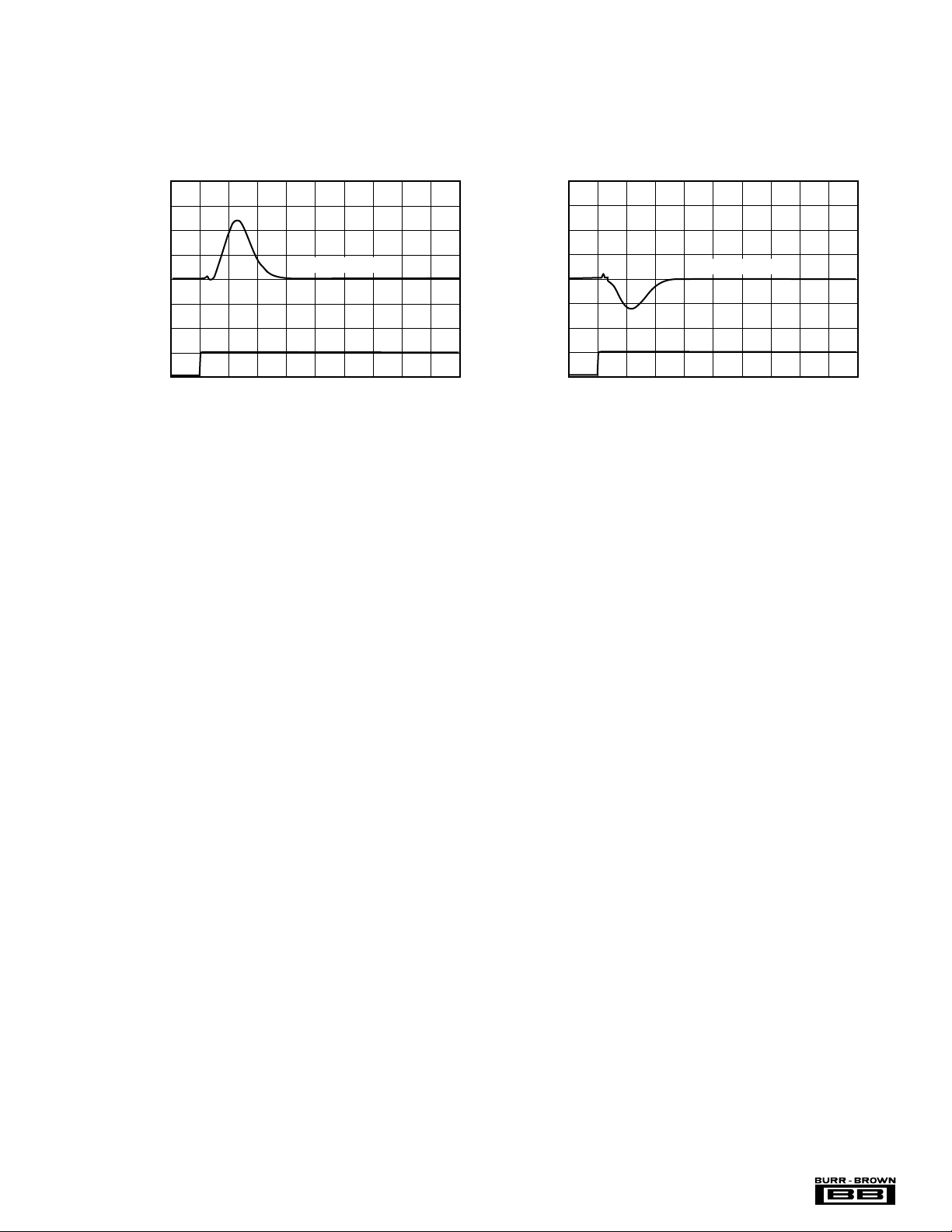
OUTPUT VOLTAGE vs SETTLING TIME
(+10V to 0V)
Output Voltage
Small-Signal Settling Time: 3LSB/div
Large-Signal Settling Time: 5V/div
120
100
80
60
40
20
0
Frequency (Hz)
100
1k
10k 100k
1M
OUTPUT NOISE VOLTAGE vs FREQUENCY
Noise (nV/√Hz)
+5V
LDAC
0
Time (1µs/div)
Output Voltage (50mV/div)
8000H to 7FFF
H
OUTPUT VOLTAGE
MIDSCALE GLITCH PERFORMANCE
At TA = +25°C, VDD = +5V, VCC = +15V, V
SS
= 0, V
= +10V, and V
REFH
= 0V, representative unit, unless otherwise specified.
REFL
OUTPUT VOLTAGE vs SETTLING TIME
Output Voltage
(0V to +10V)
Large-Signal Settling Time: 5V/div
Small-Signal Settling Time: 3LSB/div
Time (2µs/div)
OUTPUT VOLTAGE
MIDSCALE GLITCH PERFORMANCE
7FFFH to 8000
H
+5V
LDAC
0
Output Voltage (50mV/div)
Time (1µs/div)
BROADBAND NOISE
Noise Voltage (20µV/div)
Time (100µs/div)
BW = 10kHz
Code = 8000
+5V
LDAC
0
H
®
9
DAC7744
Page 10

TYPICAL PERFORMANCE CURVES: VSS = 0V (Cont.)
16
14
12
10
8
6
4
2
0
R
LOAD
(kΩ)
0.01
0.1
1 10 100
OUTPUT VOLTAGE vs R
LOAD
V
OUT
(V)
Source
Sink
At TA = +25°C, VDD = +5V, VCC = +15V, V
LOGIC SUPPLY CURRENT
vs LOGIC INPUT LEVEL FOR DATA BITS
12
10
8
6
4
Logic Supply Current (mA)
2
0
0 0.5 1 1.5 2 2.5 3 3.5 4 4.5 5
Logic Input Level for Data Bits (V)
SS
= 0, V
= +10V, and V
REFH
= 0V, representative unit, unless otherwise specified.
REFL
SINGLE-SUPPLY CURRENT LIMIT
vs INPUT CODE
20
15
Short to Ground
10
5
0
(mA)
OUT
I
–5
–10
–15
Short to V
CC
–20
0000H2000H4000H6000H8000HA000H0000HE000HFFFF
Input Code
POWER SUPPLY REJECTION RATIO vs FREQUENCY
0
–10
–20
–30
–40
–50
PSRR (dB)
–60
–70
–80
–90
H
100
DIGITAL-TO-ANALOG OUTPUT GLITCH
2LSB/div
1k
+15V
+5V
10k 100k 1M
Frequency (Hz)
Output Voltage (50mV/div)
Time (500ns/div)
+5V
CS
0
®
DAC7744
10
Page 11

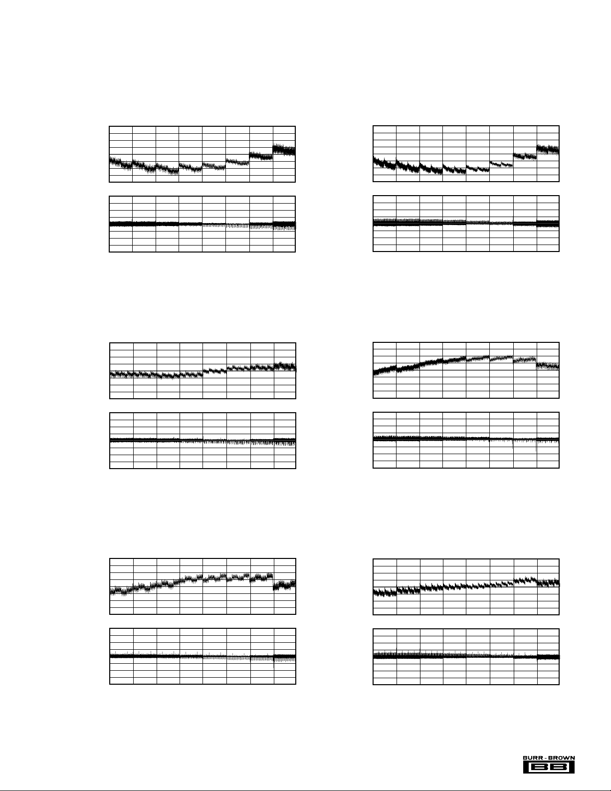
TYPICAL PERFORMANCE CURVES: VSS = –15V
2.0
1.5
1.0
0.5
0
–0.5
–1.0
–1.5
–2.0
2.0
1.5
1.0
0.5
0
–0.5
–1.0
–1.5
–2.0
LE (LSB)DLE (LSB)
LINEARITY ERROR AND
DIFFERENTIAL LINEARITY ERROR vs CODE
(DAC B, +25°C)
0000H2000H4000H6000H8000
H
Digital Input Code
A000
H
C000HE000HFFFF
H
DLE (LSB)
LINEARITY ERROR AND
DIFFERENTIAL LINEARITY ERROR vs CODE
(DAC D, +25°C)
0000H2000H4000H6000H8000
H
Digital Input Code
A000
H
C000HE000HFFFF
H
2.0
1.5
1.0
0.5
0
–0.5
–1.0
–1.5
–2.0
2.0
1.5
1.0
0.5
0
–0.5
–1.0
–1.5
–2.0
LE (LSB)
LE (LSB)DLE (LSB)
LINEARITY ERROR AND
DIFFERENTIAL LINEARITY ERROR vs CODE
(DAC B, +85°C)
0000H2000H4000H6000H8000
H
Digital Input Code
A000
H
C000HE000HFFFF
H
2.0
1.5
1.0
0.5
0
–0.5
–1.0
–1.5
–2.0
2.0
1.5
1.0
0.5
0
–0.5
–1.0
–1.5
–2.0
At TA = +25°C, VDD = +5V, VCC = +15V, VSS = –15V, V
= +10V, and V
REFH
= –10V, representative unit, unless otherwise specified.
REFL
+25°C
–0.5
LE (LSB)DLE (LSB)
–1.0
–1.5
–2.0
–0.5
–1.0
–1.5
–2.0
–0.5
LE (LSB)DLE (LSB)
–1.0
–1.5
–2.0
–0.5
–1.0
–1.5
–2.0
DIFFERENTIAL LINEARITY ERROR vs CODE
LINEARITY ERROR AND
(DAC A, +25°C)
2.0
1.5
1.0
0.5
0
2.0
1.5
1.0
0.5
0
0000H2000H4000H6000H8000
Digital Input Code
LINEARITY ERROR AND
DIFFERENTIAL LINEARITY ERROR vs CODE
(DAC C, +25°C)
2.0
1.5
1.0
0.5
0
2.0
1.5
1.0
0.5
0
0000H2000H4000H6000H8000
Digital Input Code
C000HE000HFFFF
A000
H
H
C000HE000HFFFF
A000
H
H
H
H
+85°C
LE (LSB)DLE (LSB)
DIFFERENTIAL LINEARITY ERROR vs CODE
LINEARITY ERROR AND
(DAC A, +85°C)
2.0
1.5
1.0
0.5
0
–0.5
–1.0
–1.5
–2.0
2.0
1.5
1.0
0.5
0
–0.5
–1.0
–1.5
–2.0
0000H2000H4000H6000H8000
Digital Input Code
C000HE000HFFFF
A000
H
H
H
®
11
DAC7744
Page 12

TYPICAL PERFORMANCE CURVES: VSS = –15V (Cont.)
At TA = +25°C, VDD = +5V, VCC = +15V, VSS = –15V, V
+85°C (cont.)
DIFFERENTIAL LINEARITY ERROR vs CODE
2.0
1.5
1.0
0.5
0
–0.5
LE (LSB)DLE (LSB)
–1.0
–1.5
–2.0
2.0
1.5
1.0
0.5
0
–0.5
–1.0
–1.5
–2.0
0000H2000H4000H6000H8000
LINEARITY ERROR AND
(DAC C, +85°C)
A000
H
H
Digital Input Code
–40°C
DIFFERENTIAL LINEARITY ERROR vs CODE
2.0
1.5
1.0
0.5
0
–0.5
LE (LSB)DLE (LSB)
–1.0
–1.5
–2.0
2.0
1.5
1.0
0.5
0
–0.5
–1.0
–1.5
–2.0
0000H2000H4000H6000H8000
LINEARITY ERROR AND
(DAC A, –40°C)
A000
H
Digital Input Code
H
= +10V, and V
REFH
C000HE000HFFFF
C000HE000HFFFF
= –10V, representative unit, unless otherwise specified.
REFL
LINEARITY ERROR AND
DIFFERENTIAL LINEARITY ERROR vs CODE
(DAC D, +85°C)
2.0
1.5
1.0
0.5
0
–0.5
LE (LSB)DLE (LSB)
–1.0
–1.5
–2.0
2.0
1.5
1.0
0.5
0
–0.5
–1.0
–1.5
–2.0
H
0000H2000H4000H6000H8000
Digital Input Code
LINEARITY ERROR AND
DIFFERENTIAL LINEARITY ERROR vs CODE
(DAC B, –40°C)
2.0
1.5
1.0
0.5
0
–0.5
LE (LSB)DLE (LSB)
–1.0
–1.5
–2.0
2.0
1.5
1.0
0.5
0
–0.5
–1.0
–1.5
–2.0
H
0000H2000H4000H6000H8000
Digital Input Code
C000HE000HFFFF
A000
H
H
C000HE000HFFFF
A000
H
H
H
H
DIFFERENTIAL LINEARITY ERROR vs CODE
LINEARITY ERROR AND
2.0
1.5
1.0
0.5
0
–0.5
LE (LSB)DLE (LSB)
–1.0
–1.5
–2.0
2.0
1.5
1.0
0.5
0
–0.5
–1.0
–1.5
–2.0
0000H2000H4000H6000H8000
®
DAC7744
(DAC C, –40°C)
A000
H
Digital Input Code
C000HE000HFFFF
H
DIFFERENTIAL LINEARITY ERROR vs CODE
LINEARITY ERROR AND
(DAC D, –40°C)
2.0
1.5
1.0
0.5
0
–0.5
LE (LSB)DLE (LSB)
–1.0
–1.5
–2.0
2.0
1.5
1.0
0.5
0
–0.5
–1.0
–1.5
–2.0
H
0000H2000H4000H6000H8000
H
C000HE000HFFFF
A000
H
H
Digital Input Code
12
Page 13

TYPICAL PERFORMANCE CURVES: VSS = –15V (Cont.)
2.0
1.5
1.0
0.5
0
–0.5
–1.0
–1.5
0.5
0
–0.5
–1.0
–1.5
–2.0
–2.5
–3.0
V
REF
Current (mA)V
REF
Current (mA)
CURRENT vs CODE
All DACs Sent to Indicated Code
(DAC C and D)
V
REFH
V
REFL
0000H2000H4000H6000H8000
H
Digital Input Code
A000
H
C000HE000HFFFF
H
2
1.5
1.0
0.5
0
–0.5
–1.0
–1.5
–2.0
Temperature (°C)
–40 –10 0–30 –20 9010 20 30 40 50 60 70 80
POSITIVE FULL-SCALE ERROR vs TEMPERATURE
(Code FFFF
H
)
Positive Full-Scale Error (mV)
DAC B
DAC A
DAC C
DAC D
7
6
5
4
3
2
1
0
–1
–2
–3
–4
–5
–6
–7
Temperature (°C)
–40 –10 0–30 –20 9010 20 30 40 50 60 70 80
POWER SUPPLY CURRENT vs TEMPERTURE
Quiescent Current (mA)
I
SS
I
CC
I
DD
Data = FFFF
H
(all DACs)
No Load
At TA = +25°C, VDD = +5V, VCC = +15V, VSS = –15V, V
CURRENT vs CODE
All DACs Sent to Indicated Code
(DAC A and B)
V
V
REFH
REFL
A000
H
H
2.0
1.5
1.0
0.5
0
Current (mA)V
-0.5
–1.0
REF
V
–1.5
0.5
0
–0.5
–1.0
–1.5
Current (mA)
–2.0
REF
–2.5
–3.0
0000H2000H4000H6000H8000
Digital Input Code
= +10V, and V
REFH
C000HE000HFFFF
= –10V, representative unit, unless otherwise specified.
REFL
H
BIPOLAR ZERO SCALE ERROR vs TEMPERATURE
2
1.5
1
DAC B
0.5
0
–0.5
DAC A
–1
Bipolar Zero Scale Error (mV)
–1.5
–2
–40 –20 100020406080
NEGATIVE FULL-SCALE ERROR vs TEMPERATURE
2
1.5
1.0
0.5
0
–0.5
–1.0
Negative Full-Scale Error (mV)
–1.5
–2.0
–40 –10 0–30 –20 9010 20 30 40 50 60 70 80
DAC B
DAC A
(Code 8000
)
H
DAC D
DAC C
Temperature (°C)
(Code 0000
)
H
DAC D
DAC C
Temperature (°C)
®
13
DAC7744
Page 14

TYPICAL PERFORMANCE CURVES: VSS = –15V (Cont.)
At TA = +25°C, VDD = +5V, VCC = +15V, VSS = –15V, V
= +10V, and V
REFH
= –10V, representative unit, unless otherwise specified.
REFL
(V)
OUT
V
–10
–15
15
OUTPUT VOLTAGE vs R
LOAD
7
6
10
Source
5
5
4
3
2
1
0
–5
Sink
(mA)
0
1
2
3
4
SUPPLY CURRENT vs CODE
I
CC
I
DD
I
SS
5
6
7
0.01
0.1
1 10 100
(kΩ)
R
LOAD
OUTPUT VOLTAGE vs SETTLING TIME
(–10V to +10V)
Large-Signal Settling Time: 5V/div
0000H2000H4000H6000H8000HA000HC000HE000HFFFF
Digital Input Code
OUTPUT VOLTAGE vs SETTLING TIME
(+10V to –10V)
Small-Signal Settling Time: 3LSB/div
H
Small-Signal Settling Time: 3LSB/div
Output Voltage
Time (2µs/div)
+5V
LDAC
0
Output Voltage
Large-Signal Settling Time: 5V/div
Time (2µs/div)
+5V
LDAC
0
DUAL SUPPLY CURRENT LIMIT vs INPUT CODE
20
Short to Ground
15
10
5
(mA)
0
OUT
I
–5
PSRR (dB)
–10
–15
–20
0000H2000H4000H6000H8000HA000HC000HE000HFFFF
H
Digital Input Code
POWER SUPPLY REJECTION RATIO vs FREQUENCY
0
–10
–20
–30
–40
–50
–60
–15V
+15V
–70
–80
–90
–100
100
1k
+5V
10k 100k 1M
Frequency (Hz)
®
DAC7744
14
Page 15
TYPICAL PERFORMANCE CURVES: VSS = –15V (Cont.)
At TA = +25°C, VDD = +5V, VCC = +15V, VSS = –15V, V
= +10V, and V
REFH
= –10V, representative unit, unless otherwise specified.
REFL
OUTPUT VOLTAGE
MID-SCALE GLITCH PERFORMANCE
Output Voltage (50mV/div)
7FFFH to 8000
Time (1µs/div)
OUTPUT VOLTAGE
MID-SCALE GLITCH PERFORMANCE
H
+5V
LDAC
0
Output Voltage (50mV/div)
8000H to 7FFF
Time (1µs/div)
H
+5V
LDAC
0
15
®
DAC7744
Page 16

THEORY OF OPERATION
The DAC7744 is a quad voltage output, 16-bit digital-toanalog converter (DAC). The architecture is an R-2R ladder
configuration with the three MSB’s segmented followed by
an operational amplifier that serves as a buffer. Each DAC
has its own R-2R ladder network, segmented MSBs and
output op amp (see Figure 1). The minimum voltage output
(zero scale) and maximum voltage output (full scale) are set
by the external voltage references (V
L and V
REF
REF
H, respectively). The digital input is a 16-bit parallel word and
the DAC input registers offer a readback capability. The
converters can be powered from either a single +15V supply
or a dual ±15V supply. The device offers a reset function
which immediately sets all DAC output voltages and DAC
registers to mid-scale code 8000H or to zero scale, code
0000H. See Figures 2 and 3 for the basic operation of the
DAC7744.
R
F
V
Sense
OUT
R
2R2R 2R 2R 2R 2R 2R 2R
2R
FIGURE 1. DAC7744 Architecture.
Reset DACs
Load DAC Registers
READ/WRITE
Chip Select
Data
Bus
Address
1
2
3
4
5
6
7
8
9
10
11
12
13
14
15
16
17
18
19
20
21
22
23
24
DB15 (MSB)
DB14
DB13
DB12
DB11
DB10
DB9
DB8
DB7
DB6
DB5
DB4
DB3
DB2
DB1
DB0 (LSB)
RSTSEL
RST
LOADDACS
R/W
A1
A0
CS
DGND
V
REF
V
REF
DAC7744
V
REF
V
REF
NC = No Connection
A Sense
V
OUT
V
L AB Sense
V
REF
V
REF
H AB Sense
B Sense
V
OUT
V
C Sense
V
OUT
V
H CD Sense
V
REF
V
REF
L CD Sense
D Sense
V
OUT
V
AGND
NC
NC
NC
NC
OUT
L AB
H AB
OUT
OUT
H CD
L CD
OUT
V
V
V
V
OUT
V
H
REF
V
H Sense
REF
V
L
REF
V
L Sense
REF
48
47
46
45
44
43
A
42
41
40
39
38
37
B
36
35
C
34
33
32
31
30
29
D
28
SS
27
26
CC
25
DD
0V to +10V
+10.000V
0V to +10V
0V to +10V
+10.000V
0V to +10V
0.1µF
0.1µF
+15V
+
1µF
+5V
+
1µF
FIGURE 2. Basic Single-Supply Operation of the DAC7744.
®
DAC7744
16
Page 17

+5V
Reset DACs
Load DAC Registers
READ/WRITE
Chip Select
Data
Bus
Address
1
2
3
4
5
6
7
8
9
10
11
12
13
14
15
16
17
18
19
20
21
22
23
24
DB15 (MSB)
DB14
DB13
DB12
DB11
DB10
DB9
DB8
DB7
DB6
DB5
DB4
DB3
DB2
DB1
DB0 (LSB)
RSTSEL
RST
LOADDACS
R/W
A1
A0
CS
DGND
V
REF
V
REF
DAC7744
V
REF
V
REF
NC = No Connection
V
A Sense
OUT
V
L AB Sense
V
REF
V
REF
H AB Sense
B Sense
V
OUT
V
V
C Sense
OUT
V
H CD Sense
H CD
V
REF
V
REF
L CD Sense
D Sense
V
OUT
V
AGND
OUT
L AB
H AB
OUT
OUT
L CD
OUT
V
V
V
NC
NC
NC
NC
48
47
46
45
44
43
A
42
41
40
39
38
37
B
36
35
C
34
33
32
31
30
29
D
28
SS
27
26
CC
25
DD
–10V to +10V
–10V
+10V
–10V to +10V
–10V to +10V
+10V
–10V
–10V to +10V
0.1µF
0.1µF
0.1µF
–15V
1µF
+
+15V
+
1µF
+5V
+
1µF
FIGURE 3. Basic Dual-Supply Operation of the DAC7744.
ANALOG OUTPUTS
When VSS = –15V (dual supply operation), the output amplifier can swing to within 4V of the supply rails, guaranteed
over the –40°C to +85°C temperature range. With VSS = 0V
(single-supply operation), and with R
also connected to
LOAD
ground, the output can swing to ground. Care must also be
taken when measuring the zero-scale error when VSS = 0V.
Since the output voltage cannot swing below ground, the
output voltage may not change for the first few digital input
codes (0000H, 0001H, 0002H, etc.), if the output amplifier has
a negative offset. At the negative limit of –5mV, the first
specified output starts at code 0021H.
Due to the high accuracy of these D/A converters, system
design problems such as grounding and contact resistance
become very important. A 16-bit converter with a 10V fullscale range has a 1LSB value of 152µV. With a load current
of 1mA, series wiring and connector resistance of only
150mΩ (RW2) will cause a voltage drop of 150µV, as shown
in Figure 4. To understand what this means in terms of a
system layout, the resistivity of a typical 1 ounce copper-clad
printed circuit board is 1/2 mΩ per square. For a 1mA load,
a 20 milli-inch wide printed circuit conductor 6 inches long
will result in a voltage drop of 150µV.
The DAC7744 offers a force and sense output configuration
for the high open-loop gain output amplifiers. This feature
allows the loop around the output amplifier to be closed at
the load, thus ensuring an accurate output voltage, as shown
in Figure 4.
DAC7744
V
V
REF
V
H AB Sense
REF
V
A Sense
OUT
L AB Sense
V
REF
V
REF
B Sense
OUT
V
H AB
V
NC
NC
NC
NC
OUT
L AB
OUT
48
47
46
R
45
44
43
A
42
41
40
39
38
37
B
W1
R
W2
R
W1
R
W2
V
+V
V
FIGURE 4. Analog Output Closed-Loop Configuration
(1/2 DAC7744). RW represents wiring resistances.
17
DAC7744
R
R
OUT
LOAD
+10V
OUT
LOAD
®
Page 18

REFERENCE INPUTS
The reference inputs, V
between V
+ 4V and V
SS
least 1.25V greater than V
each DAC is equal to V
L and V
REF
– 4V, provided that V
CC
REF
REFL
H, can be any voltage
REF
L. The minimum output of
plus a small offset voltage
REF
H is at
(essentially, the offset of the output op amp). The maximum
output is equal to V
H plus a similar offset voltage. Note
REF
that VSS (the negative power supply) must either be
connected to ground or must be in the range of –14.25V to
–15.75V. The voltage on VSS sets several bias points within
the converter. If VSS is not in one of these two configurations, the bias values may be in error and proper operation
of the device is not guaranteed.
The current into the V
H input and out of V
REF
L depends
REF
on the DAC output voltages and can vary from a few
48
NC
47
NC
46
NC
45
NC
DAC7744
V
V
REF
V
H AB Sense
REF
V
A Sense
OUT
L AB Sense
V
REF
V
REF
B Sense
OUT
V
H AB
V
OUT
L AB
OUT
44
43
A
42
41
40
39
38
37
B
V
OUT
1000pF
1000pF
V
OUT
microamps to approximately 2.0mA. The reference input
appears as a varying load to the reference. If the reference
can sink or source the required current, a reference buffer is
not required. The DAC7744 features a reference drive and
sense connection such that the internal errors caused by the
changing reference current and the circuit impedances can be
minimized. Figures 5 through 12 show different reference
configurations and the effect on the linearity and differential
linearity.
The analog supplies (or the analog supplies and the reference
power supplies) have to come up first. If the power supplies
for the reference come up first, then the VCC and V
supplies will be “powered from the reference via the ESD
protection diode”, see page 4.
+V
OPA2234
100Ω
100Ω
2200pF
2200pF
–10V
–V
+V
+10V
SS
FIGURE 5. Dual Supply Configuration-Buffered References, used for Dual Supply Performance Curves (1/2 DAC7744).
48
NC
47
NC
46
NC
45
NC
V
V
OUT
L AB
H AB
OUT
44
43
A
42
41
40
39
38
37
B
V
OUT
1000pF
1000pF
V
OUT
V
A Sense
OUT
DAC7744
V
L AB Sense
REF
V
REF
V
REF
V
H AB Sense
REF
V
B Sense
OUT
NOTE: V
drops across the 100Ω resistor and the output stage of the buffer op amp.
L has been chosen to be 50mV to allow for current sinking voltage
REF
100Ω
100Ω
2200pF
2200pF
+V
OPA350
OPA227
2kΩ
+0.050V
99kΩ
+V
+10V
FIGURE 6. Single-Supply Buffered Reference with a Reference Low of 50mV Used for Single-Supply Performance Curves
(1/2 DAC7744).
®
DAC7744
18
Page 19

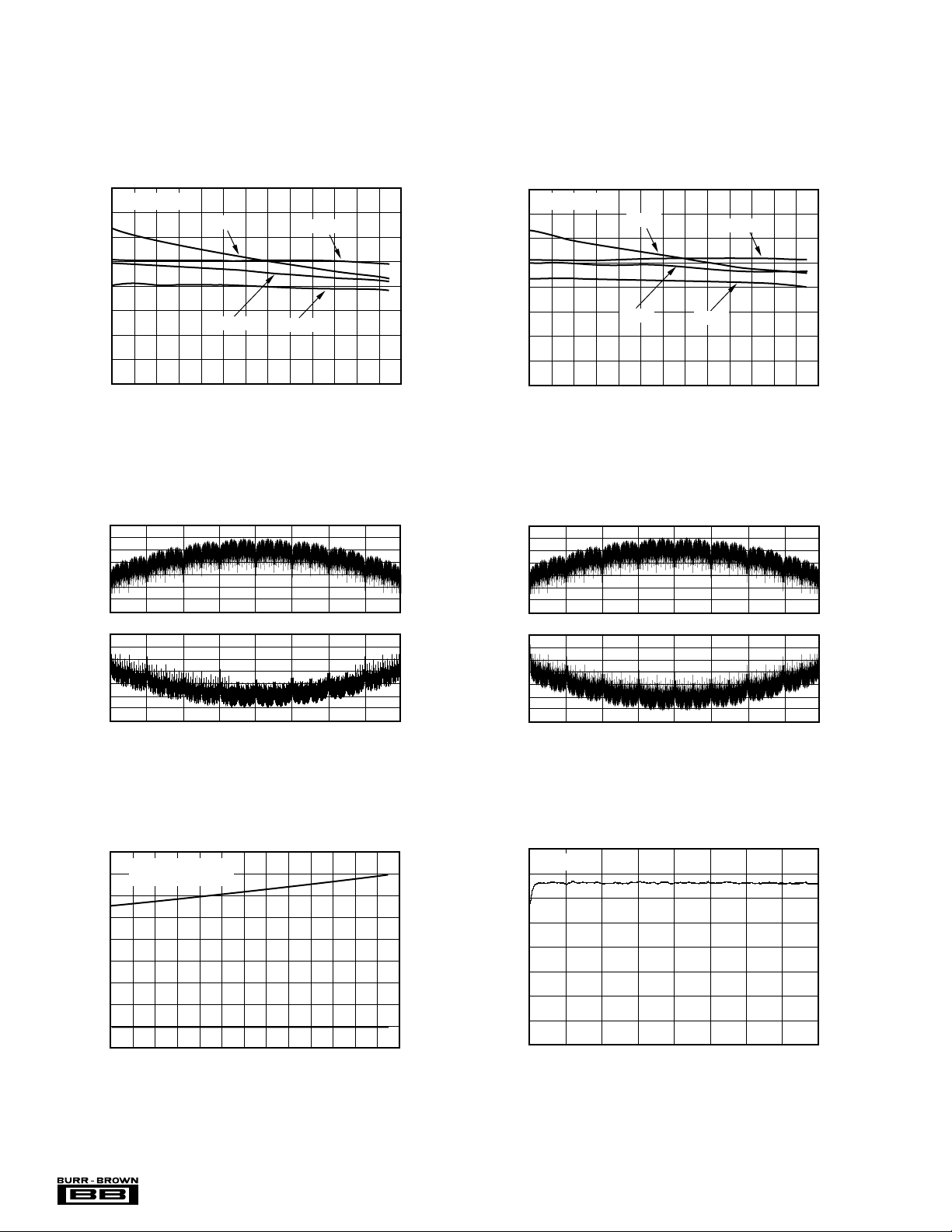
DIFFERENTIAL LINEARITY ERROR vs CODE
LINEARITY ERROR AND
2.0
1.5
1.0
0.5
0
–0.5
LE (LSB)DLE (LSB)
–1.0
–1.5
–2.0
1.0
0.5
0
–0.5
–1.0
0000H2000H4000H6000H8000
(DAC A, +25°C)
A000
H
Digital Input Code
C000HE000HFFFF
H
DIFFERENTIAL LINEARITY ERROR vs CODE
LINEARITY ERROR AND
(DAC B, +25°C)
2.0
1.5
1.0
0.5
0
–0.5
LE (LSB)DLE (LSB)
–1.0
–1.5
–2.0
1.0
0.5
0
–0.5
–1.0
H
0000H2000H4000H6000H8000
H
C000HE000HFFFF
A000
H
H
Digital Input Code
DIFFERENTIAL LINEARITY ERROR vs CODE
DIFFERENTIAL LINEARITY ERROR vs CODE
(DAC C, +25°C)
LINEARITY ERROR AND
2.0
1.5
1.0
0.5
0
–0.5
LE (LSB)DLE (LSB)
–1.0
–1.5
–2.0
1.0
0.5
0
–0.5
–1.0
0000H2000H4000H6000H8000
C000HE000HFFFF
A000
H
H
H
2.0
1.5
1.0
0.5
0
–0.5
LE (LSB)DLE (LSB)
–1.0
–1.5
–2.0
1.0
0.5
0
–0.5
–1.0
0000H2000H4000H6000H8000
Digital Input Code
FIGURE 7. Integral Linearity and Differential Linearity Error Curves for Figure 8.
48
NC
47
NC
46
NC
45
NC
DAC7744
V
OUT
L AB Sense
V
REF
H AB Sense
V
REF
V
OUT
A Sense
V
REF
V
REF
B Sense
V
H AB
V
OUT
L AB
OUT
44
43
A
42
41
40
39
38
37
B
V
OUT
100Ω
1000pF
100Ω
1000pF
V
OUT
2200pF
2200pF
LINEARITY ERROR AND
(DAC D, +25°C)
A000
H
Digital Input Code
+V
OPA2234
C000HE000HFFFF
H
–5V
–V
+V
+5V
H
FIGURE 8. Dual-Supply Buffered Referenced with V
L = –5V and V
REF
19
–V
H = +5V (1/2 DAC7744).
REF
®
DAC7744
Page 20

48
NC
47
NC
46
NC
+V
1kΩ
OPA350
0.05V
99kΩ
OPA227
DAC7744
V
V
REF
V
REF
V
NC
A Sense
OUT
V
OUT
L AB Sense
L AB
V
REF
H AB
V
REF
H AB Sense
B Sense
OUT
V
OUT
45
44
43
A
42
41
40
39
38
37
B
V
OUT
100Ω
1000pF
100Ω
1000pF
V
OUT
2200pF
2200pF
FIGURE 9. Single-Supply Buffered Reference with a Reference Low of 50mV and Reference High of +5V.
+V
+5V
DIFFERENTIAL LINEARITY ERROR vs CODE
LINEARITY ERROR AND
2.0
1.5
1.0
0.5
0
–0.5
LE (LSB)DLE (LSB)
–1.0
–1.5
–2.0
1.0
0.5
0
–0.5
–1.0
0000H2000H4000H6000H8000
LINEARITY ERROR AND
DIFFERENTIAL LINEARITY ERROR vs CODE
2.0
1.5
1.0
0.5
0
–0.5
LE (LSB)DLE (LSB)
–1.0
–1.5
–2.0
1.0
0.5
0
–0.5
–1.0
0000H2000H4000H6000H8000
(DAC A, +25°C)
A000
H
Digital Input Code
(DAC C, +25°C)
A000
H
Digital Input Code
C000HE000HFFFF
H
C000HE000HFFFF
H
DIFFERENTIAL LINEARITY ERROR vs CODE
LINEARITY ERROR AND
(DAC B, +25°C)
2.0
1.5
1.0
0.5
0
–0.5
LE (LSB)DLE (LSB)
–1.0
–1.5
–2.0
1.0
0.5
0
–0.5
–1.0
H
0000H2000H4000H6000H8000
A000
H
C000HE000HFFFF
H
H
Digital Input Code
LINEARITY ERROR AND
DIFFERENTIAL LINEARITY ERROR vs CODE
(DAC D, +25°C)
2.0
1.5
1.0
0.5
0
–0.5
LE (LSB)DLE (LSB)
–1.0
–1.5
–2.0
1.0
0.5
0
–0.5
–1.0
H
0000H2000H4000H6000H8000
A000
H
C000HE000HFFFF
H
H
Digital Input Code
FIGURE 10. Integral Linearity and Differential Linearity Error Curves for Figure 9.
®
DAC7744
20
Page 21

A1 A0 R/W CS RST RSTSEL
LLLLXXX Write Hold Write Input A
L H L L X X X Write Hold Write Input B
H L L L X X X Write Hold Write Input C
H H L L X X X Write Hold Write Input D
L L H L X X X Read Hold Read Input A
L H H L X X X Read Hold Read Input B
H L H L X X X Read Hold Read Input C
H H H L X X X Read Hold Read Input D
XXXHXX↑ Hold Write Update All
X X X H X X H Hold Hold Hold All
XXXX↑ L X Reset to Zero Reset to Zero All
XXXX↑ H X Reset to Midscale Reset to Midscale All
LOADDACS
INPUT DAC
REGISTER REGISTER MODE DAC
TABLE I. DAC7744 Logic Truth Table.
DIGITAL INTERFACE
Table I shows the basic control logic for the DAC7744. Note
that each DAC register is edge triggered and not level
triggered. When the LOADDACS signal is transitioned to
HIGH, the digital word currently in the DAC register is
latched. The first set of registers (the input registers) are
triggered via the A0, A1, R/W, and CS inputs. Only one of
these registers is transparent at any given time.
The double-buffered architecture is designed mainly so that
each DAC input register can be written to at any time and
then all DAC voltages updated simultaneously by the rising
edge of LOADDACS. It also allows a DAC input register to
be written to at any point then the DAC output voltages can
be synchronously changed via a trigger signal connected to
LOADDACS.
DIGITAL TIMING
Figure 11 and Table II provide detailed timing for the digital
interface of the DAC7744.
DIGITAL INPUT CODING
The DAC7744 input data is in Straight Binary format. The
output voltage is given by Equation 1.
VHVLN
VVL
=+
OUT REF
()
–•
REF REF
,65 536
(1)
DIGITALLY-PROGRAMMABLE
CURRENT SOURCE
The DAC7744 offers a unique set of features that allows a
wide range of flexibility in designing applications circuits
such as programmable current sources. The DAC7744 offers
both a differential reference input as well as an open-loop
configuration around the output amplifier. The open-loop
configuration around the output amplifier allows transistor
to be placed within the loop to implement a digitallyprogrammable, uni-directional current source. The availability of a differential reference also allows programmability
for both the full-scale and zero-scale currents. The output
current is calculated as:
I
OUT
VHVLRN
=
–
REF REF
SENSE
VLR
+
()
REF SENSE
•
,/65 536
(2)
Figure 12 shows a DAC7744 in a 4-to-20mA current output
configuration. The output current can be determined by
Equation 3:
(3)
I
OUT
51
–
VV N V
=
250 65 536
•
1
+
,ΩΩ
250
where N is the digital input code. This equation does not
include the effects of offset (zero scale) or gain (full scale)
errors.
At full scale, the output current is 16mA plus the 4mA for
the zero current. At zero scale, the output current is the offset
current of 4mA (1V/250Ω).
21
DAC7744
®
Page 22

CS
R/W
A0/A1
Data Out
t
RDS
t
AS
Data Read Timing
t
RCS
Data Valid
t
CSD
RESET SEL
t
t
t
RDH
AH
DZ
RST
LOADDACS
t
SS
t
RSS
CS
R/W
A0/A1
Data In
V
OUT
t
RSH
t
WCS
t
WS
t
AS
t
LWD
t
DS
t
WH
t
AH
t
t
LS
LH
t
LX
t
DH
t
S
±0.003% of FSR
Error Band
Data Write Timing
±0.003% of FSR
t
SH
Error Band
+FS
,RESET SEL LOW
V
OUT
–FS
+FS
V
,RESET SEL HIGH
OUT
–FS
FIGURE 11. Digital Input and Output Timing.
SYMBOL DESCRIPTION MIN TYP MAX UNITS
t
t
t
RDH
t
t
WCS
t
t
t
t
t
t
LWD
t
t
t
RCS
RDS
t
DZ
CSD
WS
WH
t
AS
AH
t
LS
t
LH
t
LX
DS
DH
t
SS
SH
RSS
RSH
t
CS HIGH to Data Bus in High Impedance 10 70 ns
S
CS LOW for Read 100 ns
R/W HIGH to CS LOW 10 ns
R/W HIGH after CS HIGH 10 ns
CS LOW to Data Bus Valid 85 130 ns
CS LOW for Write 40 ns
R/W LOW to CS LOW 0 ns
R/W LOW after CS HIGH 10 ns
Address Valid to CS LOW 0 ns
Address Valid after CS HIGH 15 ns
CS LOW to LOADDACS HIGH 40 ns
CS LOW after LOADDACS HIGH 80 ns
LOADDACS HIGH 40 ns
Data Valid to CS LOW 0 ns
Data Valid after CS HIGH 15 ns
LOADDACS LOW 40 ns
RSTSEL Valid Before RESET HIGH 0 ns
RSTSEL Valid After RESET HIGH 120 ns
RESET LOW Before RESET HIGH 10 ns
RESET LOW After RESET HIGH 10 ns
Settling Time 11 µs
MS
DAC7744 Reset Timing
TABLE II. Timing Specifications (TA = –40°C to +85°C).
®
DAC7744
22
Page 23

DAC7744
V
V
REF
V
REF
V
NC
NC
NC
NC
A Sense
OUT
V
OUT
L AB Sense
V
L AB
REF
V
H AB
REF
H AB Sense
B Sense
OUT
V
OUT
I
OUT
V
PROGRAMMED
48
47
R
SENSE
250Ω
46
45
+V
44
43
A
42
41
1000pF
40
39
1000pF
38
37
B
100Ω
100Ω
2200pF
2200pF
OPA2350
20kΩ
+1.0V
80kΩ
+V
FIGURE 12. 4-to-20mA Digitally-Controlled Current Source (1/2 DAC7744).
I
OUT
V
PROGRAMMED
R
SENSE
250Ω
GND
23
®
DAC7744
Page 24

PACKAGE OPTION ADDENDUM
www.ti.com
14-Aug-2006
PACKAGING INFORMATION
Orderable Device Status
(1)
Package
Type
Package
Drawing
Pins Package
Qty
Eco Plan
DAC7744E ACTIVE SSOP DL 48 30 TBD CU NIPDAU Level-3-220C-168 HR
DAC7744E/1K ACTIVE SSOP DL 48 1000 TBD CU NIPDAU Level-3-220C-168 HR
DAC7744E/1KG4 ACTIVE SSOP DL 48 1000 Green (RoHS &
no Sb/Br)
DAC7744EB ACTIVE SSOP DL 48 30 TBD CU NIPDAU Level-3-220C-168 HR
DAC7744EB/1K ACTIVE SSOP DL 48 1000 TBD CU NIPDAU Level-3-220C-168 HR
DAC7744EB/1KG4 ACTIVE SSOP DL 48 Green (RoHS &
no Sb/Br)
DAC7744EBG4 ACTIVE SSOP DL 48 30 Green (RoHS &
no Sb/Br)
DAC7744EC ACTIVE SSOP DL 48 30 TBD CU NIPDAU Level-3-220C-168 HR
DAC7744EC/1K ACTIVE SSOP DL 48 1000 TBD CU NIPDAU Level-3-220C-168 HR
DAC7744EC/1KG4 ACTIVE SSOP DL 48 1000 Green (RoHS &
no Sb/Br)
DAC7744ECG4 ACTIVE SSOP DL 48 30 Green (RoHS &
no Sb/Br)
DAC7744EG4 ACTIVE SSOP DL 48 30 Green (RoHS &
no Sb/Br)
(1)
The marketing status values are defined as follows:
ACTIVE: Product device recommended for new designs.
LIFEBUY: TI has announced that the device will be discontinued, and a lifetime-buy period is in effect.
NRND: Not recommended for new designs. Device is in production to support existing customers, but TI does not recommend using this part in
a new design.
PREVIEW: Device has been announced but is not in production. Samples may or may not be available.
OBSOLETE: TI has discontinued the production of the device.
(2)
Lead/Ball Finish MSL Peak Temp
CU NIPDAU Level-3-260C-168 HR
CU NIPDAU Level-3-260C-168 HR
CU NIPDAU Level-3-260C-168 HR
CU NIPDAU Level-3-260C-168 HR
CU NIPDAU Level-3-260C-168 HR
CU NIPDAU Level-3-260C-168 HR
(3)
(2)
Eco Plan - The planned eco-friendly classification: Pb-Free (RoHS), Pb-Free (RoHS Exempt), or Green (RoHS & no Sb/Br) - please check
http://www.ti.com/productcontent for the latest availability information and additional product content details.
TBD: The Pb-Free/Green conversion plan has not been defined.
Pb-Free (RoHS): TI's terms "Lead-Free" or "Pb-Free" mean semiconductor products that are compatible with the current RoHS requirements
for all 6 substances, including the requirement that lead not exceed 0.1% by weight in homogeneous materials. Where designed to be soldered
at high temperatures, TI Pb-Free products are suitable for use in specified lead-free processes.
Pb-Free (RoHS Exempt): This component has a RoHS exemption for either 1) lead-based flip-chip solder bumps used between the die and
package, or 2) lead-based die adhesive used between the die and leadframe. The component is otherwise considered Pb-Free (RoHS
compatible) as defined above.
Green (RoHS & no Sb/Br): TI defines "Green" to mean Pb-Free (RoHS compatible), and free of Bromine (Br) and Antimony (Sb) based flame
retardants (Br or Sb do not exceed 0.1% by weight in homogeneous material)
(3)
MSL, Peak Temp. -- The Moisture Sensitivity Level rating according to the JEDEC industry standard classifications, and peak solder
temperature.
Important Information and Disclaimer:The information provided on this page represents TI's knowledge and belief as of the date that it is
provided. TI bases its knowledge and belief on information provided by third parties, and makes no representation or warranty as to the
accuracy of such information. Efforts are underway to better integrate information from third parties. TI has taken and continues to take
reasonable steps to provide representative and accurate information but may not have conducted destructive testing or chemical analysis on
incoming materials and chemicals. TI and TI suppliers consider certain information to be proprietary, and thus CAS numbers and other limited
information may not be available for release.
In no event shall TI's liability arising out of such information exceed the total purchase price of the TI part(s) at issue in this document sold by TI
to Customer on an annual basis.
Addendum-Page 1
Page 25

IMPORTANT NOTICE
Texas Instruments Incorporated and its subsidiaries (TI) reserve the right to make corrections, modifications,
enhancements, improvements, and other changes to its products and services at any time and to discontinue
any product or service without notice. Customers should obtain the latest relevant information before placing
orders and should verify that such information is current and complete. All products are sold subject to TI’s terms
and conditions of sale supplied at the time of order acknowledgment.
TI warrants performance of its hardware products to the specifications applicable at the time of sale in
accordance with TI’s standard warranty. Testing and other quality control techniques are used to the extent TI
deems necessary to support this warranty . Except where mandated by government requirements, testing of all
parameters of each product is not necessarily performed.
TI assumes no liability for applications assistance or customer product design. Customers are responsible for
their products and applications using TI components. To minimize the risks associated with customer products
and applications, customers should provide adequate design and operating safeguards.
TI does not warrant or represent that any license, either express or implied, is granted under any TI patent right,
copyright, mask work right, or other TI intellectual property right relating to any combination, machine, or process
in which TI products or services are used. Information published by TI regarding third-party products or services
does not constitute a license from TI to use such products or services or a warranty or endorsement thereof.
Use of such information may require a license from a third party under the patents or other intellectual property
of the third party, or a license from TI under the patents or other intellectual property of TI.
Reproduction of information in TI data books or data sheets is permissible only if reproduction is without
alteration and is accompanied by all associated warranties, conditions, limitations, and notices. Reproduction
of this information with alteration is an unfair and deceptive business practice. TI is not responsible or liable for
such altered documentation.
Resale of TI products or services with statements different from or beyond the parameters stated by TI for that
product or service voids all express and any implied warranties for the associated TI product or service and
is an unfair and deceptive business practice. TI is not responsible or liable for any such statements.
Following are URLs where you can obtain information on other Texas Instruments products and application
solutions:
Products Applications
Amplifiers amplifier.ti.com Audio www.ti.com/audio
Data Converters dataconverter.ti.com Automotive www.ti.com/automotive
DSP dsp.ti.com Broadband www.ti.com/broadband
Interface interface.ti.com Digital Control www.ti.com/digitalcontrol
Logic logic.ti.com Military www.ti.com/military
Power Mgmt power.ti.com Optical Networking www.ti.com/opticalnetwork
Microcontrollers microcontroller.ti.com Security www.ti.com/security
Low Power Wireless www.ti.com/lpw Telephony www.ti.com/telephony
Video & Imaging www.ti.com/video
Wireless www.ti.com/wireless
Mailing Address: Texas Instruments
Post Office Box 655303 Dallas, Texas 75265
Copyright 2006, Texas Instruments Incorporated
 Loading...