

Page 1
查询DAC7642供应商
DAC7642
DAC7643
SBAS233 – DECEMBER 2001
16-Bit, Dual Voltage Output
DIGITAL-TO-ANALOG CONVERTER
DAC7642
DAC7643
FEATURES
● LOW POWER: 4mW
● UNIPOLAR OR BIPOLAR OPERATION
● SETTLING TIME: 10µs to 0.003% FSR
● 15-BIT LINEARITY AND MONOTONICITY:
–40°C to +85°C
● RESET TO MID-SCALE (DAC7642) OR
ZERO-SCALE (DAC7643)
● DATA READBACK
● DOUBLE-BUFFERED DATA INPUTS
APPLICATIONS
● PROCESS CONTROL
● CLOSED-LOOP SERVO-CONTROL
● MOTOR CONTROL
● DATA ACQUISITION SYSTEMS
● DAC-PER-PIN PROGRAMMERS
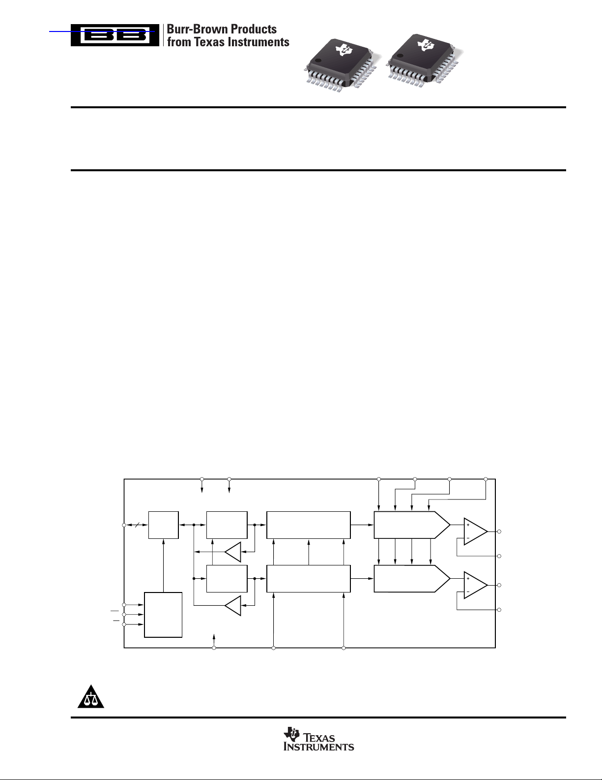
V
V
DAC7642
DAC7643
SS
CC
DESCRIPTION
The DAC7642 and DAC7643 are dual channel, 16-bit, voltage output Digital-to-Analog Converters (DACs) which provide 15-bit monotonic performance over the specified temperature range. They accept 16-bit parallel input data, have
double-buffered DAC input logic (allowing simultaneous update of all DACs), and provide a readback mode of the
internal input registers. Programmable asynchronous reset
clears all registers to a mid-scale code of 8000
or to a zero-scale code of 0000
(DAC7643). These DACs
H
can operate from a single +5V supply or from +5V and –5V
supplies, providing an output range of 0 to +2.5V or –2.5V to
+2.5V, respectively.
Low power and small size per DAC make the DAC7642 and
DAC7643 ideal for automatic test equipment, DAC-per-pin
programmers, data acquisition systems, and closed-loop
servo-control. The DAC7642 and DAC7643 are available in
a LQFP-32 package and specified over a –40°C to +85°C
temperature range.
V
REF
Sense
L
V
L V
REF
REF
V
REF
Sense
H
H
(DAC7642)
H
16
DATA I/O
DACSEL
CS
R/W
Please be aware that an important notice concerning availability, standard warranty, and use in critical applications of
Texas Instruments semiconductor products and disclaimers thereto appears at the end of this data sheet.
PRODUCTION DATA information is current as of publication date.
Products conform to specifications per the terms of Texas Instruments
standard warranty. Production processing does not necessarily include
testing of all parameters.
I/O
Buffer
Control
Logic
Input
Register A
Input
Register B
GND
RST
DAC
Register A
DAC
Register B
www.ti.com
LOADDACS
DAC A
DAC B
Copyright © 2001, Texas Instruments Incorporated
V
V
V
V
OUT
OUTA
OUT
OUTB
A
Sense
B
Sense
Page 2
ABSOLUTE MAXIMUM RATINGS
V
to VSS............................................................................. –0.3V to 11V
CC
V
to GND .......................................................................... –0.3V to 5.5V
CC
V
to VSS.............................................................–0.3V to (V
REFL
V
to V
CC
V
REFH
Digital Input Voltage to GND ................................... –0.3V to V
Digital Output Voltage to GND................................. –0.3V to V
Maximum Junction Temperature................................................... +150°C
Operating Temperature Range ........................................–40°C to +85°C
Storage Temperature Range ......................................... –65°C to +125°C
Lead Temperature (soldering, 10s)............................................... +300°C
NOTE: (1) Stresses above those listed under “Absolute Maximum Ratings”
may cause permanent damage to the device. Exposure to absolute maximum
conditions for extended periods may affect device reliability.
H ............................................................ –0.3V to (V
REF
to V
L ......................................................... –0.3V to (V
REF
(1)
ELECTROSTATIC
DISCHARGE SENSITIVITY
– VSS)
CC
CC
CC
+ 0.3V
CC
+ 0.3V
CC
– VSS)
– VSS)
This integrated circuit can be damaged by ESD. Texas Instruments recommends that all integrated circuits be handled with
appropriate precautions. Failure to observe proper handling
and installation procedures can cause damage.
ESD damage can range from subtle performance
degradation to complete device failure. Precision integrated
circuits may be more susceptible to damage because very
small parametric changes could cause the device not to meet
its published specifications.
PACKAGE/ORDERING INFORMATION
PRODUCT MONOTONICITY PACKAGE-LEAD DESIGNATOR
DAC7642VF 14 Bits LQFP-32 VF –40°C to +85°C DAC7642 DAC7642VFT Tape and Reel, 250
PACKAGE TEMPERATURE PACKAGE ORDERING TRANSPORT
" """""DAC7642VFR Tape and Reel, 1000
DAC7642VFB
Bits
LQFP-32
VF –40°C to +85°C DAC7642B DAC7642VFB T Tape and Reel, 250
15
" """""DAC7642VFB R Tape and Reel, 1000
DAC7643VF 14 Bits LQFP-32 VF –40°C to +85°C DAC7643 DAC7643VFT Tape and Reel, 250
" """""DAC7643VFR Tape and Reel, 1000
DAC7643VFB 15 Bits LQFP-32 VF –40°C to +85°C DAC7643B DAC7643VFB T Tape and Reel, 250
" """""DAC7643VFB R Tape and Reel, 1000
NOTE: (1) For the most current specifications and package information, refer to our web site at www.ti.com.
(1)
SPECIFIED
RANGE MARKING NUMBER MEDIA, QUANTITY
2
www.ti.com
DAC7642, DAC7643
SBAS233
Page 3
ELECTRICAL CHARACTERISTICS (Dual Supply)
At TA = T
PARAMETER CONDITIONS MIN TYP MAX MIN TYP MAX UNITS
ACCURACY
Linearity Error ±3 ±4 ±2 ±3 LSB
Linearity Match ±4 ±2 LSB
Differential Linearity Error ±2 ±3 ±1 ±2 LSB
Monotonicity, T
Bipolar Zero Error ±1 ±3 ✻✻ mV
Bipolar Zero Error Drift 5 10 ✻✻ppm/°C
Full-Scale Error ±1 ±3 ✻✻ mV
Full-Scale Error Drift 5 10 ✻✻ppm/°C
Bipolar Zero Matching Channel-to-Channel Matching ±1 ±3 ±1 ±3mV
Full-Scale Matching Channel-to-Channel Matching ±1 ±3 ±1 ±3mV
Power-Supply Rejection Ratio (PSRR)
ANALOG OUTPUT
Voltage Output R
Output Current –1.25 +1.25 ✻✻mA
Maximum Load Capacitance No Oscillation 500 ✻ pF
Short-Circuit Current –10, +30 ✻ mA
Short-Circuit Duration GND, V
REFERENCE INPUT
Ref High Input Voltage Range
Ref Low Input Voltage Range –2.5
Ref High Input Current 500 ✻ µA
Ref Low Input Current –500 ✻ µA
DYNAMIC PERFORMANCE
Settling Time To ±0.003%, 5V Output Step 8 10 ✻✻ µs
Channel-to-Channel Crosstalk See Figure 5 0.5 ✻ LSB
Digital Feedthrough 2 ✻ nV-s
Output Noise Voltage f = 10kHz 60 ✻ nV/√Hz
DAC Glitch
DIGITAL INPUT
V
V
I
I
DIGITAL OUTPUT
V
V
POWER SUPPLY
V
V
I
I
Power 7.5 11.5 ✻✻ mW
TEMPERATURE RANGE
Specified Performance –40 +85 ✻✻°C
✻ Specifications same as DAC7642VF and DAC7643VF.
to T
, V
MIN
MAX
CC
= +5V, VSS = –5V, V
H = +2.5V, and V
REF
L = –2.5V, unless otherwise noted.
REF
DAC7642VF DAC7642VFB
DAC7643VF DAC7643VFB
MIN
to T
MAX
14 15 Bits
At Full-Scale 10 100 ✻✻ppm/V
= 10kΩ V
L
or V
CC
SS
7FFFH to 8000H or 8000H to 7FFF
IH
IL
IH
IL
OH
OL
CC
SS
CC
SS
IOH = –0.8mA 3.6 4.5 ✻✻ V
IOL = 1.2mA 0.3 0.4 ✻✻ V
H
LV
REF
H ✻✻V
REF
Indefinite ✻
V
L + 1.25
REF
+2.5 ✻✻V
V
H – 1.25
REF
✻✻V
40 ✻ nV-s
0.7 • V
CC
0.3 • V
±10 ✻ µA
✻ V
CC
✻ V
±10 ✻ µA
+4.75 +5.0 +5.25 ✻✻✻ V
–5.25 –5.0 –4.75 ✻✻✻ V
0.7 1.1 ✻✻ mA
–1.2 –0.8 ✻✻ mA
DAC7642, DAC7643
SBAS233
www.ti.com
3
Page 4
ELECTRICAL CHARACTERISTICS (Single Supply)
At TA = T
PARAMETER CONDITIONS MIN TYP MAX MIN TYP MAX UNITS
ACCURACY
Linearity Error
Linearity Match ±4 ±2 LSB
Differential Linearity Error ±2 ±3 ±1 ±2 LSB
Monotonicity, T
Zero-Scale Error ±1 ±3 ✻✻ mV
Zero-Scale Error Drift 5 10 ✻✻ppm/°C
Full-Scale Error ±1 ±3 ✻✻ mV
Full-Scale Error Drift 5 10 ✻✻ppm/°C
Zero-Scale Matching Channel-to-Channel Matching ±1 ±3 ±1 ±3mV
Full-Scale Matching Channel-to-Channel Matching ±1 ±3 ±1 ±3mV
Power-Supply Rejection Ratio (PSRR)
ANALOG OUTPUT
Voltage Output R
Output Current –1.25 +1.25 ✻✻mA
Maximum Load Capacitance No Oscillation 500 ✻ pF
Short-Circuit Current –10, +30 ✻ mA
Short-Circuit Duration GND or V
REFERENCE INPUT
Ref High Input Voltage Range
Ref Low Input Voltage Range 0
Ref High Input Current 250 ✻ µA
Ref Low Input Current –250 ✻ µA
DYNAMIC PERFORMANCE
Settling Time To ±0.003%, 2.5V Output Step 8 10 ✻✻ µs
Channel-to-Channel Crosstalk See Figure 6 0.5 ✻ LSB
Digital Feedthrough 2 ✻ nV-s
Output Noise Voltage, f = 10kHz 60 ✻ nV/√Hz
DAC Glitch
DIGITAL INPUT
V
V
I
IH
I
IL
DIGITAL OUTPUT
V
V
POWER SUPPLY
V
V
I
CC
Power 2.5 4.5 ✻✻ mW
TEMPERATURE RANGE
Specified Performance –40 +85 ✻✻°C
✻ Specifications same as DAC7642VF and DAC7643VF.
NOTE: (1) If V
to T
, V
MIN
MAX
CC
= +5V, VSS = 0V, V
H = +2.5V, and V
REF
L = 0V, unless otherwise noted.
REF
DAC7642VF DAC7642VFB
DAC7643VF DAC7643VFB
(1)
MIN
to T
MAX
14 15 Bits
±3 ±4 ±2 ±3 LSB
At Full-Scale 10 100 ✻✻ppm/V
= 10kΩ 0V
L
CC
V
REF
7FFFH to 8000H or 8000H to 7FFF
IH
IL
H
0.7 • V
Indefinite ✻
L + 1.25
40 ✻ nV-s
CC
H ✻✻V
REF
+2.5 ✻✻V
V
H – 1.25
REF
✻✻V
✻ V
0.3 • V
CC
±10 ✻ µA
✻ V
±10 ✻ µA
OH
OL
CC
SS
= 0V, specification applies at Code 0040H and above due to possible negative zero-scale error.
SS
IOH = –0.8mA 3.6 4.5 ✻✻ V
IOL = 1.2mA 0.3 0.4 ✻✻ V
+4.75 +5.0 +5.25 ✻✻✻ V
000✻✻✻ V
0.5 0.9 ✻✻ mA
4
www.ti.com
DAC7642, DAC7643
SBAS233
Page 5
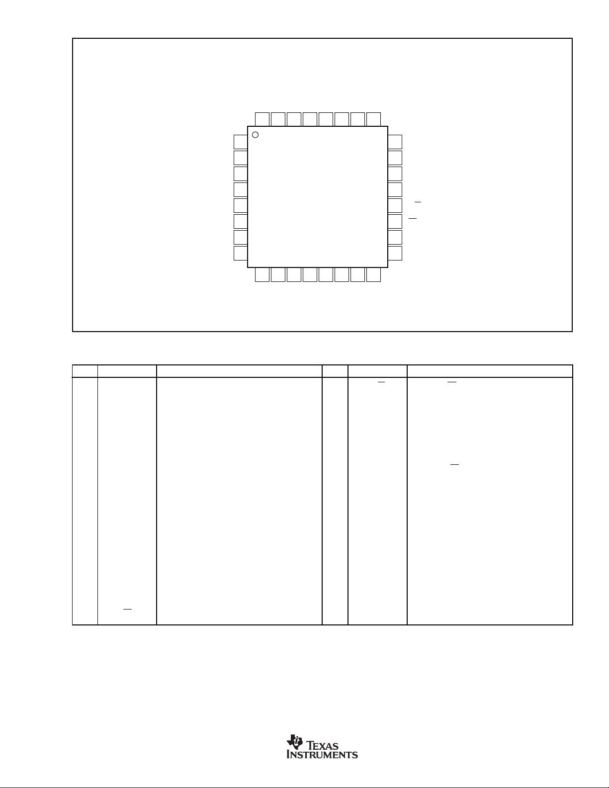
PIN CONFIGURATION
Top View LQFP
A
V
32
OUT
A Sense
L Sense
OUT
REF
V
V
31
30
L
V
REF
29
H
V
28
REF
B Sense
H Sense
REF
OUT
V
V
27
26
B
V
OUT
25
DB15
DB14
DB13
DB12
DB11
DB10
PIN DESCRIPTIONS
PIN NAME DESCRIPTION
1V
CC
2 GND Ground
3 DB15 Data Bit 15, MSB
4 DB14 Data Bit 14
5 DB13 Data Bit 13
6 DB12 Data Bit 12
7 DB11 Data Bit 11
8 DB10 Data Bit 10
9 DB9 Data Bit 9
10 DB8 Data Bit 8
11 DB7 Data Bit 7
12 DB6 Data Bit 6
13 DB5 Data Bit 5
14 DB4 Data Bit 4
15 DB3 Data Bit 3
16 DB2 Data Bit 2
17 DB1 Data Bit 1
18 DB0 Data Bit 0, LSB
19 CS Chip Select, Active LOW
Positive Power Supply
V
GND
1
CC
2
3
4
5
DAC7642
DAC7643
6
7
8
9
10
11
12
13
14
15
DB9
DB8
DB7
DB6
DB5
DB4
DB3
16
DB2
24
23
22
21
20
19
18
17
V
SS
DACSEL
RST
LOADDACS
R/W
CS
DB0
DB1
PIN NAME DESCRIPTION
20 R/W Enabled by CS, Controls Data Read from and Write
to the Input Registers.
21 LOADDACS DAC Output Registers Load Control. Rising edge
triggered. Transfers Data from the Input Registers to
the DAC Registers, Updating the DAC Output.
22 RST Reset, Rising Edge Triggered. DAC7642 resets to
mid-scale, DAC7643 resets to zero. (Resets Both
Input Registers and DAC Registers)
23 DACSEL Enabled by CS. Selects the individual DAC Input
Registers. (LOW Selects Register A, HIGH Selects
Register B)
24 V
25 V
26 V
27 V
OUT
REF
28 V
29 V
30 V
31 V
REF
OUT
32 V
SS
OUT
B Sense DAC B Output Amplifier Inverting Input. Used to
H Sense DAC A and B Reference High Sense Input
REF
OUT
L Sense DAC A and B Reference Low Sense Input
A Sense DAC A Output Amplifier Inverting Input. Used to
OUT
Negative Power Supply
B DAC B Voltage Output
close the feedback loop at the load.
H DAC A and B Reference High Input
L DAC A and B Reference Low Input
close the feedback loop at the load.
A DAC A Output Voltage
DAC7642, DAC7643
SBAS233
www.ti.com
5
Page 6
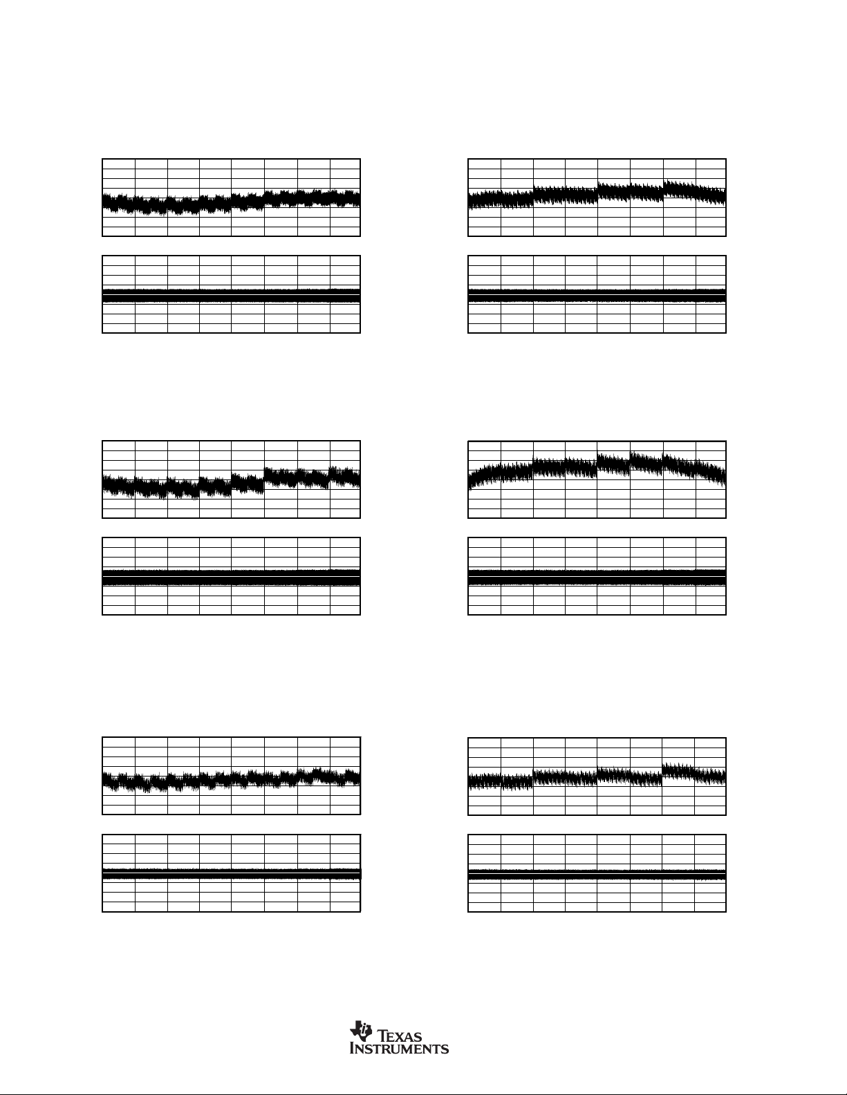
TYPICAL CHARACTERISTICS: VSS = 0V
At TA = +25°C, VCC = +5V, VSS = 0V, V
REFH
= +2.5V, V
= 0V, representative unit, unless otherwise specified.
REFL
+25°C
2.0
1.5
1.0
0.5
–0.5
LE (LSB)DLE (LSB)
–1.0
–1.5
–2.0
2.0
1.5
1.0
0.5
–0.5
–1.0
–1.5
–2.0
+85°C
2.0
1.5
1.0
0.5
–0.5
LE (LSB)DLE (LSB)
–1.0
–1.5
–2.0
2.0
1.5
1.0
0.5
–0.5
–1.0
–1.5
–2.0
DIFFERENTIAL LINEARITY ERROR vs CODE
LINEARITY ERROR AND
(DAC A, +25°C)
0
0
0000H2000H4000H6000H8000
Digital Input Code
LINEARITY ERROR AND
DIFFERENTIAL LINEARITY ERROR vs CODE
(DAC A, +85°C)
0
0
0000H2000H4000H6000H8000
Digital Input Code
DIFFERENTIAL LINEARITY ERROR vs CODE
LINEARITY ERROR AND
(DAC B, +25°C)
2.0
1.5
1.0
0.5
0
–0.5
LE (LSB)DLE (LSB)
–1.0
–1.5
–2.0
2.0
1.5
1.0
0.5
0
–0.5
–1.0
–1.5
A000
H
C000HE000HFFFF
H
H
–2.0
0000H2000H4000H6000H8000
A000
H
C000HE000HFFFF
H
H
Digital Input Code
LINEARITY ERROR AND
DIFFERENTIAL LINEARITY ERROR vs CODE
(DAC B, +85°C)
2.0
1.5
1.0
0.5
0
–0.5
LE (LSB)DLE (LSB)
–1.0
–1.5
–2.0
2.0
1.5
1.0
0.5
0
–0.5
–1.0
–1.5
C000HE000HFFFF
A000
H
H
H
–2.0
0000H2000H4000H6000H8000
C000HE000HFFFF
A000
H
H
H
Digital Input Code
–40°C
2.0
1.5
1.0
0.5
–0.5
LE (LSB)DLE (LSB)
–1.0
–1.5
–2.0
2.0
1.5
1.0
0.5
–0.5
–1.0
–1.5
–2.0
6
DIFFERENTIAL LINEARITY ERROR vs CODE
LINEARITY ERROR AND
(DAC A, –40°C)
0
0
0000H2000H4000H6000H8000
Digital Input Code
DIFFERENTIAL LINEARITY ERROR vs CODE
LINEARITY ERROR AND
(DAC B, –40°C)
2.0
1.5
1.0
0.5
0
–0.5
LE (LSB)DLE (LSB)
–1.0
–1.5
–2.0
2.0
1.5
1.0
0.5
0
–0.5
–1.0
–1.5
C000HE000HFFFF
A000
H
H
H
–2.0
0000H2000H4000H6000H8000
C000HE000HFFFF
A000
H
H
H
Digital Input Code
DAC7642, DAC7643
www.ti.com
SBAS233
Page 7

TYPICAL CHARACTERISTICS: VSS = 0V (Cont.)
3
2
1
0
–1
–2
–3
Temperature (°C)
–40 –15 8510 35 60
POSITIVE FULL-SCALE ERROR vs TEMPERATURE
Positive Full-Scale Error (mV)
DAC A
DAC B
Code (FFFFH)
1.0
0.8
0.6
0.4
0.2
0.0
Digital Input Code
0000H2000H4000H6000H8000HA000HC000HE000HFFFF
H
SUPPLY CURRENT vs DIGITAL INPUT CODE
I
CC
(mA)
All DACs
No Load
At TA = +25°C, VCC = +5V, VSS = 0V, V
NEGATIVE FULL-SCALE ERROR vs TEMPERATURE
3
Code (0040H)
2
1
0
–1
–2
Negative Full-Scale Error (mV)
–3
–40 –15 8510 35 60
Temperature (°C)
V
H CURRENT vs CODE
REF
(all DACs sent to indicated code)
0.30
REFH
= +2.5V, V
DAC A
DAC B
= 0V, representative unit, unless otherwise specified.
REFL
0.00
(all DACs sent to indicated code)
V
L CURRENT vs CODE
REF
0.25
0.20
0.15
Current (mA)
0.10
REF
V
0.05
0.00
0000H2000H4000H6000H8000
SUPPLY CURRENT vs TEMPERATURE
1
Data = FFFFH (all DACs)
No Load
0.8
0.6
(mA)
CC
I
0.4
A000HC000HE000HFFFF
H
Digital Input Code
–0.05
–0.10
–0.15
Current (mA)
–0.20
REF
V
–0.25
–0.30
H
0000H2000H4000H6000H8000
A000HC000HE000HFFFF
H
H
Digital Input Code
0.2
0
–40 –15 10 35 60 85
Temperature (°C)
DAC7642, DAC7643
SBAS233
www.ti.com
7
Page 8
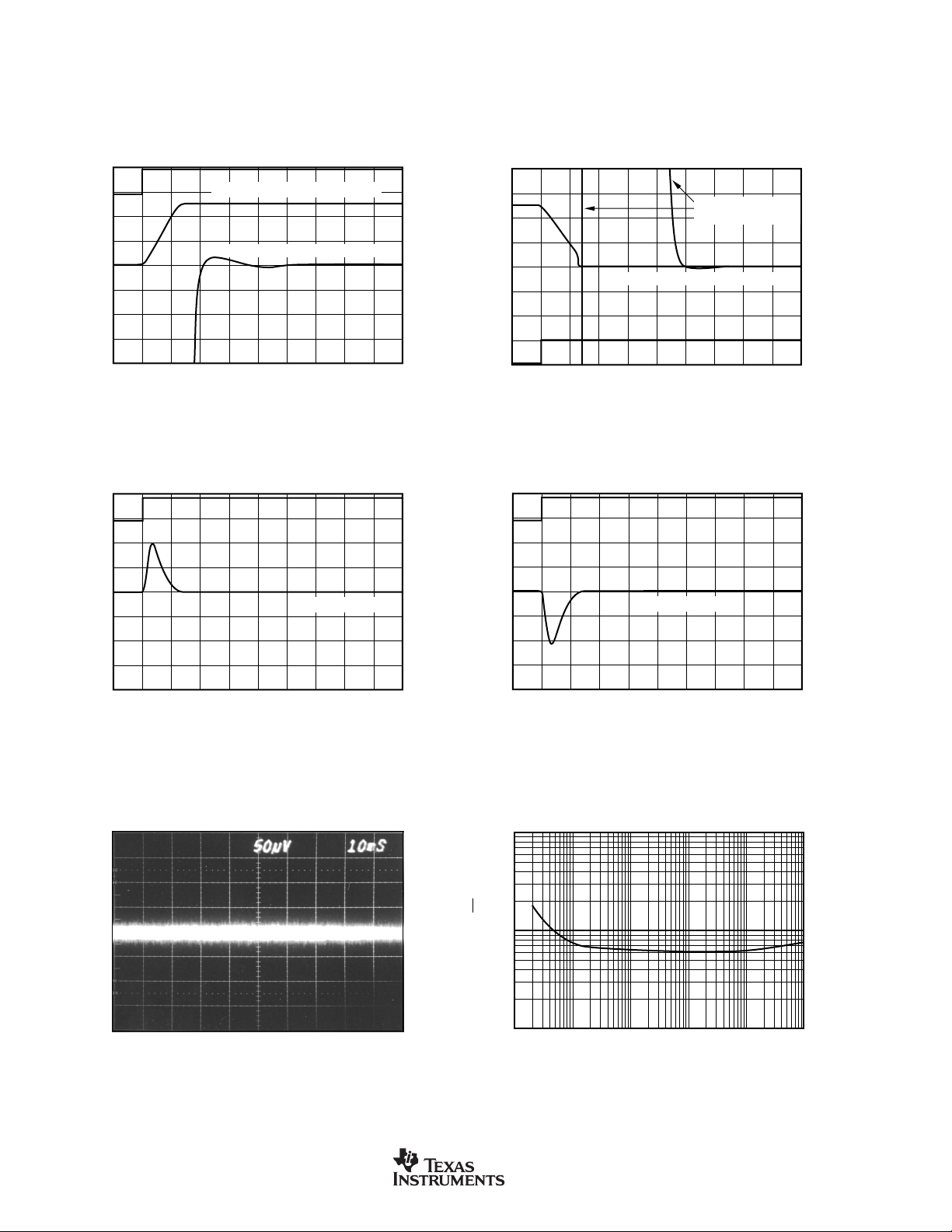
TYPICAL CHARACTERISTICS: VSS = 0V (Cont.)
At TA = +25°C, VCC = +5V, VSS = 0V, V
REFH
= +2.5V, V
= 0V, representative unit, unless otherwise specified.
REFL
OUTPUT VOLTAGE vs SETTLING TIME
Output Voltage
vs MIDSCALE GLITCH PERFORMANCE
(0V to +2.5V)
Large-Signal Settling Time: 1V/div
Small-Signal Settling Time: 500µV/div
Time (2µs/div)
OUTPUT VOLTAGE
+5V
LDAC
0
+5V
LDAC
0
OUTPUT VOLTAGE vs SETTLING TIME
Output Voltage
vs MIDSCALE GLITCH PERFORMANCE
(+2.5V to 2mV)
Small-Signal Settling
Time: 500µV/div
Large-Signal Settling Time: 1V/div
Time (2µs/div)
OUTPUT VOLTAGE
+5V
LDAC
0
+5V
LDAC
0
Output Voltage (20mV/div)
BROADBAND NOISE
Noise Voltage (50µV/div)
Time (1µs/div)
Time (10µs/div)
7FFFH to 8000
H
Output Voltage (20mV/div)
1000
100
Noise (nV/√Hz)
10
OUTPUT NOISE VOLTAGE vs FREQUENCY
10
100
8000H to 7FFF
Time (1µs/div)
1000 10000
Frequency (Hz)
H
100000
1000000
8
www.ti.com
DAC7642, DAC7643
SBAS233
Page 9

TYPICAL CHARACTERISTICS: VSS = 0V (Cont.)
5
4
3
2
1
0
R
LOAD
(kΩ)
0.01
0.1
1 10 100
V
OUT
vs R
LOAD
V
OUT
(V)
Source
Sink
At TA = +25°C, VCC = +5V, VSS = 0V, V
REFH
= +2.5V, V
= 0V, representative unit, unless otherwise specified.
REFL
vs LOGIC INPUT LEVEL FOR DIGITAL INPUTS
LOGIC SUPPLY CURRENT
0.50
Typical of One
Digital Input
0.40
0.30
0.20
0.10
Logic Supply Current (mA)
0.00
0
1
23
Logic Input Level for Digital Inputs (V)
VSS = –5V
At TA = +25°C, VCC = +5V, VSS = –5V, V
+25°C
1.0
0.5
–0.5
–1.0
–1.5
LE (LSB)DLE (LSB)
–2.0
–2.5
–3.0
2.0
1.5
1.0
0.5
–0.5
–1.0
–1.5
–2.0
0
0
DIFFERENTIAL LINEARITY ERROR vs CODE
0000H2000H4000H6000H8000
LINEARITY ERROR AND
(DAC A, +25°C)
Digital Input Code
REFH
H
= +2.5V, V
A000
REFL
C000HE000HFFFF
H
4
5
= –2.5V, representative unit, unless otherwise specified.
DIFFERENTIAL LINEARITY ERROR vs CODE
1.0
0.5
0
–0.5
–1.0
–1.5
LE (LSB)DLE (LSB)
–2.0
–2.5
–3.0
2.0
1.5
1.0
0.5
0
–0.5
–1.0
–1.5
–2.0
H
0000H2000H4000H6000H8000
LINEARITY ERROR AND
(DAC B, +25°C)
A000
H
H
Digital Input Code
C000HE000HFFFF
H
+85°C
LINEARITY ERROR AND
DIFFERENTIAL LINEARITY ERROR vs CODE
1.0
0.5
0
–0.5
–1.0
–1.5
LE (LSB)DLE (LSB)
–2.0
–2.5
–3.0
2.0
1.5
1.0
0.5
0
–0.5
–1.0
–1.5
–2.0
0000H2000H4000H6000H8000
DAC7642, DAC7643
SBAS233
(DAC A, +85°C)
A000
H
Digital Input Code
C000HE000HFFFF
H
H
www.ti.com
DIFFERENTIAL LINEARITY ERROR vs CODE
LINEARITY ERROR AND
1.0
0.5
0
–0.5
–1.0
–1.5
LE (LSB)DLE (LSB)
–2.0
–2.5
–3.0
2.0
1.5
1.0
0.5
0
–0.5
–1.0
–1.5
–2.0
0000H2000H4000H6000H8000
(DAC B, +85°C)
A000
H
Digital Input Code
C000HE000HFFFF
H
H
9
Page 10
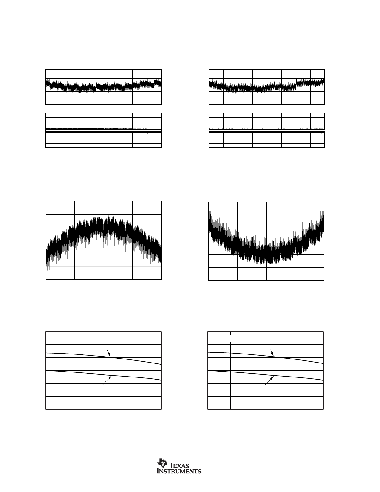
TYPICAL CHARACTERISTICS: VSS = –5V (Cont.)
At TA = +25°C, VCC = +5V, VSS = –5V, V
REFH
= +2.5V, V
= –2.5V, representative unit, unless otherwise specified.
REFL
–40°C
1.0
0.5
–0.5
–1.0
–1.5
LE (LSB)DLE (LSB)
–2.0
–2.5
–3.0
2.0
1.5
1.0
0.5
–0.5
–1.0
–1.5
–2.0
0.6
0.5
0.4
DIFFERENTIAL LINEARITY ERROR vs CODE
LINEARITY ERROR AND
(DAC A, –40°C)
0
0
0000H2000H4000H6000H8000
H
Digital Input Code
V
H CURRENT vs CODE
REF
(all DACs sent to indicated code)
C000HE000HFFFF
A000
H
DIFFERENTIAL LINEARITY ERROR vs CODE
LINEARITY ERROR AND
(DAC B, –40°C)
1.0
0.5
0
–0.5
–1.0
–1.5
LE (LSB)DLE (LSB)
–2.0
–2.5
–3.0
2.0
1.5
1.0
0.5
0
–0.5
–1.0
–1.5
–2.0
H
0000H2000H4000H6000H8000
H
C000HE000HFFFF
A000
H
H
Digital Input Code
V
L CURRENT vs CODE
REF
(all DACs sent to indicated code)
0.0
–0.1
–0.2
0.3
Current (mA)
0.2
REF
V
0.1
0.0
0000H2000H4000H6000H8000
A000HC000HE000HFFFF
H
Digital Input Code
BIPOLAR ZERO ERROR vs TEMPERATURE
3
Code (8000H)
2
DAC A
1
0
–1
Bipolar Zero Error (mV)
DAC B
–2
–3
–40 –15 8510 35 60
Temperature (°C)
–0.3
Current (mA)
–0.4
REF
V
–0.5
–0.6
H
0000H2000H4000H6000H8000
A000HC000HE000HFFFF
H
H
Digital Input Code
POSITIVE FULL-SCALE ERROR vs TEMPERATURE
3
Code (FFFFH)
2
DAC A
1
0
–1
DAC B
–2
Positive Full-Scale Error (mV)
–3
–40 –15 8510 35 60
Temperature (°C)
10
www.ti.com
DAC7642, DAC7643
SBAS233
Page 11

TYPICAL CHARACTERISTICS: VSS = –5V (Cont.)
Time (2µs/div)
OUTPUT VOLTAGE vs SETTLING TIME
(+2.5V to –2.5V)
Output Voltage
+5V
LDAC
0
Large-Signal Settling Time: 2V/div
Small-Signal Settling Time:
500µV/div
1.00
0.75
0.50
0.25
0.00
–0.25
–0.50
–0.75
–1.00
SUPPLY CURRENT vs DIGITAL INPUT CODE
Supply Current (mA)
0000H2000H4000
H
I
CC
I
SS
6000H8000
H
Digital Input Code
A000HC000HE000HFFFF
H
No Load
At TA = +25°C, VCC = +5V, VSS = –5V, V
NEGATIVE FULL-SCALE ERROR vs TEMPERATURE
3
Code (0000H)
2
1
0
–1
–2
Negative Full-Scale Error (mV)
DAC B
–3
–40 –15 8510 35 60
Temperature (°C)
V
5
OUT
4
3
2
1
(V)
0
OUT
V
–1
–2
–3
–4
–5
0.01
0.1
R
REFH
= +2.5V, V
= –2.5V, representative unit, unless otherwise specified.
REFL
DAC A
vs R
LOAD
Source
Sink
1 10 100
(kΩ)
LOAD
1
SUPPLY CURRENT vs TEMPERATURE
0.5
0
–0.5
Supply Current (mA)
–1
Data = FFFFH (all DACs)
–1.5
No Load
–40 –15 10 35 60 85
Temperature (°C)
I
CC
I
SS
OUTPUT VOLTAGE vs SETTLING TIME
Output Voltage
DAC7642, DAC7643
SBAS233
(–2.5V to +2.5V)
Large-Signal Settling Time: 2V/div
Small-Signal Settling Time: 500µV/div
Time (2µs/div)
+5V
LDAC
0
www.ti.com
11
Page 12

TYPICAL CHARACTERISTICS: VSS = –5V (Cont.)
At TA = +25°C, VCC = +5V, VSS = –5V, V
REFH
= +2.5V, V
= –2.5V, representative unit, unless otherwise specified.
REFL
vs MIDSCALE GLITCH PERFORMANCE
Output Voltage (50mV/div)
OUTPUT VOLTAGE
Time (1µs/div)
7FFFH to 8000
H
+5V
LDAC
0
THEORY OF OPERATION
The DAC7642 and DAC7643 are dual channel, voltage
output, 16-bit DACs. The architecture is an R-2R ladder
configuration with the three MSB’s segmented followed by an
operational amplifier that serves as a buffer. Each DAC has
its own R-2R ladder network, segmented MSBs, and output
op amp, as shown in Figure 1. The minimum voltage output
(zero-scale) and maximum voltage output (full-scale) are set
vs MIDSCALE GLITCH PERFORMANCE
Output Voltage (50mV/div)
by the external voltage references V
OUTPUT VOLTAGE
Time (1µs/div)
L and V
REF
8000H to 7FFF
H, respec-
REF
H
+5V
LDAC
0
tively. The digital input is a 16-bit parallel word and the DAC
input registers offer a readback capability. The converters
can be powered from either a single +5V supply or a dual
±5V supply. Each device offers a reset function which immediately sets all DAC output voltages, DAC registers and Input
registers to mid-scale, code 8000
scale, code 0000
(DAC7643). See Figures 2 and 3 for the
H
(DAC7642), or to zero-
H
basic configurations of the DAC7642 and DAC7643.
R
2R2R 2R 2R 2R 2R 2R 2R
2R
FIGURE 1. DAC7642 and DAC7643 Architecture.
V
V
V
V
REF
REF
REF
REF
R
F
H
H Sense
L
L Sense
V
Sense
OUT
V
OUT
12
www.ti.com
DAC7642, DAC7643
SBAS233
Page 13
REFL
+2.5V
V
REFH
V
REFL
DAC7642
DAC7643
27 26 25
V
Sense
V
REFH
Sense
0V to +2.5V
OUTB
V
OUTB
DACSEL
LDAC
+5V
1µF
DATA BUS
0.1µF
0V to +2.5V
1
V
CC
2
GND
3
DB15
4
DB14
5
DB13
6
DB12
7
DB11
8
DB10
V
OUTA
32
V
Sense
OUTA
31 30 29 28
V
Sense
DB9 DB8 DB7 DB6 DB5 DB4 DB3 DB2
9 10 11 12 13 14 15 16
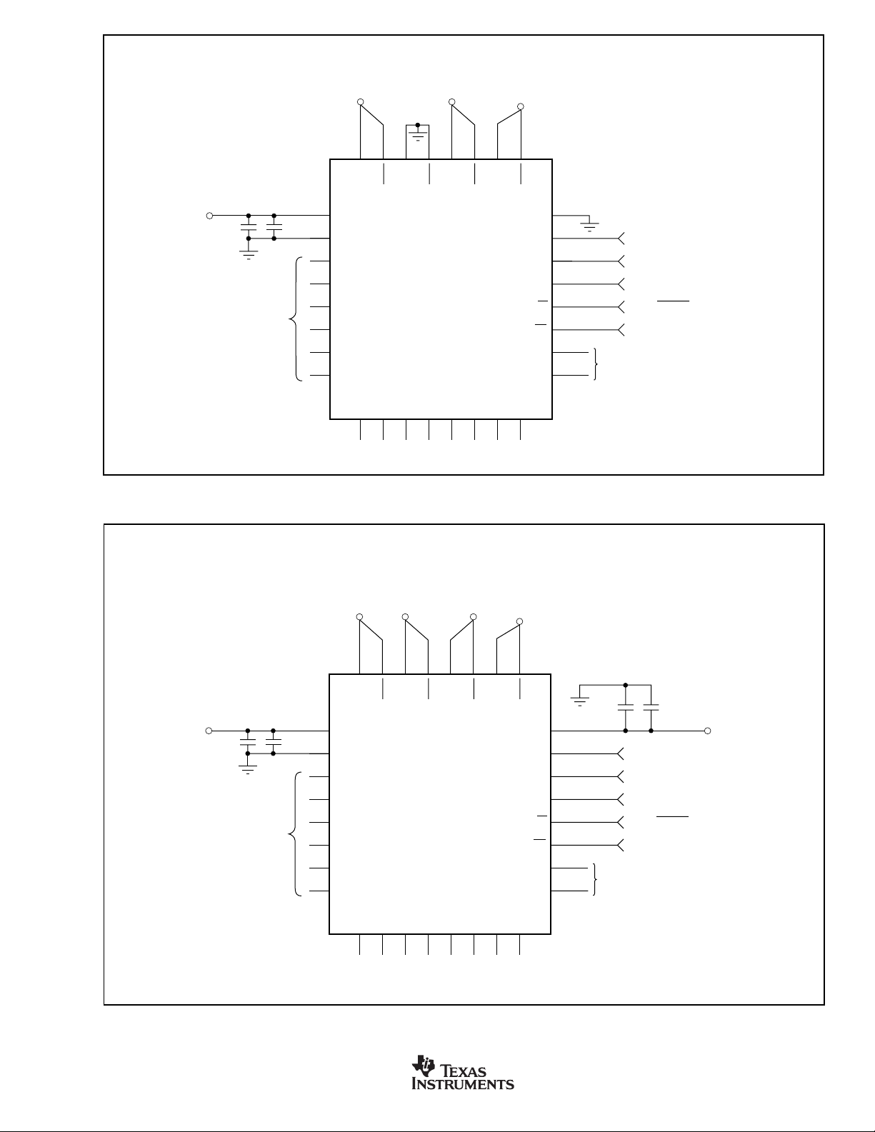
FIGURE 2. Basic Single-Supply Operation of the DAC7642 and DAC7643.
V
RST
R/W
CS
DB0
DB1
24
SS
23
22
21
20
19
SELECT DAC CHANNEL
RESET DAC REGISTERS
LOAD DAC REGISTERS
READ/WRITE
CHIP SELECT
18
17
DATA BUS
+5V
1µF
DATA BUS
0.1µF
–2.5V to
+2.5V
V
1
V
CC
2
GND
3
DB15
4
DB14
5
DB13
6
DB12
7
DB11
8
DB10
–2.5V
32 31 30 29
V
OUTA
V
OUTA
Sense
REFL
Sense
V
REFH
V
REFL
DAC7642
DAC7643
28
DB9 DB8 DB7 DB6 DB5 DB4 DB3 DB2
9 10 11 12 13 14 15 16
+2.5V
27 26 25
Sense
V
REFH
Sense
V
OUTB
–2.5V to
+2.5V
V
OUTB
DACSEL
LDAC
V
RST
R/W
CS
DB0
DB1
24
SS
23
22
21
20
19
SELECT DAC CHANNEL
RESET DAC REGISTERS
LOAD DAC REGISTERS
READ/WRITE
CHIP SELECT
–5V
18
0.1µF1µF
17
DATA BUS
FIGURE 3. Basic Dual-Supply Operation of the DAC7642 and DAC7643.
DAC7642, DAC7643
SBAS233
www.ti.com
13
Page 14

ANALOG OUTPUTS
When VSS = –5V (dual-supply operation), the output amplifier
can swing to within 2.25V of the supply rails over the –40°C
to +85°C temperature range. When V
operation), and with R
also connected to ground, the
LOAD
= 0V (single-supply
SS
output can swing to ground. Care must also be taken when
measuring the zero-scale error when V
= 0V. Since the
SS
DAC output cannot swing below ground, the output voltage
may not change for the first few digital input codes (0000
0001
, 0002H, etc.) if the output amplifier has a negative
H
offset. At the negative limit of –2mV, the first specified output
starts at code 0040
.
H
Due to the high accuracy of these DACs, system design
problems such as grounding and contact resistance become
very important. A 16-bit converter with a 2.5V full-scale range
has a 1LSB value of 38µV. With a load current of 1mA, a series
wiring and connector resistance of only 40mΩ (R
) will cause
W2
a voltage drop of 40µV, as shown in Figure 4. To understand
what this means in terms of a system layout, the resistivity of
a typical 1 ounce copper-clad printed circuit board is 1/2 mΩ
per square. For a 1mA load, a 10 milli-inch wide printed circuit
conductor 600 milli-inches long will result in a voltage drop of
30µV.
The DAC7642 and DAC7643 offer a force and sense output
configuration for the high open-loop gain output amplifiers.
This feature allows the loop around the output amplifier to be
closed at the load (shown in Figure 4), thus ensuring an
accurate output voltage.
REFERENCE INPUTS
The reference inputs, V
between V
+ 2.5V and V
SS
at least 1.25V greater than V
each DAC is equal to V
(essentially, the offset of the output op amp). The maximum
output is equal to V
L and V
REF
– 2.5V provided that V
CC
REF
REFL
H plus a similar offset voltage. Note
REF
H, can be any voltage
REF
L. The minimum output of
plus a small offset voltage
REF
H is
R
W2
32
V
A
OUT
V
A Sense
OUT
L Sense
V
REF
DAC7642
DAC7643
,
H
V
V
REF
OUT
H Sense
B Sense
31
30
29
V
L
REF
28
V
H
REF
27
26
25
B
V
OUT
FIGURE 4. Analog Output Closed-Loop Configuration. R
R
W1
R
W1
R
W2
V
OUT
+V
+2.5V
V
OUT
W
represents wiring resistances.
that VSS (the negative power supply) must either be connected to ground or must be in the range of –4.75V to
–5.25V. The voltage on V
the converter. If V
is not in one of these two configurations,
SS
sets several bias points within
SS
the bias values may be in error and proper operation of the
device may be affected.
The current into the V
H input and out of V
REF
L depends
REF
on the DAC output voltages and can vary from a few
microamps to approximately 0.5mA. The reference input
appears as a varying load to the reference. If the references
applied can sink or source the required current, a reference
buffer is not required. The DAC7642 and DAC7643 feature
reference drive and sense connections such that the internal
errors caused by the changing reference current and the
circuit impedances can be minimized. Figures 5 through 13
show different reference configurations and the effect on the
linearity and differential linearity.
+V
OPA2234
–V
+V
–V
DAC7642
DAC7643
V
V
V
V
OUT
REF
REF
OUT
V
OUT
A Sense
L Sense
V
REF
V
REF
H Sense
B Sense
V
OUT
32
A
31
30
29
L
28
H
27
26
25
B
V
OUT
1000pF
1000pF
V
OUT
100Ω
2200pF
100Ω
2200pF
FIGURE 5. Dual Supply Configuration-Buffered References, Used for Dual-Supply Characteristic Curves.
14
www.ti.com
DAC7642, DAC7643
–2.5V
+2.5V
SBAS233
Page 15

+V
2.0
1.5
1.0
0.5
0
–0.5
–1.0
–1.5
–2.0
2.0
1.5
1.0
0.5
0
–0.5
–1.0
–1.5
–2.0
LE (LSB)DLE (LSB)
LINEARITY ERROR AND
DIFFERENTIAL LINEARITY ERROR vs CODE
(DAC A, +25°C)
0000H2000H4000H6000H8000
H
Digital Input Code
A000
H
C000HE000HFFFF
H
32
A
OUT
31
30
29
V
L
REF
28
H
REF
27
26
25
B
OUT
DAC7642
DAC7643
V
V
V
V
OUT
REF
REF
OUT
V
A Sense
L Sense
V
H Sense
B Sense
V
FIGURE 6. Single-Supply Buffered Reference with V
DIFFERENTIAL LINEARITY ERROR vs CODE
2.0
1.5
1.0
0.5
0
–0.5
LE (LSB)DLE (LSB)
–1.0
–1.5
–2.0
2.0
1.5
1.0
0.5
0
–0.5
–1.0
–1.5
–2.0
0000H2000H4000H6000H8000
LINEARITY ERROR AND
(DAC A, +25°C)
A000HC000HE000HFFFF
H
Digital Input Code
V
OUT
1000pF
1000pF
V
OUT
L of 50mV.
REF
H
100Ω
2200pF
100Ω
2200pF
OPA2350
2kΩ
+0.050V
98kΩ
+V
+2.5V
FIGURE 7. Integral Linearity and Differential Linearity Error
FIGURE 9. Single-Supply Buffered Reference with V
DAC7642, DAC7643
Curves for Figure 6.
DAC7642
DAC7643
SBAS233
V
V
A Sense
OUT
V
L Sense
REF
V
V
V
H Sense
REF
V
B Sense
OUT
V
OUT
REF
REF
OUT
FIGURE 8. Integral Linearity and Differential Linearity Error
Curves for Figure 9.
+V
+V
32
A
31
30
29
L
28
H
27
26
25
B
V
OUT
100Ω
1000pF
1000pF
V
OUT
L = +1.25V and V
REF
www.ti.com
2200pF
100Ω
2200pF
REF
OPA2350
+1.25V
+V
+2.5V
H = +2.5V.
15
Page 16

DAC7642
DAC7643
V
V
V
V
OUT
REF
H Sense
REF
OUT
V
OUT
A Sense
L Sense
V
REF
V
REF
B Sense
V
OUT
32
A
31
30
29
L
28
H
27
26
25
B
V
1000pF
V
OUT
OUT
100Ω
2200pF
+V
OPA2350
+V
+2.5V
FIGURE 10. Single-Supply Buffered V
DIFFERENTIAL LINEARITY ERROR vs CODE
2.0
1.5
1.0
0.5
0
–0.5
LE (LSB)DLE (LSB)
–1.0
–1.5
–2.0
2.0
1.5
1.0
0.5
0
–0.5
–1.0
–1.5
–2.0
0000H2000H4000H6000H8000
LINEARITY ERROR AND
(DAC A, +25°C)
H
Digital Input Code
H.
REF
A000HC000HE000HFFFF
H
FIGURE 11. Linearity and Differential Linearity Error Curves
for Figure 10.
V
OUT
+V
+2.5V
V
OUT
DAC7642
DAC7643
V
V
V
V
OUT
REF
REF
OUT
V
OUT
A Sense
L Sense
V
REF
V
REF
H Sense
B Sense
V
OUT
32
A
31
30
29
L
28
H
27
26
25
B
FIGURE 12. Low-Cost Single-Supply Configuration.
DIFFERENTIAL LINEARITY ERROR vs CODE
2.0
1.5
1.0
0.5
0
–0.5
LE (LSB)DLE (LSB)
–1.0
–1.5
–2.0
2.0
1.5
1.0
0.5
0
–0.5
–1.0
–1.5
–2.0
0000H2000H4000H6000H8000
LINEARITY ERROR AND
(DAC A, +25°C)
A000HC000HE000HFFFF
H
Digital Input Code
H
FIGURE 13. Linearity and Differential Linearity Error Curves
for Figure 12.
DIGITAL INTERFACE
See Table I for the basic control logic of the DAC7642 and
DAC7643. Note that each internal register is edge triggered
and not level triggered. When the LOADDACS signal is
transitioned from LOW to HIGH, the digital word existing in
the input register is latched into the DAC register. The first
set of registers (the input registers) are triggered via the
DACSEL, R/W, and CS inputs. Only one of these registers
can be transparent at any given time.
The double-buffered architecture is designed mainly so each
DAC input register can be written to at any time without
affecting the DAC outputs. All DAC voltages are updated
simultaneously by the rising edge of LOADDACS. It also
allows multiple devices to be updated simultaneously by
sharing the LOADDACS control from the host with each
device.
16
www.ti.com
DAC7642, DAC7643
SBAS233
Page 17

DACSEL R/W CS RST LOADDACS REGISTER REGISTER MODE DAC
INPUT DAC
L L L L, H X Write Hold Write Input A
H L L L, H X Write Hold Write Input B
L H L L, H X Read Hold Read Input A
H H L L, H X Read Hold Read Input B
X X H L, H ↑ Hold Write Update All
X X H L, H L, H Hold Hold Hold All
XXX↑ L, H Reset Reset Reset All
TABLE I. DAC7642 and DAC7643 Logic Truth Table.
DIGITAL TIMING
Figure 14 and Table II provide detailed timing for the digital
interface of the DAC7642 and DAC7643.
DIGITAL INPUT CODING
The DAC7642 and DAC7643 input data is in Straight Binary
format. The output voltage is given by Equation 1:
t
CS
R/W
DACSEL
Data Out
t
RDS
Data Read Timing
RCS
t
RDH
Data Valid
t
CSD
t
AH
t
DZ
t
RSS
RST
+FS
t
AS
DACSEL
LOADDACS
Data In
t
RSH
VVL
=+
OUT
(
REF
REF REF
)
,65 536
–•
VHVLN
where N is the digital input code. This equation does not
include the effects of offset (zero-scale) or gain (full-scale)
errors.
t
WCS
t
WS
t
AS
t
LWD
Data Write Timing
t
S
t
WH
t
AH
t
t
LS
LH
t
LX
±0.003% of FSR
t
DH
t
S
Error Band
±0.003% of FSR
Error Band
R/W
V
CS
OUT
t
DS
(1)
V
OUT
V
OUT
FIGURE 14. Digital Input and Output Timing.
DAC7642, DAC7643
SBAS233
–FS
+FS
–FS
(DAC7643)
(DAC7642)
www.ti.com
Zero-Scale
Midscale
17
Page 18

SYMBOL DESCRIPTION MIN TYP MAX UNITS
t
t
t
RDH
t
t
WCS
t
t
t
t
t
t
LWD
t
t
RCS
RDS
t
DZ
CSD
WS
WH
t
AS
AH
t
LS
t
LH
t
LX
DS
DH
RSS
RSH
t
CS HIGH to Data Bus in High Impedance 10 100 ns
S
CS LOW for Read 150 ns
R/W HIGH to CS LOW 10 ns
R/W HIGH after CS HIGH 10 ns
CS LOW to Data Bus Valid 100 150 ns
CS LOW for Write 40 ns
R/W LOW to CS LOW 0 ns
R/W LOW after CS HIGH 10 ns
DACSEL Valid to CS LOW 0 ns
DACSEL Valid after CS HIGH 10 ns
CS LOW to LOADDACS HIGH 30 ns
CS LOW after LOADDACS HIGH 100 ns
LOADDACS HIGH 100 ns
Data Valid to CS LOW 0 ns
Data Valid after CS HIGH 10 ns
LOADDACS LOW 100 ns
RESET LOW 10 ns
RESET HIGH 10 ns
Settling Time 10 µs
TABLE II. Timing Specifications (TA = –40°C to +85°C).
DIGITALLY-PROGRAMMABLE
CURRENT SOURCE
The DAC7642 and DAC7643 offer a unique set of features
that allows a wide range of flexibility in designing applications
circuits, such as programmable current sources. The
DAC7642 and DAC7643 offer both a differential reference
input, as well as an open-loop configuration around the
output amplifier. The open-loop configuration around the
output amplifier allows a transistor to be placed within the
loop to implement a digitally-programmable, unidirectional
current source. The availability of a differential reference also
allows programmability for both the full-scale and zero-scale
currents. The output current is calculated as:
I
OUT
VHVL
–
REF REF
=
R
SENSE
VLR
+
(
REF
DAC7642
DAC7643
SENSE
N Value
•
)
V
OUT
V
REF
V
REF
V
OUT
H Sense
,/65 536
V
OUT
A Sense
L Sense
V
REF
V
REF
B Sense
V
OUT
32
A
31
30
29
L
28
H
27
26
25
B
(2)
1000pF
1000pF
Figure 15 shows a DAC7642 and DAC7643 in a 4-20mA
current output configuration. The output current can be
determined by Equation 3:
(3)
I
OUT
V V N Value V
25 05
. – .
=
ΩΩ
125 65 536
•
.
05
125
+
,
At full-scale, the output current is 16mA plus the 4mA for the
zero current. At zero scale the output current is the offset
current of 4mA (0.5V/125Ω).
I
OUT
V
PROGRAMMED
125Ω
2200pF
100Ω
100Ω
2200pF
I
OUT
+V
OPA2350
20kΩ
80kΩ
+V
+2.5V
FIGURE 15. 4-20mA Digitally Controlled Current Source.
18
V
125Ω
www.ti.com
PROGRAMMED
DAC7642, DAC7643
SBAS233
Page 19

PACKAGE DRAWING
MTQF002B – JANUARY 1995 – REVISED MAY 2000
VF (S-PQFP-G32) PLASTIC QUAD FLATPACK
4040172/D 04/00
Gage Plane
Seating Plane
1,60 MAX
1,45
1,35
8,80
9,20
SQ
0,05 MIN
0,45
0,75
0,25
0,13 NOM
5,60 TYP
1
32
7,20
6,80
24
25
SQ
8
9
17
16
0,25
0,45
0,10
0°–7°
M
0,20
0,80
NOTES: A. All linear dimensions are in millimeters.
B. This drawing is subject to change without notice.
DAC7642, DAC7643
SBAS233
www.ti.com
19
Page 20

IMPORTANT NOTICE
Texas Instruments Incorporated and its subsidiaries (TI) reserve the right to make corrections, modifications,
enhancements, improvements, and other changes to its products and services at any time and to discontinue
any product or service without notice. Customers should obtain the latest relevant information before placing
orders and should verify that such information is current and complete. All products are sold subject to TI’s terms
and conditions of sale supplied at the time of order acknowledgment.
TI warrants performance of its hardware products to the specifications applicable at the time of sale in
accordance with TI’s standard warranty . Testing and other quality control techniques are used to the extent TI
deems necessary to support this warranty . Except where mandated by government requirements, testing of all
parameters of each product is not necessarily performed.
TI assumes no liability for applications assistance or customer product design. Customers are responsible for
their products and applications using TI components. T o minimize the risks associated with customer products
and applications, customers should provide adequate design and operating safeguards.
TI does not warrant or represent that any license, either express or implied, is granted under any TI patent right,
copyright, mask work right, or other TI intellectual property right relating to any combination, machine, or process
in which TI products or services are used. Information published by TI regarding third-party products or services
does not constitute a license from TI to use such products or services or a warranty or endorsement thereof.
Use of such information may require a license from a third party under the patents or other intellectual property
of the third party , or a license from TI under the patents or other intellectual property of TI.
Reproduction of information in TI data books or data sheets is permissible only if reproduction is without
alteration and is accompanied by all associated warranties, conditions, limitations, and notices. Reproduction
of this information with alteration is an unfair and deceptive business practice. TI is not responsible or liable for
such altered documentation.
Resale of TI products or services with statements different from or beyond the parameters stated by TI for that
product or service voids all express and any implied warranties for the associated TI product or service and
is an unfair and deceptive business practice. TI is not responsible or liable for any such statements.
Following are URLs where you can obtain information on other Texas Instruments products and application
solutions:
Products Applications
Amplifiers amplifier.ti.com Audio www.ti.com/audio
Data Converters dataconverter.ti.com Automotive www.ti.com/automotive
DSP dsp.ti.com Broadband www.ti.com/broadband
Interface interface.ti.com Digital Control www.ti.com/digitalcontrol
Logic logic.ti.com Military www.ti.com/military
Power Mgmt power.ti.com Optical Networking www.ti.com/opticalnetwork
Microcontrollers microcontroller.ti.com Security www.ti.com/security
Telephony www.ti.com/telephony
Video & Imaging www.ti.com/video
Wireless www.ti.com/wireless
Mailing Address: T exas Instruments
Post Office Box 655303 Dallas, Texas 75265
Copyright 2003, Texas Instruments Incorporated
 Loading...