

Page 1
User's Guide
SBOU096A–November 2010–Revised January 2011
DAC31x2EVM
This document is a user's guide for the DAC31x2EVM, an evaluation fixture for the DAC3152 and
DAC3162 (DAC31x2) series of dual-channel, 10-/12-bit, 500-MSPS digital-to-analog converters (DACs).
The DAC31x2EVM includes the TRF3703-33 quadrature modulator to facilitate measuring the output
signals at a desired RF frequency. The EVM also includes the CDCP1803 clock buffer that distributes the
clocks to the DAC, as well as a pattern generator. This EVM is ideally suited for mating with the TSW3100
pattern generation card for evaluating QAM, WCDMA, LTE, or other high-performance modulation
schemes. For more information about the DAC31x2 family, see the product data sheet (available for
download at www.ti.com).
Throughout this document, the acronym EVM and the phrases evaluation module and evaluation fixture
are synonymous with the DAC31x2EVM.
Contents
1 Introduction .................................................................................................................. 2
2 Testing and Configuration ................................................................................................. 3
List of Figures
1 DAC31x2EVM Block Diagram............................................................................................. 2
2 DAC31x2EVM Test Setup ................................................................................................. 3
3 TSW3100 CommsSignalPattern (WCDMA) Programming GUI ...................................................... 4
4 DAC3162EVM and TRF3703-33 WCDMA Output ..................................................................... 5
5 DAC3162EVM Transformer-Coupled Output at 30 MHz IF ........................................................... 6
All trademarks are the property of their respective owners.
SBOU096A–November 2010–Revised January 2011 DAC31x2EVM
Submit Documentation Feedback
1
© 2010–2011, Texas Instruments Incorporated
Page 2
+
J2
J9
Optional DAC
Output
+
J3
Optional DAC
Output
J11
J10
RF
LO
TRF3703-33
DAC31x2
A
B
Y0
Y1
DAC_CLK
(LVPECL,
ac-coupled)
DATA
Data_CLK
(LVDS,
dc-coupled)
IN
External CLK Input:
0.5 V Single-ended
500 MSPS Max
(LVPECL, ac-coupled)
RMS
!
!
FPGA CLK:
TSW3100
LVPECL, dc-coupled)
!
(
CDCP1803
PowerSupply
Circuits
5 V GND
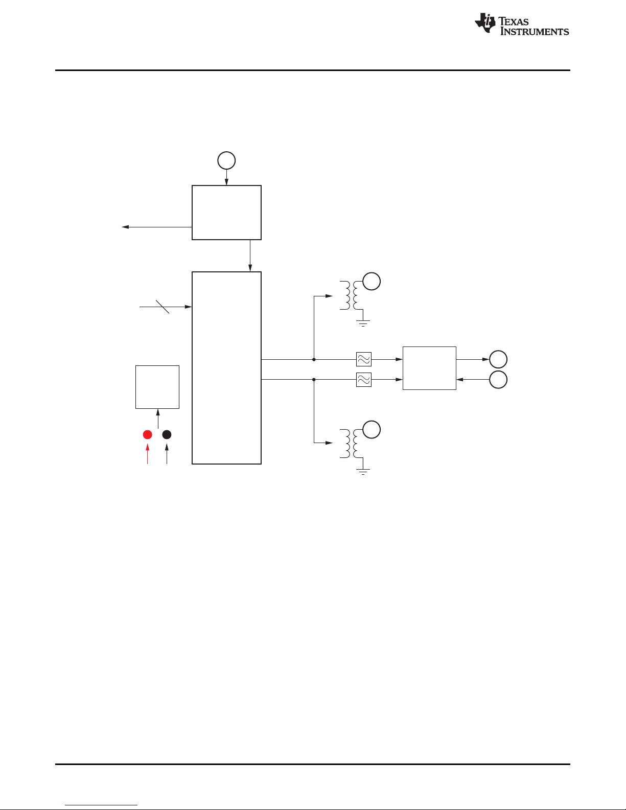
Introduction
1 Introduction
1.1 Block Diagram
Figure 1 shows the DAC31x2EVM block diagram.
www.ti.com
1.2 Software Control
No software is required to use the DAC31x2EVM.
2
DAC31x2EVM SBOU096A–November 2010–Revised January 2011
Figure 1. DAC31x2EVM Block Diagram
© 2010–2011, Texas Instruments Incorporated
Submit Documentation Feedback
Page 3
DAC31x2
J13
J12
J10
J11
J9
J13
J9
TSW3100
Ethernet
PC
+5 V
+5 V/GND
PSA
LO Source
CLK Source
www.ti.com
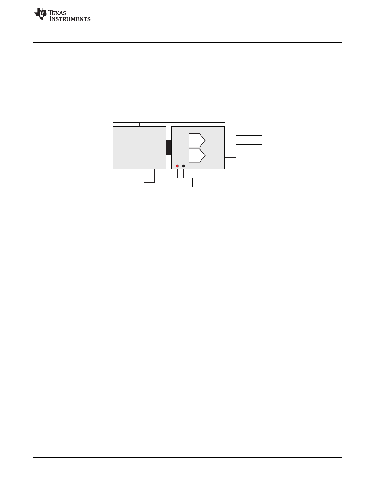
2 Testing and Configuration
This section outlines the basic procedure for testing the DAC31x2EVM.
2.1 Test Set-Up
Figure 2 illustrates the test configuration for general testing of the DAC31x2 with the TSW3100 pattern
generation card.
Testing and Configuration
Figure 2. DAC31x2EVM Test Setup
2.2 Test Set-Up Connections
Follow these procedures to properly connect the DAC31x2EVM and the TSW3100 pattern generator.
TSW3100 Pattern Generator:
• Connect a 5-V power supply to J9, the 5V_IN jack of the TSW3100EVM.
• Connect the PC Ethernet port to J13, the Ethernet port of the TSW3100. The cable should be a
standard crossover Cat5e Ethernet cable.
DAC31x2EVM:
• Connect the J5 connector of DAC31x2EVM to connector J74 of the TSW3100EVM.
• Connect 5 V and Ground to connectors J12 and J13 respectively.
• Provide a 0.5-V
• Provide a 7-dBm, 350-MHz to 4-GHz local oscillator (LO) source at port J10 of the DAC31x2EVM. This
input provides the LO source to the TRF3703-33 modulators.
• Connect the RF output port of (J11) to the spectrum analyzer.
DAC31x2EVM Jumpers:
Power distribution to the DAC31x2 and CDCP1803 devices on the EVM can be achieved through
low-dropout regulators (LDOs) or dc-dc converters. Jumpers JP24, JP25, JP26, and JP27 allow the
user to choose one of the power schemes from these two available options. The default setting of
these jumpers is shown; these settings use power management for the ICs through dc-dc switchers.
• JP24 on pin {1,2}
• JP25 on pin {1,2}
• JP26 on pin {1,2}
• JP27 on pin {1,2}
Jumper JP4 supplies power to the TRF3703-33 modulator. This jumper must be installed in order to use
the modulator.
, 500-MHz (max) clock at J9, the CLOCK IN SMA port of the DAC31x2EVM.
RMS
SBOU096A–November 2010–Revised January 2011 DAC31x2EVM
Submit Documentation Feedback
3
© 2010–2011, Texas Instruments Incorporated
Page 4

Testing and Configuration
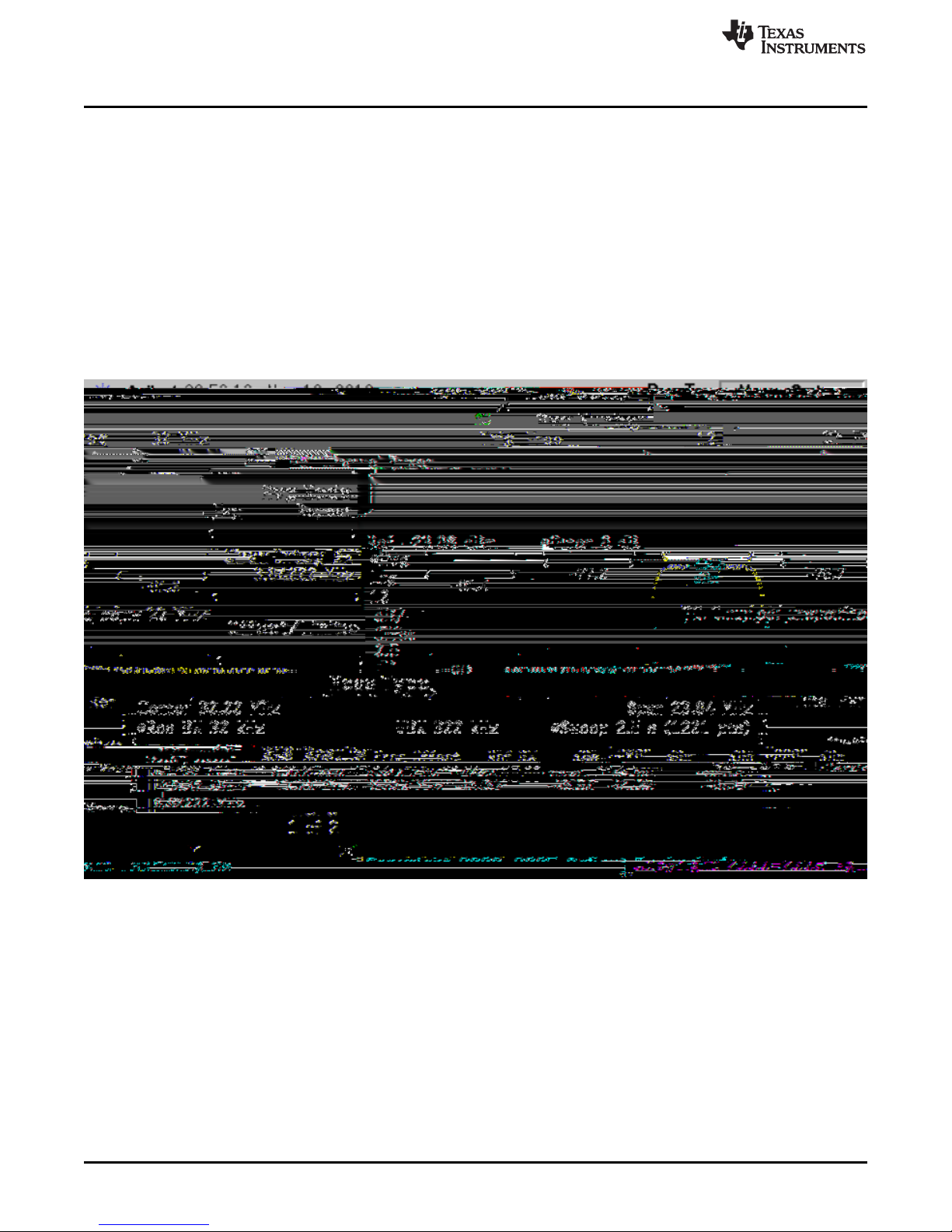
2.3 TSW3100 Quick-Start Operation
Refer to the TSW3100 User’s Guide for a more detailed discussion of how to set up and operate the
TSW3100. This user guide presumes that the TSW3100 software is installed and functioning properly.
CommsSignalPattern Setup from Default Configuration (WCDMA):
Step 1. Change the interpolation value to DAC Clock Rate / 3.84 (that is, 491.52/3.84 = 128).
Step 2. Enter the desired offset frequency (for example, 30 MHz) for each desired carrier.
Step 3. Select the LVDS Output button.
Step 4. Select the Offset Binary option.
Step 5. Check the LOAD and Run box.
Step 6. Press the green Create button.
Figure 3 shows a screenshot of the properly configured TSW3100 software interface.
www.ti.com
Figure 3. TSW3100 CommsSignalPattern (WCDMA) Programming GUI
4
DAC31x2EVM SBOU096A–November 2010–Revised January 2011
© 2010–2011, Texas Instruments Incorporated
Submit Documentation Feedback
Page 5

www.ti.com
2.4 DAC31x2EVM Configuration for Modulator Output
Follow these steps to set up the DAC31x2EVM and perform a spectrum analysis.
Step 1. Set the clock input to 491.52 MHz at 0.5 V
Step 2. Supply the LO source of 900 MHz (7 dBm) at the J10 SMA connector of the DAC31x2EVM.
Step 3. Turn on power to the board at J12/J13.
Step 4. Verify the spectrum using the Spectrum Analyzer at the RF output of the DAC31x2EVM
(J11).
A typical WCDMA output from a wave analyzer is shown in Figure 4.
RMS
Testing and Configuration
at the J9 SMA connector of the DAC31x2EVM.
Figure 4. DAC3162EVM and TRF3703-33 WCDMA Output
SBOU096A–November 2010–Revised January 2011 DAC31x2EVM
Submit Documentation Feedback
5
© 2010–2011, Texas Instruments Incorporated
Page 6
Testing and Configuration
2.5 DAC31x2EVM Configuration for DAC Output
Follow this procedure to configure the DAC31x2EVM in order to test the EVM signal output.
Step 1. Four 0-Ω resistors must be moved in order to configure the output of the DAC31x2 as 1:1
transformer-coupled.
• Remove the resistors R109, R110, R111, and R112
• Install the resistors R211, R207, R191, and R195
Step 2. Provide the clock input: 491.52 MHz at 1.5 V
DAC31x2EVM.
Step 3. Turn on power to the board at J12/J13.
Step 4. Verify the spectrum using the Spectrum Analyzer at the two DAC outputs of the
DAC31x2EVM (J3 and J2).
Figure 5 illustrates a typical transformer-coupled output using a wave analyzer.
at the J9 SMA connector of the
RMS
www.ti.com
Figure 5. DAC3162EVM Transformer-Coupled Output at 30 MHz IF
6
DAC31x2EVM SBOU096A–November 2010–Revised January 2011
© 2010–2011, Texas Instruments Incorporated
Submit Documentation Feedback
Page 7

www.ti.com
Revision History
Revision History
Changes from Original (November, 2010) to A Revision ............................................................................................... Page
• Updated abstract to reflect device availability; removed DAC3172 from associated devices .................................. 1
• Updated title of Figure 4 ................................................................................................................. 5
• Changed title of Figure 5 ................................................................................................................ 6
NOTE: Page numbers for previous revisions may differ from page numbers in the current version.
SBOU096A–November 2010–Revised January 2011 Revision History
Submit Documentation Feedback
7
© 2010–2011, Texas Instruments Incorporated
Page 8

Evaluation Board/Kit Important Notice
Texas Instruments (TI) provides the enclosed product(s) under the following conditions:
This evaluation board/kit is intended for use for ENGINEERING DEVELOPMENT, DEMONSTRATION, OR EVALUATION
PURPOSES ONLY and is not considered by TI to be a finished end-product fit for general consumer use. Persons handling the
product(s) must have electronics training and observe
Page 9

IMPORTANT NOTICE
Texas Instruments Incorporated and its subsidiaries (TI) reserve the right to make corrections, modifications, enhancements, improvements,
and other changes to its products and services at any time and to discontinue any product or service without notice. Customers should
obtain the latest relevant information before placing orders and should verify that such information is current and complete. All products are
sold subject to TI’s terms and conditions of sale supplied at the time of order acknowledgment.
TI warrants performance of its hardware products to the specifications applicable at the time of sale in accordance with TI’s standard
warranty. Testing and other quality control techniques are used to the extent TI deems necessary to support this warranty. Except where
mandated by government requirements, testing of all parameters of each product is not necessarily performed.
TI assumes no liability for applications assistance or customer product design. Customers are responsible for their products and
applications using TI components. To minimize the risks associated with customer products and applications, customers should provide
adequate design and operating safeguards.
TI does not warrant or represent that any license, either express or implied, is granted under any TI patent right, copyright, mask work right,
or other TI intellectual property right relating to any combination, machine, or process in which TI products or services are used. Information
published by TI regarding third-party products or services does not constitute a license from TI to use such products or services or a
warranty or endorsement thereof. Use of such information may require a license from a third party under the patents or other intellectual
property of the third party, or a license from TI under the patents or other intellectual property of TI.
Reproduction of TI information in TI data books or data sheets is permissible only if reproduction is without alteration and is accompanied
by all associated warranties, conditions, limitations, and notices. Reproduction of this information with alteration is an unfair and deceptive
business practice. TI is not responsible or liable for such altered documentation. Information of third parties may be subject to additional
restrictions.
Resale of TI products or services with statements different from or beyond the parameters stated by TI for that product or service voids all
express and any implied warranties for the associated TI product or service and is an unfair and deceptive business practice. TI is not
responsible or liable for any such statements.
TI products are not authorized for use in safety-critical applications (such as life support) where a failure of the TI product would reasonably
be expected to cause severe personal injury or death, unless officers of the parties have executed an agreement specifically governing
such use. Buyers represent that they have all necessary expertise in the safety and regulatory ramifications of their applications, and
acknowledge and agree that they are solely responsible for all legal, regulatory and safety-related requirements concerning their products
and any use of TI products in such safety-critical applications, notwithstanding any applications-related information or support that may be
provided by TI. Further, Buyers must fully indemnify TI and its representatives against any damages arising out of the use of TI products in
such safety-critical applications.
TI products are neither designed nor intended for use in military/aerospace applications or environments unless the TI products are
specifically designated by TI as military-grade or "enhanced plastic." Only products designated by TI as military-grade meet military
specifications. Buyers acknowledge and agree that any such use of TI products which TI has not designated as military-grade is solely at
the Buyer's risk, and that they are solely responsible for compliance with all legal and regulatory requirements in connection with such use.
TI products are neither designed nor intended for use in automotive applications or environments unless the specific TI products are
designated by TI as compliant with ISO/TS 16949 requirements. Buyers acknowledge and agree that, if they use any non-designated
products in automotive applications, TI will not be responsible for any failure to meet such requirements.
Following are URLs where you can obtain information on other Texas Instruments products and application solutions:
Products Applications
Audio www.ti.com/audio Communications and Telecom www.ti.com/communications
Amplifiers amplifier.ti.com Computers as aa.es,Inal.7 294.9 Td(amplifier.ti.com)TjET RGSj61.97 0 05.5 m507.2 3(aa.es,)Tj0 1 RGSBT/F3 486
 Loading...