

Datasheet CY74FCT163646CPVCT, CY74FCT163646CPVC, CY74FCT163646CPACT, CY74FCT163646CPAC Datasheet (Texas Instruments)
16-Bit Registered Transceive
r
Data sheet acquired from Cypress Semiconductor Corporation.
Data sheet modified to remove devices not offered.
SCCS058 - March 1997 - Revised March 2000
CY74FCT163646
Copyright © 2000, Texas Instruments Incorporated
1CY74FCT163646
Features
• Low power, pin-compatible replacement for LCX and
LPT families
• 5V tolerant inputs and outputs
• 24 mA balanced drive outputs
• Power-off disable outputs permits live insertion
• Edge-rate control circuitry for reduced noise
• FCT-C speed at 5.4 ns
• Latch-up performance exceedsJEDEC standard no. 17
• ESD > 2000V per MIL-STD-883D, Method 3015
• Typical output skew < 250 ps
• Industrial temperature range of –40˚C to +85˚C
• TSSOP (19.6-mil pitch) or SSOP (25-mil pitch)
• TypicalV
olp
(groundbounce)performanceexceedsMil
Std 883D
•V
CC
= 2.7V to 3.6V
Functional Description
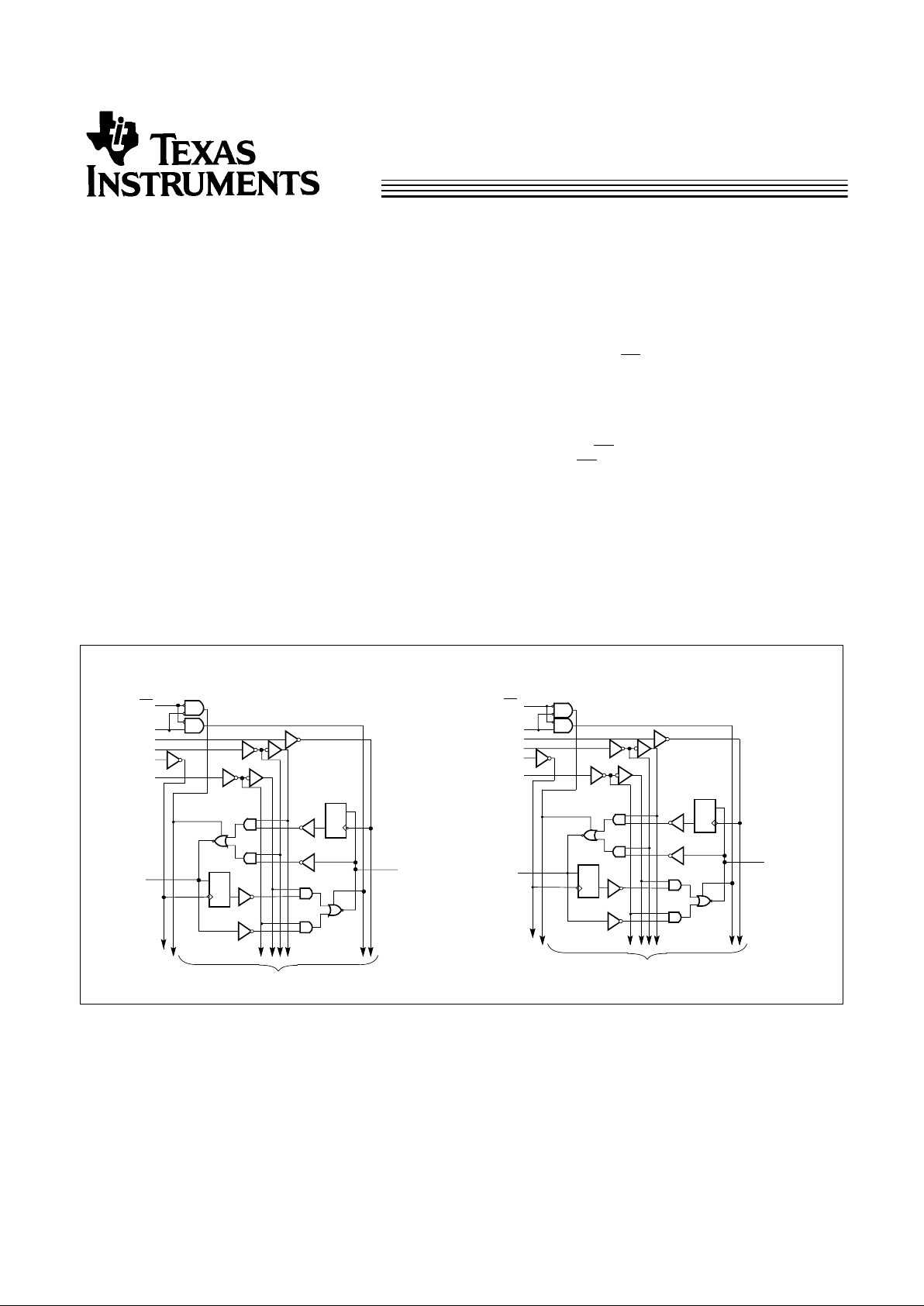
The CY74FCT163646 16-bit transceiver is a three-state,
D-type register, and control circuitry arranged for multiplexed
transmission of data directly from the input bus or from the
internal registers. Data on the A or B bus will be clocked into
the registers as the appropriate clock pin goes to a HIGHlogic
level. Output Enable (
OE) and direction pins (DIR) are
provided to control the transceiver function. In the transceiver
mode, data present at the high impedance port may be stored
in either the A or B register,or in both. The select controls can
multiplex stored and real-time (transparent mode) data. The
direction control determines which bus will receive data when
the Output Enable (
OE) is Active LOW. In the isolation mode
(Output Enable (
OE) HIGH), A data may be stored in the B
register and/or B data may be stored in the A register.
The CY74FCT163646 has 24-mA balanced output drivers
with current limiting resistors in the outputs. This reduces the
need for external terminating resistors and provides for
minimal undershoot and reduced ground bounce. The inputs
and outputs were designed to be capable of being driven by
5.0V buses, allowing them to be used in mixed voltage
systems as translators. The outputs are also designed with a
power-off disable feature enabling them to be used in
applications requiring live insertion.
Logic Block Diagrams
C
D
1
B
1
C
D
1
A
1
TO7 OTHER CHANNELS
1
SAB
1
CLKAB
1
CLKBA
1
DIR
1
SBA
1
OE
B REG
A REG
C
D
2
B
1
C
D
2A1
2
SAB
2
CLKAB
2
CLKBA
2
DIR
2
SBA
2
OE
B REG
TO 7 OTHER CHANNELS
A REG
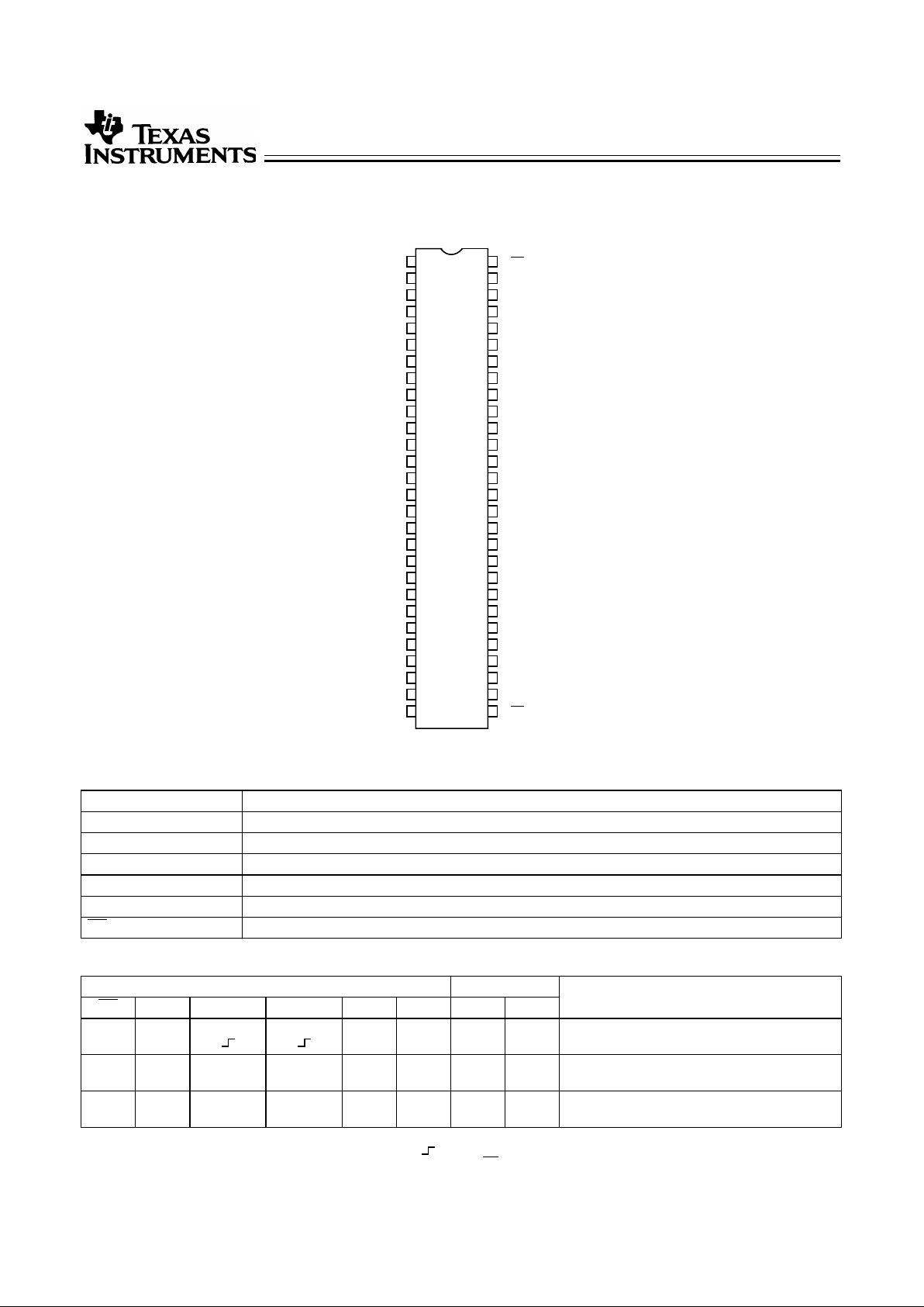
CY74FCT163646
2
GND
1
DIR
SSOP/TSSOP
Top View
1
CLKAB
1
SAB
1A1
1A2
1
CLKBA
1
SBA
1B1
1
OE
GND
GND
V
CC
1A3
V
CC
GND
1A4
1A5
1A6
1A7
1A8
2A1
2A2
2A3
2A4
GND
2A5
2A6
V
CC
2A7
2A8
2
SAB
2
CLKAB
1
2
3
4
5
6
7
8
9
10
11
12
13
14
15
16
17
18
19
20
21
22
23
24
25
26
27
28
56
55
54
53
52
51
50
49
48
47
46
45
44
43
42
41
40
39
38
37
36
35
34
33
32
31
30
29
GND
2
DIR
1B2
1B3
1B4
1B5
1B6
1B7
1B8
2B1
2B2
2B3
GND
2B4
2B5
2B6
V
CC
2B7
2B8
GND
2
SBA
2
CLKBA
2
OE
Pin Configuration
Pin Description
Pin Names Description
A Data Register A Inputs Data Register B Outputs
B Data Register B Inputs Data Register A Outputs
CLKAB, CLKBA Clock Pulse Inputs
SAB, SBA Output Data Source Select Inputs
DIR Direction
OE Output Enable (Active LOW)
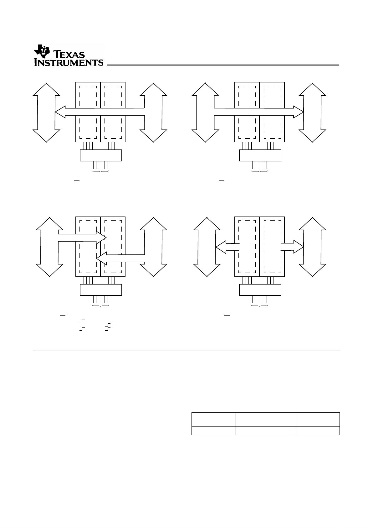
Function Table
[1]
Inputs Data I/O
[2]
Function
OE DIR CLKAB CLKBA SAB SBA A B
H
H
X
X
H or L H or L X
X
X
X
Input Input Isolation
Store A and B Data
L
L
L
L
X
X
X
H or L
X
X
LHOutput Input Real Time B Data to A Bus
Stored B Data to A Bus
L
L
H
H
X
H or L
X
X
L
H
X
X
Input Output Real Time A Data to Bus
Stored A Data to B Bus
Notes:
1. H = HIGH Voltage Level, L = LOW Voltage Level, X = Don’t Care, = LOW-to-HIGH Transition
2. The data output functions may be enabled or disabled by various signals at the
OE or DIR inputs. Data input functions are always enabled, i.e., data at the
bus pins will be stored on every LOW-to-HIGH transition on the clock inputs.
CY74FCT163646
3
Maximum Ratings
[4]
(Above which the useful life may be impaired. For user
guidelines, not tested.)
Storage Temperature ............................... −55°C to +125°C
Ambient Temperature with
Power Applied............................................ −55°C to +125°C
Supply Voltage Range ..................................... 0.5V to +4.6V
DC Input Voltage .................................................−0.5V to +7.0V
DC Output Voltage..............................................−0.5V to +7.0V
DC Output Current
(Maximum Sink Current/Pin)...........................−60 to +120 mA
Power Dissipation..........................................................1.0W
Static Discharge Voltage............................................>2001V
(per MIL-STD-883, Method 3015)
Notes:
3. Cannot transfer data to A-bus and B-bus simultaneously.
4. Stresses greaterthan those listed under Maximum Ratingsmay cause permanent damage tothedevice. This is astress rating only and functionaloperation of
the deviceat these or any other conditionsabove those indicated in the operationalsections of this specification is notimplied. Exposure to absolute maximum
rating conditions for extended periods may affect reliability.
BUS BBUS A
DIRLOELCLKAB
X
SAB
X
BUS BBUS A
DIR
H
L
X
OE
L
L
H
CLKAB
X
SAB
X
X
X
SBA
X
X
X
BUS
BBUS A
DIRHOE
L
SAB
L
SBA
X
BUS ABUS A
DIR
L
H
OE
L
L
SAB
X
H
SBA
H
X
Real-Time Transfer
BusB to BusA
Real-TimeTransfer
BusA to Bus B
Storagefrom
A and/or B
TransferStoredData
to A and/orB
CLKBA
X
CLKABXCLKBA
X
SBA
L
CLKBA
X
CLKAB
X
HorL
CLKBA
HorL
X
[3]
Operating Range
Range
Ambient
Temperature V
CC
Industrial –40°C to +85°C 2.7V to 3.6V

CY74FCT163646
4
Electrical Characteristics Over the Operating Range V
CC
=2.7V to 3.6V
Parameter Description Test Conditions Min. Typ.
[5]
Max. Unit
V
IH
Input HIGH Voltage All Inputs 2.0 5.5 V
V
IL
Input LOW Voltage 0.8 V
V
H
Input Hysteresis
[6]
100 mV
V
IK
Input Clamp Diode Voltage VCC=Min., IIN=−18 mA −0.7 −1.2 V
I
IH
Input HIGH Current VCC=Max., VI=5.5V ±1 µA
I
IL
Input LOW Current VCC=Max., VI=GND ±1 µA
I
OZH
High Impedance Output Current
(Three-State Output pins)
VCC=Max., V
OUT
=5.5V ±1 µA
I
OZL
High Impedance Output Current
(Three-State Output pins)
VCC=Max., V
OUT
=GND ±1 µA
I
ODL
Output LOW Dynamic Current
[7]
VCC=3.3V, VIN=V
IH
or VIL, V
OUT
=1.5V
45 180 mA
I
ODH
Output HIGH Dynamic Current
[7]
VCC=3.3V, VIN=V
IH
or VIL, V
OUT
=1.5V
–45 –180 mA
V
OH
Output HIGH Voltage VCC=Min., IOH= –0.1 mA VCC–0.2 V
VCC=3.0V, IOH= –8 mA 2.4
[8]
3.0
VCC=3.0V, IOH= –24 mA 2.0 3.0
V
OL
Output LOW Voltage VCC=Min., IOL= 0.1mA 0.2 V
VCC=Min., IOL= 24 mA 0.3 0.5
I
OS
Short Circuit Current
[7]
VCC=Max., V
OUT
=GND –60 –135 –240 mA
I
OFF
Power-Off Disable VCC=0V, V
OUT
≤4.5V ±100 µA
Capacitance
[5]
(TA = +25˚C, f = 1.0 MHz)
Symbol Description
[9]
Conditions Typ. Max. Unit
C
IN
Input Capacitance VIN = 0V 4.5 6.0 pF
C
OUT
Output Capacitance V
OUT
=0V 5.5 8.0 pF
Notes:
5. Typical values are at V
CC
=3.3V, TA=+25˚C ambient.
6. This parameter is specified but not tested.
7. Not morethan one output shouldbe shorted at a time.Duration of short should notexceed one second. Theuse of high-speed testapparatus and/or sample
and hold techniques are preferable in order to minimize internal chip heating and more accurately reflect operational values. Otherwise prolonged shorting
ofa highoutput mayraise thechip temperaturewell abovenormal andthereby causeinvalidreadings inother parametricstests.Inany sequenceof parameter
tests, IOS tests should be performed last.
8. VOH=VCC–0.6 V at rated current.
9. This parameter is measured at characterization but not tested.

CY74FCT163646
5
Power Supply Characteristics
Parameter Description Test Conditions Typ.
[5]
Max. Unit
I
CC
Quiescent PowerSupply Current VCC=Max. VIN<0.2V
V
IN>VCC
−0.2V
0.1 10 µA
∆I
CC
Quiescent Power Supply Current
TTL Inputs HIGH
VCC=Max. VIN=VCC–0.6V
[10]
2.0 30 µA
I
CCD
Dynamic Power Supply
Current
[11]
VCC=Max., Outputs Open
DIR=OE=GND
One-Bit Toggling
50% Duty Cycle
VIN=VCCor
V
IN
=GND
50 75 µA/MHz
I
C
Total Power Supply Current
[12]
VCC=Max.,Outputs Open
f
o
=10 MHz (CLKBA)
50% Duty Cycle
DIR=
OE=GND
One-BitToggling, f
1
=5MHz,
50% Duty Cycle
VIN=VCCor
V
IN
=GND
0.5 0.8 mA
VIN=VCC–0.6V or
V
IN
=GND
0.5 0.8
VCC=Max., Outputs Open
f
o
=10 MHz (CLKBA)
50% Duty Cycle
DIR=
OE=GND
Sixteen-Bits Toggling
f
1
=2.5 MHz
50% Duty Cycle
VIN=VCCor
V
IN
=GND
2.5 3.8
[13]
VIN=VCC–0.6V or
V
IN
=GND
2.6 4.1
[13]
Notes:
10. Per TTL driven input); all other inputs at V
CC
or GND.
11. This parameter is not directly testable, but is derived for use in Total Power Supply calculations.
12. I
C
=I
QUIESCENT
+ I
INPUTS
+ I
DYNAMIC
IC=ICC+∆ICCDHNT+I
CCD(f0NC
/2 + f1N1)
I
CC
= Quiescent Current with CMOS input levels
∆I
CC
= Power Supply Current for a TTL HIGH input
D
H
= Duty Cycle for TTL inputs HIGH
N
T
= Number of TTL inputs at D
H
I
CCD
= Dynamic Current caused by an input transition pair (HLH or LHL)
f
0
= Clock frequency for registered devices, otherwise zero
N
C
= Number of clock inputs changing at f
1
f1= Input signal frequency
N
1
= Number of inputs changing at f
1
All currents are in milliamps and all frequencies are in megahertz.
13. Values for these conditions are examples of the I
CC
formula. These limits are specified but not tested.

CY74FCT163646
6
Switching Characteristics Over the Operating Range V
CC
=3.0V to 3.6V
[14,15]
Parameter Description
CY74FCT163646C
UnitMin. Max. Fig. No.
[16]
t
PLH
t
PHL
Propagation Delay Bus to Bus 1.5 5.4 ns 1, 2
t
PZH
t
PZL
Output Enable Time DIR or OE to Bus 1.5 7.8 ns 1, 7, 8
t
PHZ
t
PLZ
Output Disable Time DIR or OE to Bus 1.5 6.3 ns 1, 7, 8
t
PLH
t
PHL
Propagation Delay Clock to Bus 1.5 5.7 ns 1, 5
t
PLH
t
PHL
Propagation Delay SBA or SAB to Bus 1.5 6.2 ns 1,5
t
SU
Set-Up Time HIGH or LOW Bus to Clock 2.0 — ns 4
t
H
Hold Time HIGH or LOW Bus to Clock 1.5 — ns 4
t
W
Clock Pulse Width HIGH or LOW 5.0 — ns 6
t
SK(O)
Output Skew
[17]
— 0.5 ns —
Ordering Information CY74FCT163646
Speed
(ns) Ordering Code
Package
Name Package Type
Operating
Range
5.4 CY74FCT163646CPACT Z56 56-Lead (240-Mil) TSSOP Industrial
CY74FCT163646CPVC/PVCT O56 56-Lead (300-Mil) SSOP
Notes:
14. Minimum limits are specified but not tested on Propagation Delays.
15. For V
CC
=2.7, propagation delay, output enable and output disable times should be degraded by 20%.
16. See “Parameter Measurement Information” in the General Information section.
17. Skew any two outputs of the same package switching in the same direction. This parameter is ensured by design.

CY74FCT163646
7
Package Diagrams
56-Lead Shrunk Small Outline Package O56
56-Lead Thin Shrunk Small Outline Package Z56

IMPORTANT NOTICE
T exas Instruments and its subsidiaries (TI) reserve the right to make changes to their products or to discontinue
any product or service without notice, and advise customers to obtain the latest version of relevant information
to verify, before placing orders, that information being relied on is current and complete. All products are sold
subject to the terms and conditions of sale supplied at the time of order acknowledgement, including those
pertaining to warranty, patent infringement, and limitation of liability.
TI warrants performance of its semiconductor products to the specifications applicable at the time of sale in
accordance with TI’s standard warranty. Testing and other quality control techniques are utilized to the extent
TI deems necessary to support this warranty. Specific testing of all parameters of each device is not necessarily
performed, except those mandated by government requirements.
CERT AIN APPLICATIONS USING SEMICONDUCTOR PRODUCTS MAY INVOLVE POTENTIAL RISKS OF
DEATH, PERSONAL INJURY, OR SEVERE PROPERTY OR ENVIRONMENTAL DAMAGE (“CRITICAL
APPLICATIONS”). TI SEMICONDUCTOR PRODUCTS ARE NOT DESIGNED, AUTHORIZED, OR
WARRANTED TO BE SUITABLE FOR USE IN LIFE-SUPPORT DEVICES OR SYSTEMS OR OTHER
CRITICAL APPLICATIONS. INCLUSION OF TI PRODUCTS IN SUCH APPLICA TIONS IS UNDERSTOOD T O
BE FULLY AT THE CUSTOMER’S RISK.
In order to minimize risks associated with the customer’s applications, adequate design and operating
safeguards must be provided by the customer to minimize inherent or procedural hazards.
TI assumes no liability for applications assistance or customer product design. TI does not warrant or represent
that any license, either express or implied, is granted under any patent right, copyright, mask work right, or other
intellectual property right of TI covering or relating to any combination, machine, or process in which such
semiconductor products or services might be or are used. TI’s publication of information regarding any third
party’s products or services does not constitute TI’s approval, warranty or endorsement thereof.
Copyright 2000, Texas Instruments Incorporated
 Loading...