Texas Instruments CY74FCT163H501CPVC, CY74FCT163H501CPAC, CY74FCT163501CPVCT, CY74FCT163501CPVC, CY74FCT163501CPACT Datasheet
...
18-Bit Registered Transceivers
CY74FCT163501
CY74FCT163H501
SCCS047 - January 1998 - Revised March 2000
Data sheet acquired from Cypress Semiconductor Corporation.
Data sheet modified to remove devices not offered.
Copyright © 2000, Texas Instruments Incorporated
Features
• Low power, pin-compatible replacement for LCX and
LPT families
• 5V tolerant inputs and outputs
• 24 mA balanced drive outputs
• Power-off disable outputs permits live insertion
• Edge-rate control circuitry for reduced noise
• FCT-C speed at 4.6 ns
• Latch-up performance exceedsJEDEC standard no. 17
• ESD > 2000V per MIL-STD-883D, Method 3015
• Typical output skew < 250ps
• Industrial temperature range of –40˚C to +85˚C
• TSSOP (19.6-mil pitch) or SSOP (25-mil pitch)
• TypicalV
olp
(groundbounce)performanceexceedsMil
Std 883D
•V
CC
= 2.7V to 3.6V
CY74FCT163501 Features:
• Balanced output drivers: 24 mA
• Reduced system switching noise
• Typical V
OLP
(ground bounce) <0.6V at VCC = 3.3V,
TA= 25˚C
CY74FCT163H501 Features:
• Bus hold retains the last active state
• Devices with bus hold are not recommended for translating rail-to-rail CMOS signals to 3.3V logic levels
• Eliminates the need for external pull-up or pull-down
resistors
Functional Description
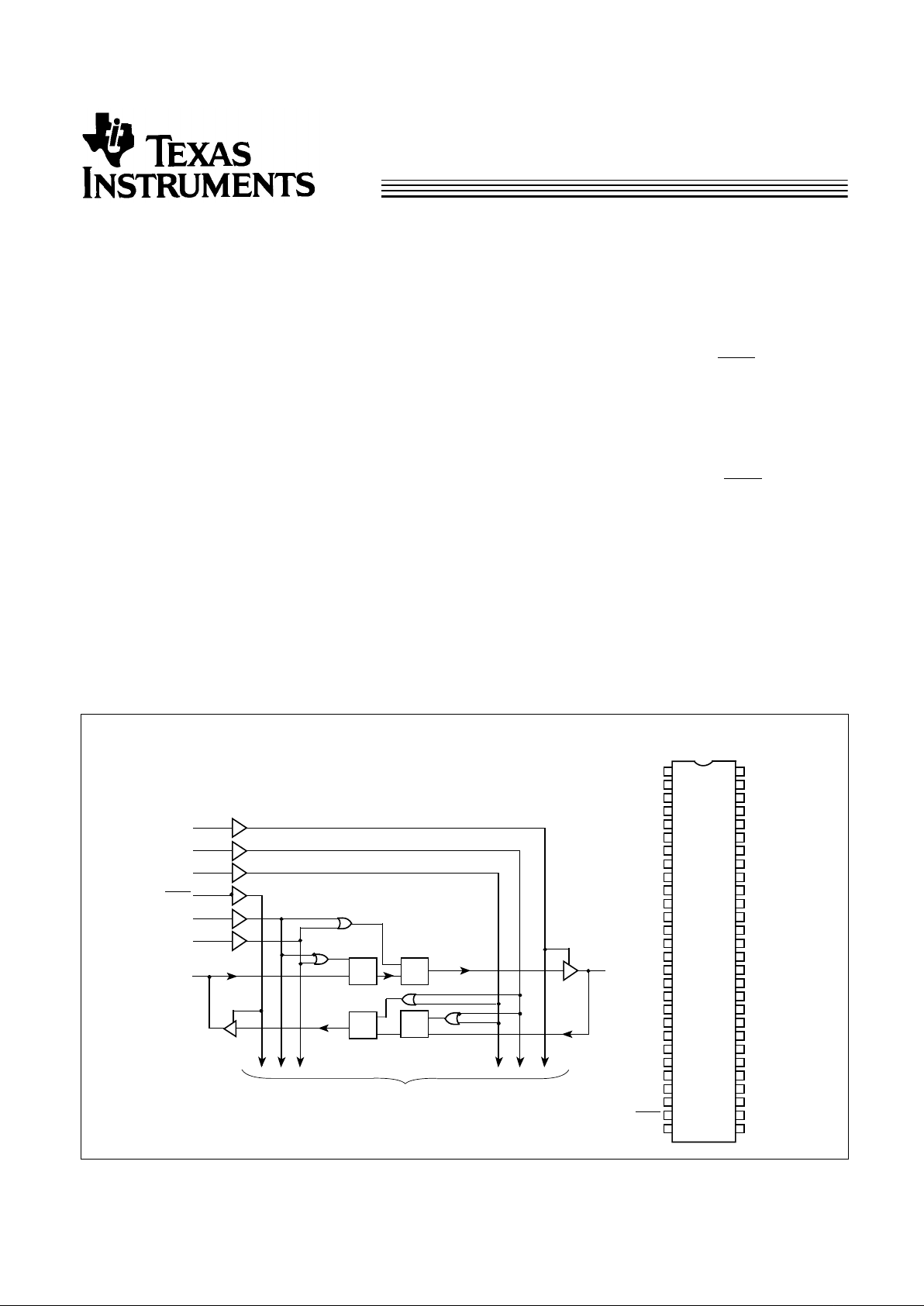
These 18-bit universal bus transceivers can be operated in
transparent, latched or clock modes by combining D-type
latches and D-type flip-flops. Data flow in each direction is
controlled by output enable (OEAB and
OEBA), latch enable
(LEAB and LEBA), and clock inputs (CLKAB andCLKBA). For
A-to-B data flow, the device operates in transparent mode
when LEAB is HIGH. When LEAB is LOW, the A data is
latched if CLKAB is held at a HIGHor LOWlogiclevel.IfLEAB
is LOW, the A bus data is stored in the latch/flip-flop on the
LOW-to-HIGHtransition of CLKAB.OEABperformstheoutput
enable function on the B port. Data flow from B-to-A is similar
to that of A-to-B and is controlled by
OEBA, LEBA, and
CLKBA. The output buffers are designed with a power-off
disable feature to allow live insertion of boards.
THE CY74FCT163501 has 24-mA balanced output drivers
with current limiting resistors in the outputs. This reduces the
need for external terminating resistors, as well as provides for
minimal undershoot and reduced ground bounce. The
CY74FCT163501 is ideal for driving transmission lines.
The CY74FCT163H501 is a 24-mA balanced output part, that
has “bus hold” on the data inputs. The device retains the
input’s last state whenever the input goes to high impedance.
This eliminates the need for pull-up/down resistors and
prevents floating inputs.
GND
Functional Block Diagram; CY74FCT163501, CY74FCT163H501
Pin
Configuration
1
2
3
4
5
6
7
8
9
10
11
12
OEAB
SSOP/TSSOP
Top View
13
14
15
16
17
18
19
20
21
22
23
24
LEAB
A
1
GND
GND
V
CC
GND
GND
FCT163501-1
A
2
A
3
A
4
A
5
A
6
A
7
A
8
A
9
GND
25
26
27
28
GND
A
10
A
11
A
12
V
CC
A
13
A
14
A
15
A
16
A
17
A
18
OEBA
LEBA
56
55
54
53
52
51
50
49
48
47
46
45
44
43
42
41
40
39
38
37
36
35
34
33
32
31
30
29
GND
CLKAB
B
1
GND
B
2
B
3
V
CC
B
4
B
5
B
6
GND
B
7
B
8
B
9
B
10
B
11
B
12
B
13
B
14
B
15
V
CC
B
16
B
17
B
18
CLKBA
OEAB
CLKBA
LEBA
OEBA
CLKAB
LEAB
C
D
C
D
C
D
A
1
B
1
C
D
TO 17 OTHER CHANNELS
FCT163501-2

CY74FCT163501
CY74FCT163H501
2
Maximum Ratings
[6, 7]
(Above which the useful life may be impaired. For user
guidelines, not tested.)
Storage Temperature .....................................−55°C to +125°C
Ambient Temperature with
Power Applied..................................................−55°C to +125°C
DC Input Voltage .................................................−0.5V to +7.0V
DC Output Voltage..............................................−0.5V to +7.0V
DC Output Current
(Maximum Sink Current/Pin)...........................−60 to +120 mA
Power Dissipation..........................................................1.0W
Static Discharge Voltage............................................>2001V
(per MIL-STD-883, Method 3015)
1. On the 74FCT163H501 these pins have bus hold.
2. A-to-B data flow is shown. B-to-A data flow is similar but uses OEBA, LEBA, and CLKBA.
3. H = HIGH Voltage Level
L = LOW Voltage Level
X = Don’t Care
Z = High-impedance
= LOW-to-HIGH Transition
4. Output level before the indicated steady-state input conditions were established.
5. Output level before the indicated steady-state input conditions were established, provided that CLKAB was HIGH before LEAB went LOW.
6. Operationbeyondthe limits setforth may impair theusefullife of thedevice.Unlessotherwise noted,theselimits are overtheoperating free-air temperaturerange.
7. Unused inputs must always be connected to an appropriate logic voltage level, preferably either VCC or ground.
Pin Description
Name Description
OEAB A-to-B Output Enable Input
OEBA B-to-A Output Enable Input (Active LOW)
LEAB A-to-B Latch Enable Input
LEBA B-to-A Latch Enable Input
CLKAB A-to-B Clock Input
CLKBA B-to-A Clock Input
A A-to-B Data Inputs or B-to-A Three-State
Outputs
[1]
B B-to-A Data Inputs or A-to-B Three-State
Outputs
[1]
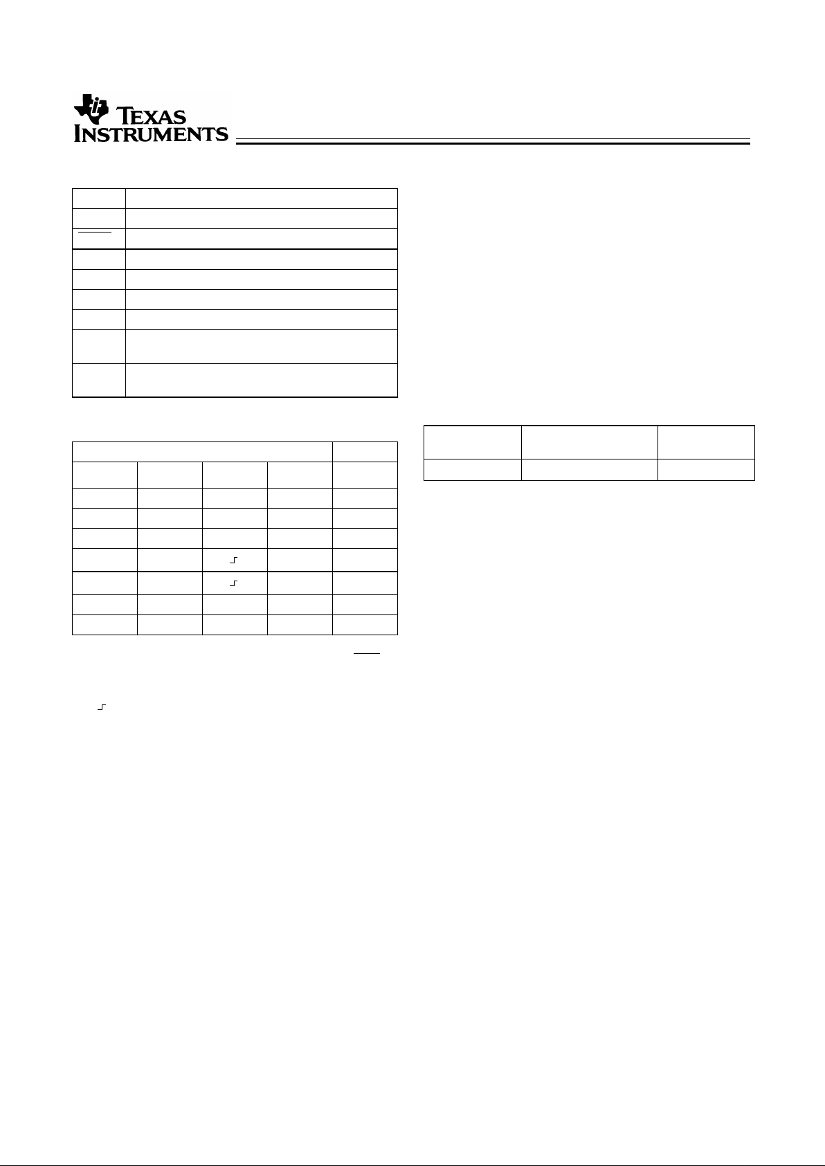
Function Table
[2, 3]
Inputs Outputs
OEAB LEAB CLKAB A B
L X X X Z
H H X L L
H H X H H
H L L L
H L H H
H L L X B
[4]
H L H X B
[5]
Operating Range
Range
Ambient
Temperature V
CC
Industrial −40°C to +85°C 2.7V to 3.6V

CY74FCT163501
CY74FCT163H501
3
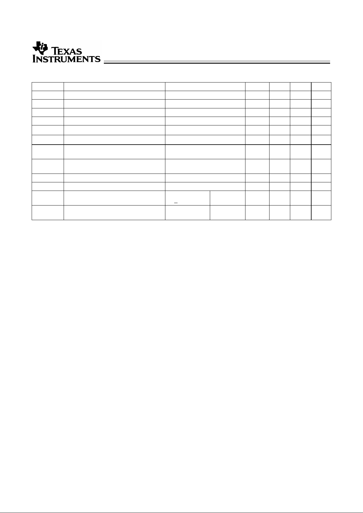
Electrical Characteristics for Non Bus Hold Devices Over the Operating Range V
CC
= 2.7V to 3.6V
Parameter Description Test Conditions Min. Typ.
[8]
Max. Unit
V
IH
Input HIGH Voltage All Inputs 2.0 5.5 V
V
IL
Input LOW Voltage 0.8 V
V
H
Input Hysteresis
[9]
100 mV
V
IK
Input Clamp Diode Voltage VCC=Min., IIN=–18 mA –0.7 –1.2 V
I
IH
Input HIGH Current VCC=Max., VI=5.5 ±1 µA
I
IL
Input LOW Current VCC=Max., VI=GND ±1 µA
I
OZH
High Impedance Output Current
(Three-State Output pins)
VCC=Max., V
OUT
=5.5V ±1 µA
I
OZL
High Impedance Output Current
(Three-State Output pins)
VCC=Max., V
OUT
=GND ±1 µA
I
OS
Short Circuit Current
[10]
VCC=Max., V
OUT
=GND –60 –135 –240 mA
I
OFF
Power-Off Disable VCC=0V, V
OUT
≤4.5V ±100 µA
I
CC
Quiescent Power Supply Current VIN≤0.2V,
V
IN>VCC
–0.2V
VCC=Max. 0.1 10 µA
∆I
CC
Quiescent Power Supply Current
(TTL inputs HIGH)
VIN=VCC–0.6V
[11]
VCC=Max. 2.0 30 µA
Notes:
8. Typical values are at V
CC
=3.3V, TA = +25˚C ambient.
9. This parameter is specified but not tested.
10. Not more than one output should be shorted at a time. Duration of short should not exceed one second. The use of high-speed test apparatus and/or sample
and hold techniques are preferablein order to minimize internal chip heating and more accurately reflect operational values. Otherwise prolonged shorting of
a high output may raise the chip temperature well above normal and thereby cause invalid readings in other parametric tests. In any sequence of parameter
tests, I
OS
tests should be performed last.
11. Per TTL driven input (V
IN
=3.4V); all other inputs at VCC or GND.
 Loading...