

TEXAS INSTRUMENTS CY74FCT163244 Technical data
查询74FCT163H244CPACT供应商
Data sheet acquired from Cypress Semiconductor Corporation.
Data sheet modified to remove devices not offered.
CY74FCT163244
CY74FCT163H244
SCCS046 - December 1996 - Revised March 2000
Features
• Low power, pin-compatible replacement for LCX and
LPT families
• 5V tolerant inputs and outputs
• 24 mA balanced drive outputs
CY74FCT163H244
• Bus hold on data inputs
• Eliminates the need for external pull-up or pull-down
resistors
• Devices with bus hold are not recommended for translating rail-to-rail CMOS signals to 3.3V logic levels
• Power-off disable outputs permits live insertion
• Edge-rate control circuitry for reduced noise
• FCT-C speed at 4.1 ns
• Latch-up performance exceedsJEDEC standard no. 17
• Typical output skew < 250 ps
• Industrial temperature range of –40˚C to +85˚C
• TSSOP (19.6-mil pitch) or SSOP (25-mil pitch)
• Typical
Std 883D
•V
V
olp
= 2.7V to 3.6V
CC
(groundbounce)performanceexceedsMil
• ESD (HBM) > 2000V
Functional Description
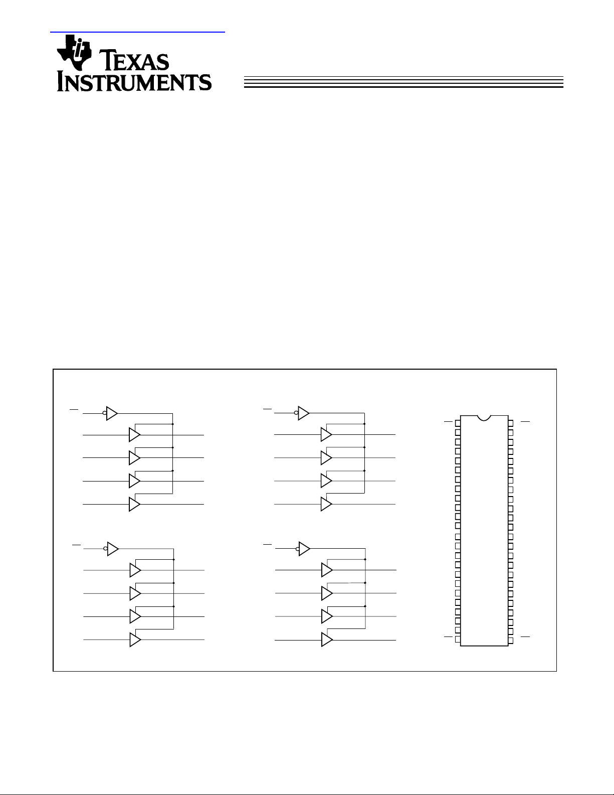
These 16-bit buffers/line drivers are designed for use in
memory driver,clockdriver,or other businterface applications,
wherehigh-speed and low powerare required. Thethree-state
controls are designed to allow 4-bit, 8-bit or combined 16-bit
operation. Flow-through pinout and small shrink packaging
simplifies board layout.
The CY74FCT163244 has 24-mA balanced output drivers
with current limiting resistors in the outputs.
The CY74FCT163H244 has “bus hold” on the data inputs,
which retains the last state of the input whenever the source
driving the input goes to high impedance. This eliminates the
need for pull-up/down resistors and prevents floating inputs.
Logic Block Diagrams CY74FCT163244, CY74FCT163H244
OE
1
1A1
1A2
1A3
1A4
2
OE
2A1
2A2
2A3
2A4
1Y1
1Y2
1Y3
1Y4
2Y1
2Y2
2Y3
2Y4
OE
3
3A1
3A2
3A3
3A4
OE
4
4A1
4A2
4A3
4A4
16-Bit Buffers/Line Drivers
Pin
Configuration
SSOP/TSSOP
Top View
3Y1
3Y2
3Y3
3Y4
4Y1
4Y2
4Y3
4Y4
OE
1
1Y1
1Y2
GND
1Y3
1Y4
V
2Y1
2Y2
GND
2Y3
2Y4
3Y1
3Y2
GND
3Y3
3Y4
V
4Y1
4Y2
GND
4Y3
4Y4
OE
4
1
2
3
4
5
6
CC
7
8
9
10
11
12
13
14
15
16
17
18
CC
19
20
21
22
23
24
163244
163H244
48
OE
2
47
1A1
46
1A2
GND
45
44
1A3
43
1A4
V
CC
42
2A1
41
2A2
40
GND
39
2A3
38
37
2A4
36
3A1
35
3A2
34
GND
33
3A3
32
3A4
31
V
CC
30
4A1
29
4A2
GND
28
27
4A3
26
4A4
OE
3
25
Copyright © 2000, Texas Instruments Incorporated
CY74FCT163244
CY74FCT163H244
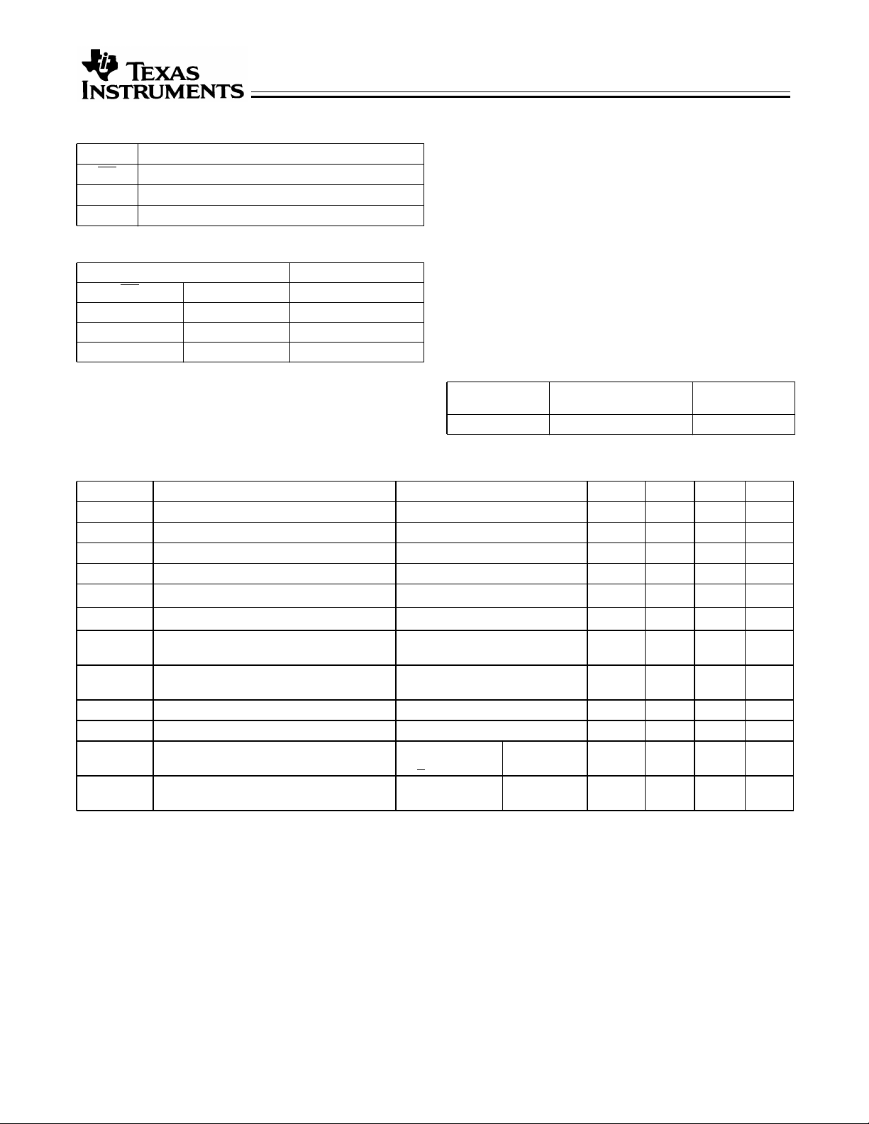
Pin Description
Name Description
OE Three-State Output Enable Inputs (Active LOW)
A Data Inputs
Y Three-State Outputs
Function Table
Inputs Outputs
OE A Y
L L L
L H H
[1]
[2]
Maximum Ratings
(Above which the useful life may be impaired. For user guidelines, not tested.)
Storage Temperature................................. –55°C to +125°C
Ambient Temperature with
Power Applied............................................ –55°C to +125°C
Supply Voltage Range..................................... 0.5V to +4.6V
DC Input Voltage ........................................... –0.5V to +7.0V
DC Output Voltage......................................... –0.5V to +7.0V
DC Output Current
(Maximum Sink Current/Pin) ........................–60 to +120 mA
Power Dissipation..........................................................1.0W
[3,4]
H X Z
Operating Range
Range
Industrial –40°C to +85°C 2.7V to 3.6V
Electrical Characteristics for Non Bus Hold Devices Over the Operating Range V
Parameter Description Test Conditions Min. Typ.
V
IH
V
IL
V
H
V
IK
I
IH
I
IL
I
OZH
I
OZL
I
OS
I
OFF
I
CC
∆I
CC
Notes:
1. On the CY74FCT163H244, these pins have “bus hold.”
2. H = HIGH Voltage Level. L = LOW Voltage Level. X = Don’t Care. Z = High Impedance.
3. Operation beyond the limits set forth may impair the useful life of the device. Unless otherwise noted, these limits are over the operating free-air temperature
range.
4. With the exception of inputs with bus hold, unused inputs must always be connected to an appropriate logic voltage level, preferably either V
5. Typical values are at V
6. This parameter is specified but not tested.
7. Not more than one output should be shorted at a time. Duration of short should not exceed one second. The use of high-speed test apparatus and/or sample
and hold techniques are preferable in order to minimize internalchip heating and more accurately reflect operational values. Otherwise prolonged shorting of
a high output may raise the chip temperature well above normal and thereby cause invalid readings in other parametric tests. In any sequence of parameter
tests, I
8. Per TTL driven input; all other inputs at V
Input HIGH Voltage All Inputs 2.0 5.5 V
Input LOW Voltage 0.8 V
Input Hysteresis
[6]
Input Clamp Diode Voltage VCC=Min., IIN=–18 mA –0.7 – 1.2 V
Input HIGH Current VCC=Max., VI=5.5 ±1 µA
Input LOW Current VCC=Max., VI=GND ±1 µA
High Impedance Output Current
(Three-State Output pins)
High Impedance Output Current
(Three-State Output pins)
Short Circuit Current
[7]
Power-Off Disable VCC=0V, V
Quiescent Power Supply Current VIN≤0.2V,
Quiescent Power Supply Current
VCC=Max., V
VCC=Max., V
VCC=Max., V
OUT
V
IN>VCC
–0.2V
VIN=VCC–0.6V
=5.5V ±1 µA
OUT
=GND ±1 µA
OUT
=GND –60 –135 –240 mA
OUT
≤4.5V ±100 µA
VCC=Max. 0.1 10 µA
[8]
VCC=Max. 2.0 30 µA
(TTL inputs HIGH)
=3.3V, TA = +25˚C ambient.
CC
tests should be performed last.
OS
or GND.
CC
Ambient
Temperature V
=2.7V to 3.6V
CC
[5]
Max. Unit
100 mV
or ground.
CC
CC
2

CY74FCT163244
CY74FCT163H244
Electrical Characteristics For Bus Hold Devices Over the Operating Range V
=2.7V to 3.6V
CC
Parameter Description Test Conditions Min. Typ.
V
IH
V
IL
V
H
V
IK
I
IH
I
IL
I
BBH
I
BBL
I
BHHO
I
BHLO
I
OZH
I
OZL
I
OS
I
OFF
I
CC
∆
ICC
Input HIGH Voltage All Inputs 2.0 V
Input LOW Voltage 0.8 V
Input Hysteresis
[6]
Input Clamp Diode Voltage VCC=Min., IIN=–18 mA –0.7 –1.2 V
Input HIGH Current VCC=Max., VI=V
CC
Input LOW Current ±100 µA
Bus Hold Sustain Current on Bus Hold Input
[9]
VCC=Min. VI=2.0V –50 µA
VI=0.8V +50 µA
Bus Hold Overdrive Current on Bus Hold In-
[9]
put
High Impedance Output Current
(Three-State Output pins)
High Impedance Output Current
(Three-State Output pins)
Short Circuit Current
[7]
Power-Off Disable VCC=0V, V
Quiescent Power Supply Current VIN≤0.2V,
Quiescent Power supply Current
(TTL inputs HIGH)
VCC=Max., VI=1.5V ±500 µA
VCC=Max., V
VCC=Max., V
VCC=Max., V
V
IN>VCC
VIN=VCC–0.6V
OUT=VCC
=GND ±1 µA
OUT
=GND –60 –135 –240 mA
OUT
≤4.5V ±100 µA
OUT
VCC=Max.
–0.2V
[8]
VCC=Max.
[5]
Max. Unit
CC
V
100 mV
±100 µA
±1 µA
+40 µA
+350 µA
Electrical Characteristics For Balanced Drive Devices Over the Operating Range V
CC
Parameter Description Test Conditions Min. Typ.
I
ODL
I
ODH
V
OH
Output LOW Dynamic Current
Output HIGH Dynamic Current
Output HIGH Voltage VCC=Min., IOH= –0.1 mA VCC–0.2 V
[7]
[7]
VCC=3.3V, VIN=V
or VIL, V
OUT
VCC=3.3V, VIN=V
or VIL, V
OUT
=1.5V
=1.5V
IH
IH
–45 –180 mA
VCC=3.0V, IOH= –8 mA 2.4
45 180 mA
[10]
VCC=3.0V, IOH= –24 mA 2.0 3.0 V
V
OL
Output LOW Voltage VCC=Min., IOL= 0.1mA 0.2 V
VCC=Min., IOL= 24 mA 0.3 0.55
Notes:
9. Pins with bus hold are described in Pin Description.
10. V
= VCC – 0.6V at rated current.
OH
=2.7V to 3.6V
[5]
Max. Unit
3.0 V
3
 Loading...