Texas Instruments CY74FCT16823CTPVC, CY74FCT16823CTPACT, CY74FCT16823CTPAC, CY74FCT16823ATPACT, CY74FCT16823ATPAC Datasheet
...
18-Bit Registers
CY74FCT16823T
CY74FCT162823T
SCCS062 - August 1994 - Revised March 2000
Data sheet acquired from Cypress Semiconductor Corporation.
Data sheet modified to remove devices not offered.
Copyright © 2000, Texas Instruments Incorporated
Features
• FCT-E speed at 4.4 ns
• Power-off disable outputs permits live insertion
• Edge-rate control circuitry for significantly improved
noise characteristics
• Typical output skew < 250 ps
• ESD > 2000V
• TSSOP (19.6-mil pitch) and SSOP (25-mil pitch)
packages
• Industrial temperature range of −40˚C to +85˚C
•V
CC
= 5V ± 10%
CY74FCT16823T Features:
• 64 mA sink current, 32 mA source current
• Typical V
OLP
(ground bounce) <1.0V at VCC = 5V,
TA = 25˚C
CY74FCT162823T Features:
• Balanced 24 mA output drivers
• Reduced system switching noise
• Typical V
OLP
(ground bounce) <0.6V at VCC = 5V,
TA= 25˚C
Functional Description
The CY74FCT16823T and the CY74FCT162823T 18-bit bus
interface registers are designed for use in high-speed,
low-power systems needing wide registers and parity. 18-bit
operationisachievedbyconnectingthecontrollinesofthetwo
9-bit registers. Flow-through pinout and small shrink
packaging aids in simplifying board layout. The outputs are
designedwitha power-offdisablefeaturetoallowliveinsertion
of boards.
The CY74FCT16823T is ideally suited for driving
high-capacitance loads and low-impedance backplanes.
The CY74FCT162823T has 24-mA balanced output drivers
with current limiting resistors in the outputs. This reduces the
need for external terminating resistors and provides for
minimal undershoot and reduced ground bounce. The
CY74FCT162823T is ideal for driving transmission lines.
Logic Block Diagrams
C
Pin Configuration
D
R
1
2
3
4
5
6
7
8
9
10
11
12
33
32
31
30
29
36
35
1
CLR
34
SSOP/TSSOP
Top View
13
15
16
17
18
19
20
21
22
23
24
45
44
43
42
41
37
38
39
40
48
47
46
1
CLR
1D1
1
OE
1
OE
1Q1
1Q2
GND
V
CC
GND
FCT16823-1
1
CLK
1
CLKEN
1Q1
TO 8 OTHER CHANNELS
GND
1D1
1D2
1D3
1D4
1
CLK
GND
1D5
1D6
1D7
1D9
V
CC
GND
2D1
2D2
2D4
GND
2D5
2D6
2D7
2D8
V
CC
2
CLK
1
CLKEN
25
26
27
28
49
50
51
52
53
54
55
56
1D8
2D3
2D9
2
CLKEN
C
D
R
2
CLR
2D2
2
OE
2
CLK
2
CLKEN
2Q1
TO 8 OTHER CHANNELS
1Q3
1Q4
1Q5
1Q7
1Q8
1Q9
1Q6
14
2Q1
2Q2
2Q3
2Q4
2Q6
2Q7
2Q8
2Q5
2Q9
GND
V
CC
GND
2
OE
2
CLR
FCT16823-2
FCT16823-3

CY74FCT16823T
CY74FCT162823T
2
Maximum Ratings
[3, 4]
(Above which the useful life may be impaired. For user
guidelines, not tested.)
Storage Temperature .....................................−55°C to +125°C
Ambient Temperature with
Power Applied..................................................−55°C to +125°C
DC Input Voltage .................................................−0.5V to +7.0V
DC Output Voltage..............................................−0.5V to +7.0V
DC Output Current
(Maximum Sink Current/Pin)...........................−60 to +120 mA
Power Dissipation..........................................................1.0W
Static Discharge Voltage............................................>2001V
(per MIL-STD-883, Method 3015)
Notes:
1. H = HIGH Voltage Level.
L = LOW Voltage Level.
X = Don’t Care.
Z = HIGH Impedance.
=LOW-to-HIGH transition.
2. Output level before indicated steady-state input conditions were established.
3. Operationbeyondthe limitssetforth mayimpairtheuseful lifeofthe device.Unless otherwisenoted, theselimits areover theoperating free-airtemperature range.
4. Unused inputs must always be connected to an appropriate logic voltage level, preferably either V
CC
or ground.
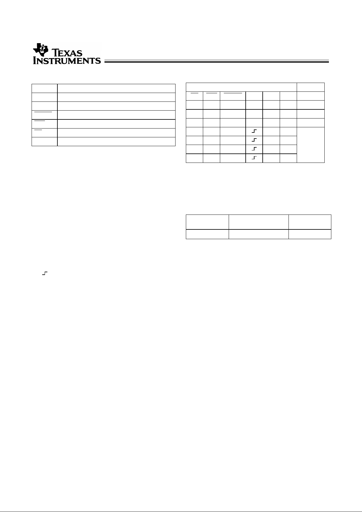
Pin Description
Name Description
D Data Inputs
CLK Clock Inputs
CLKEN Clock Enable Inputs (Active LOW)
CLR Asynchronous Clear Inputs (Active LOW)
OE Output Enable Inputs (Active LOW)
Q Three-State Outputs
Function Table
[1]
Inputs Outputs
OE CLR CLKEN CLK D Q Function
H X X X X Z High Z
L L X X X L Clear
L H H X X Q
[2]
Hold
H H L L Z Load
H H L H Z
L H L L L
L H L H H
Operating Range
Range
Ambient
Temperature V
CC
Industrial −40°C to +85°C 5V ± 10%

CY74FCT16823T
CY74FCT162823T
3
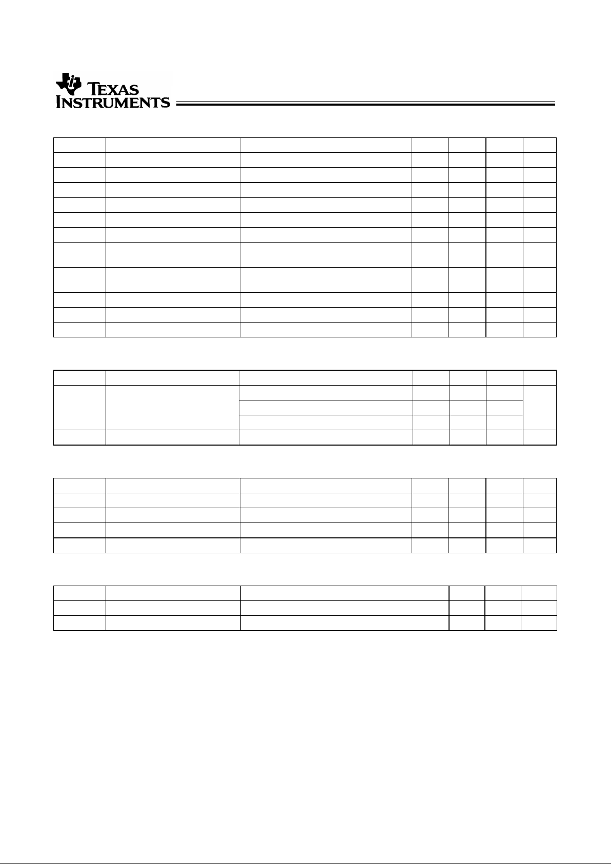
Electrical Characteristics Over the Operating Range
Parameter Description Test Conditions Min. Typ.
[5]
Max. Unit
V
IH
Input HIGH Voltage 2.0 V
V
IL
Input LOW Voltage 0.8 V
V
H
Input Hysteresis
[6]
100 mV
V
IK
Input Clamp Diode Voltage VCC=Min., IIN=−18 mA −0.7 −1.2 V
I
IH
Input HIGH Current VCC=Max., VI=V
CC
±1 µA
I
IL
Input LOW Current VCC=Max., VI=GND ±1 µA
I
OZH
HighImpedanceOutputCurrent
(Three-State Output pins)
VCC=Max., V
OUT
=2.7V ±1 µA
I
OZL
HighImpedanceOutputCurrent
(Three-State Output pins)
VCC=Max., V
OUT
=0.5V ±1 µA
I
OS
Short Circuit Current
[7]
VCC=Max., V
OUT
=GND −80 −140 −200 mA
I
O
Output Drive Current
[7]
VCC=Max., V
OUT
=2.5V −50 −180 mA
I
OFF
Power-Off Disable VCC=0V, V
OUT
≤4.5V
[8]
1 µA
Output Drive Characteristics for CY74FCT16823T
Parameter Description Test Conditions Min. Typ.
[5]
Max. Unit
V
OH
Output HIGH Voltage VCC=Min., IOH=−3 mA 2.5 3.5 V
VCC=Min., IOH=−15 mA 2.4 3.5
VCC=Min., IOH=−32 mA 2.0 3.0
V
OL
Output LOW Voltage VCC=Min., IOL=64 mA 0.2 0.55 V
Output Drive Characteristics for CY74FCT162823T
Parameter Description Test Conditions Min. Typ.
[5]
Max. Unit
I
ODL
Output LOW Voltage
[7]
VCC=5V, VIN=VIH or VIL, V
OUT
=1.5V 60 115 150 mA
I
ODH
Output HIGH Voltage
[7]
VCC=5V, VIN=VIH or VIL, V
OUT
=1.5V −60 −115 −150 mA
V
OH
Output HIGH Voltage VCC=Min., IOH=−24 mA 2.4 3.3 V
V
OL
Output LOW Voltage VCC=Min., IOL=24 mA 0.3 0.55 V
Capacitance
[9]
(TA = +25˚C, f = 1.0 MHz)
Parameter Description Test Conditions Typ.
[5]
Max. Unit
C
IN
Input Capacitance VIN = 0V 4.5 6.0 pF
C
OUT
Output Capacitance V
OUT
= 0V 5.5 8.0 pF
Notes:
5. Typical values are at V
CC
= 5.0V, TA= +25˚C ambient.
6. This input is specified but not tested.
7. Not more than one outputshouldbe shorted at a time.Duration of short should not exceed one second.Theuse of high-speed test apparatus and/or sample
and hold techniques are preferable in order to minimize internal chip heating and more accurately reflect operational values. Otherwise prolonged shorting
of ahigh output mayraise the chip temperaturewell above normalandthereby cause invalidreadings in otherparametric tests. In anysequence of parameter
tests, I
OS
tests should be performed last.
8. Tested at+25˚C.
9. This parameter is specified but not tested.
 Loading...