

Page 1
MSP50C30
MIXED-SIGNAL PROCESSOR
SPSS021 NOVEMBER 1998
1
POST OFFICE BOX 655303 • DALLAS, TEXAS 75265
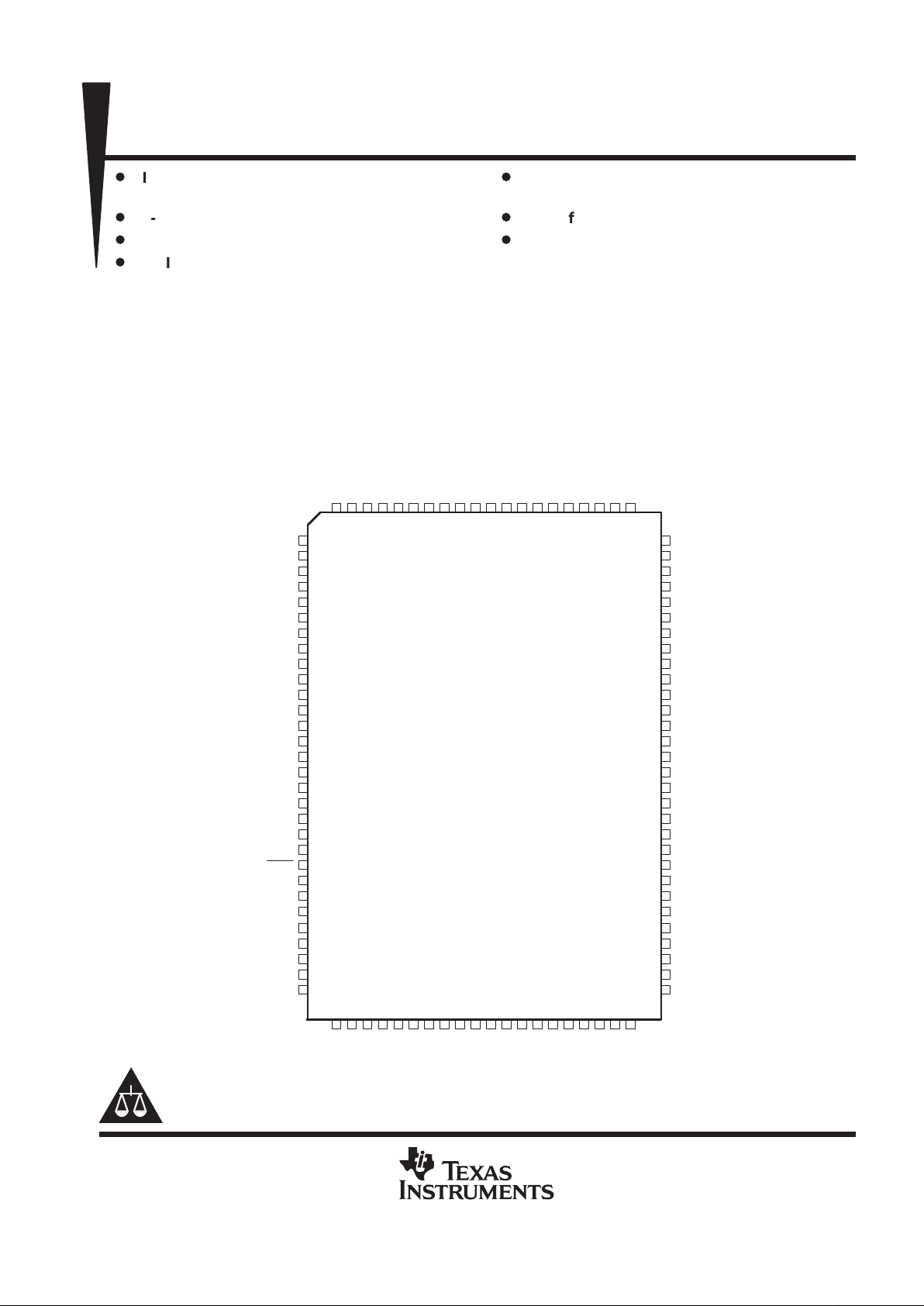
D
Interface to External ROM/EPROM
(Up to 8 MBytes)
D
8-Bit Microprocessor with 61 instructions
D
32 Twelve-Bit Words and 992 Bytes of RAM
D
4K Internal ROM
D
3.3V to 6.5V CMOS Technology for Low
Power Dissipation
D
28 Software-Configurable I/O Lines
D
10-kHz or 8-kHz Speech Sample Rate
description
The MSP50C30 combines an 8-bit microprocessor, two speech synthesizers, ROM, RAM, and I/O in a low-cost
single-chip system. The architecture uses the same arithmetic logic unit (ALU) for the two synthesizers and the
microprocessor, thus reducing chip area and cost and enabling the microprocessor to do a multiply operation
in 0.8 µs. The MSP50C30 features two independent channels of linear predictive coding (LPC), which
synthesize high-quality speech at a low data rate. Pulse-code modulation (PCM) can produce music or sound
effects. For more information, see the MSP50C30 User’s Guide (literature number SPSU012).
1
2
3
4
5
6
7
8
9
10
11
12
13
14
15
16
17
18
19
20
21
22
23
24
25
81
82
83
84
85
86
87
88
89
90
91
92
93
94
95
96
97
98
99
100
80
79
78
77
76
75
74
73
72
71
70
69
68
67
66
65
64
63
62
61
60
59
58
57
56
50
49
48
47
46
45
44
43
42
41
40
39
38
37
36
35
34
33
32
31
NC
NC
NC
NC
OA0
PD3
PD2
PD1
PD0
DAC–
DAC+
PC6
PC7
PC3
PC2
PC1
PC0
OSC OUT
NC
NC
NC
NC
NC
NC
OA17
OA18
OA19
OA21
OA22
ID7
ID6
ID5
ID4
ID3
ID2
ID1
ID0
PA0
NC
OA16
OA14
OA13
OA12
OA11
OA10
OA7
OA3
OA2
OA1NCNC
NC
PA1
PA2
PA3
PA4
PA5
PA6
NC
PA7
PB1
PB2
PB3
PB4
PB5
PB7
OSC IN
PB6
PJM PACKAGE
(TOP VIEW)
NC
OA5
OA9
OA8
NC
PC4
PB0
OA20
V
SS
INIT
26
27
28
29
30
55
54
53
52
51
NC
NC
NC
NC
NC
NC
NC
NC
NC
NC
OA4
OA15
V
DD
NC
NC
NC
PC5
V
SS
V
DD
NC
OA6
NC
Copyright 1998, Texas Instruments Incorporated
PRODUCTION DATA information is current as of publication date.
Products conform to specifications per the terms of Texas Instruments
standard warranty. Production processing does not necessarily include
testing of all parameters.
Please be aware that an important notice concerning availability, standard warranty, and use in critical applications of
Texas Instruments semiconductor products and disclaimers thereto appears at the end of this data sheet.
Page 2
MSP50C30
MIXED-SIGNAL PROCESSOR
SPSS021 NOVEMBER 1998
2
POST OFFICE BOX 655303 • DALLAS, TEXAS 75265
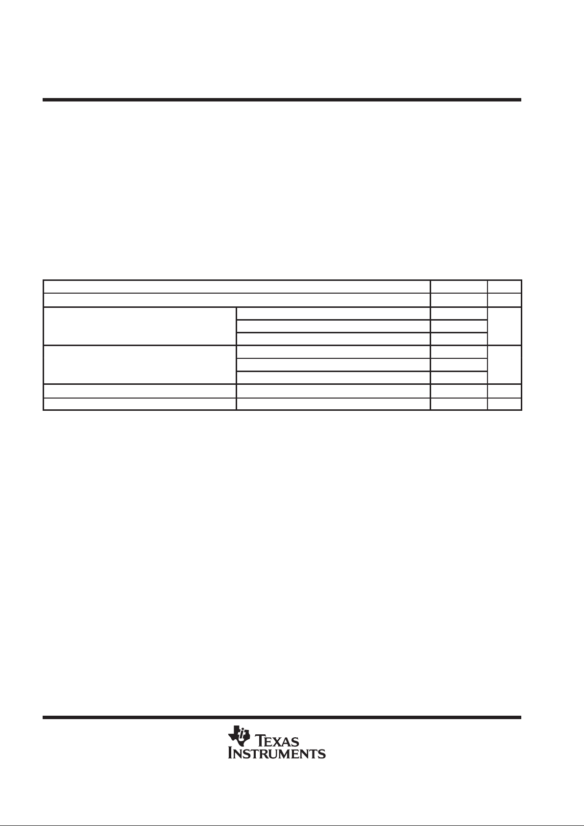
absolute maximum ratings over operating free-air temperature range
†
Supply voltage range, V
DD
(see Note 1) –0.3 V to 8 V. . . . . . . . . . . . . . . . . . . . . . . . . . . . . . . . . . . . . . . . . . . . . .
Supply current, I
DD
or ISS (see Note 2) 100 mA. . . . . . . . . . . . . . . . . . . . . . . . . . . . . . . . . . . . . . . . . . . . . . . . . . .
Input voltage range, V
I
(see Note 1) –0.3 V to VDD + 0.3 V. . . . . . . . . . . . . . . . . . . . . . . . . . . . . . . . . . . . . . . . . .
Output voltage range, V
O
(see Note 1) –0.3 V to VDD + 0.3 V. . . . . . . . . . . . . . . . . . . . . . . . . . . . . . . . . . . . . . .
Storage temperature range –30°C to 125°C. . . . . . . . . . . . . . . . . . . . . . . . . . . . . . . . . . . . . . . . . . . . . . . . . . . . . . .
†
Stresses beyond those listed under “absolute maximum ratings” may cause permanent damage to the device. These are stress ratings only, and
functional operation of the device at these or any other conditions beyond those indicated under “recommended operating conditions” is not
implied. Exposure to absolute-maximum-rated conditions for extended periods may affect device reliability.
NOTES: 1. All voltages are with respect to ground.
2. The total supply current includes the current out of all the I/O terminals and DAC terminals as well as the operating current of the
device.
recommended operating conditions (MSP50C32, MSP50C33, MSP50x34)
MAX MAX UNIT
V
DD
Supply voltage
†
3.3 6.5 V
VDD = 3.3 V 2.5 3.3
V
IH
High-level input voltage
VDD = 5 V
3.8 5
V
VDD = 6 V 4.5 6
VDD = 3.3 V 0 0.65
V
IL
Low-level input voltage
VDD = 5 V
0 1
V
VDD = 6 V 0 1.3
T
A
Operating free-air temperature Device functionality 0 70 °C
Rspeaker Minimum speaker impedance Direct speaker drive using 2 pin push-pull DAC option 32 Ω
†
Unless otherwise noted, all voltages are with respect to VSS.
Page 3
MSP50C30
MIXED-SIGNAL PROCESSOR
SPSS021 NOVEMBER 1998
3
POST OFFICE BOX 655303 • DALLAS, TEXAS 75265
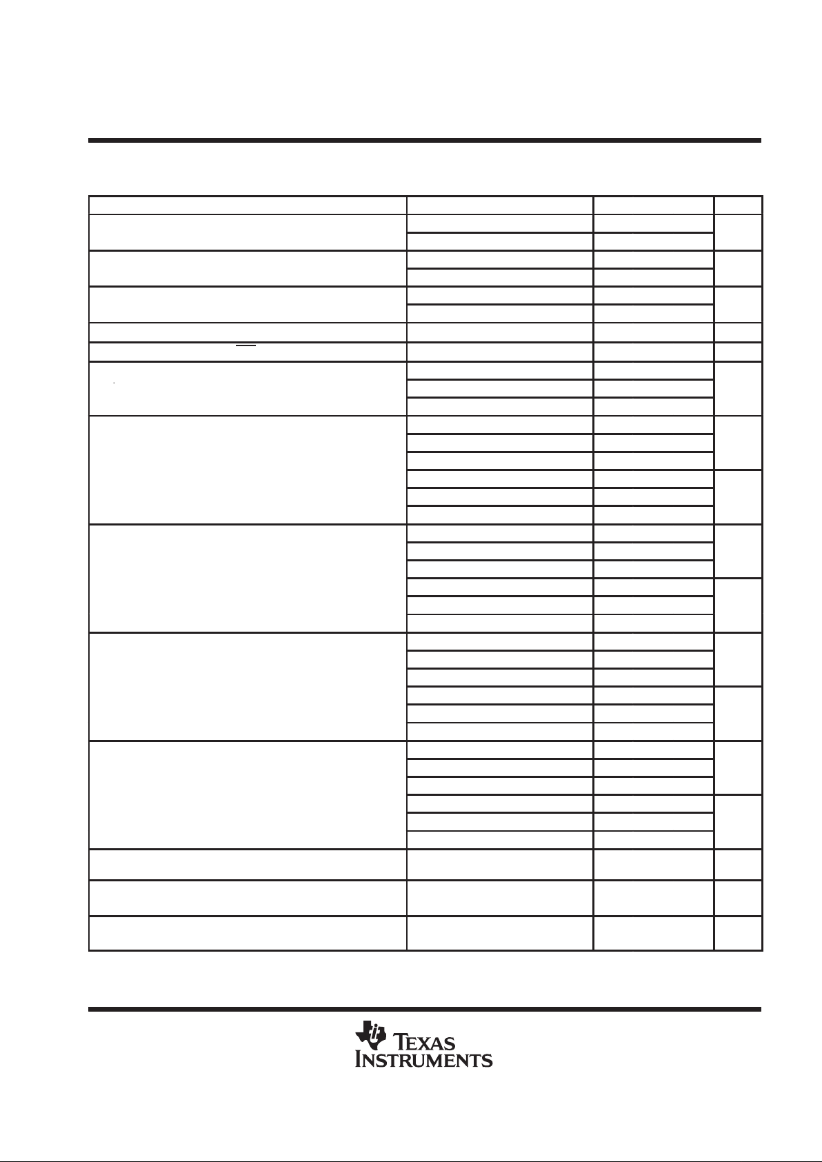
electrical characteristics over recommended ranges of supply voltage and operating free-air
temperature (unless otherwise noted)
PARAMETER TEST CONDITIONS MIN TYP MAX UNIT
VDD = 3.5 V 2
VT+Positive-going threshold voltage (INIT)
VDD = 6 V 3.4
V
VDD = 3.5 V 1.6
VT–Negative-going threshold voltage (INIT)
VDD = 6 V 2.3
V
VDD = 3.5 V 0.4
V
hys
Hysteresis (V
T+
–
VT–) (INIT)
VDD = 6 V 1.1
V
I
Ikg
Input leakage current (except for OSC IN)
2 µA
I
standby
Standby current (INIT low, SETOFF)
10 µA
VDD = 3.3 V, 2.1
I
DD
†
Supply current
VDD = 5 V,
3.1
mA
DD
VDD = 6 V, 4.5
VDD = 3.3 V, VOH = 2.75 V –4 –12
VDD = 5 V, VOH = 4.5 V –5 –14
mA
p
VDD = 6 V, VOH = 5.5 V –6 –15
IOHHigh-level output current (PA, PB)
VDD = 3.3 V, VOH = 2.2 V –8 –20
VDD = 5 V, VOH = 3.33 V –14 –40
mA
VDD = 6 V, VOH = 4 V –20 –51
VDD = 3.3 V, VOL = 0.5 V 5 9
VDD = 5 V, VOL = 0.5 V 5 9
mA
p
VDD = 6 V, VOL = 0.5 V 5 9
IOLLow-level output current (PA, PB)
VDD = 3.3 V, VOL = 1.1 V 10 19
VDD = 5 V, VOL = 1.67 V 20 29
mA
VDD = 6 V, VOL = 2 V 25 35
VDD = 3.3 V, VOH = 2.75 V –30 –50
VDD = 5 V, VOH = 4.5 V –35 –60
mA
p
VDD = 6 V, VOH = 5.5 V –40 –65
IOHHigh-level output current (D/A)
VDD = 3.3 V, VOH = 2.3 V –50 –90
VDD = 5 V, VOH = 4 V –90 –140
mA
VDD = 6 V, VOH = 5 V –100 –150
VDD = 3.3 V, VOL = 0.5 V 50 80
VDD = 5 V, VOL = 0.5 V 70 90
mA
p
VDD = 6 V, VOL = 0.5 V 80 110
IOLLow-level output current (D/A)
VDD = 3.3 V, VOL = 1 V 100 140
VDD = 5 V, VOL = 1 V 140
mA
VDD = 6 V, VOL = 1 V 150
Pullup resistance
Resistors selected by software and
connected between terminal and V
DD
10 20 50 kΩ
VDD = 5 V, TA = 25°C,
f
osc(low)
Oscill
ator frequency
‡
Target frequency = 15.36 MHz
14.89
15.36
15.86
MH
z
VDD = 5 V, TA = 25°C,
f
osc(high)
Oscill
ator frequency
‡
Target frequency = 19.2 MHz
18.62
19.2
19.7
MH
z
†
Operating current assumes all inputs are tied to either VSS or VDD with no input currents due to programmed pullup resistors. The DAC output
and other outputs are open circuited.
‡
The frequency of the internal clock has a temperature coefficient of approximately –0.2 %/°C and a VDD coefficient of approximately ±1%/V.
Page 4

MSP50C30
MIXED-SIGNAL PROCESSOR
SPSS021 NOVEMBER 1998
4
POST OFFICE BOX 655303 • DALLAS, TEXAS 75265
switching characteristics
PARAMETER TEST CONDITIONS MIN NOM MAX UNIT
t
Rise time
PA, PB, PC,
PD, D/A
VDD = 3.3 V, CL = 100 pF, 10% to 90%
50
ns
t
r
Rise time
OA
VDD = 3.3 V, CL = 50 pF, 10% to 90%
50
ns
t
Fall time
PA, PB, PC,
PD, D/A
VDD = 3.3 V, CL = 100 pF, 10% to 90%
50
ns
t
f
Fall time
OA
VDD = 3.3 V, CL = 50 pF, 10% to 90%
50
ns
timing requirements
MIN MAX UNIT
Initialization
t
INIT
INIT pulsed low while the MSP50x3x has power applied (see Figure 1)
1 µs
Wakeup
t
su(wakeup)
Setup time prior to wakeup terminal negative transition (see Figure 2)
1 µs
External Interrupt
f
clock
= 15.36 MHz 1
t
su(interrupt)
Set
up time prior to B1 terminal negative trans
iti
on (see Figure
3)
f
clock
= 19.2 MHz 1.5
µ
s
Writing (Slave Mode)
t
su1(B1)
Setup time, B1 low before B0 goes low (see Figure 4) 20 ns
t
su(d)
Setup time, data valid before B0 goes high (see Figure 4) 100 ns
t
h1(B1)
Hold time, B1 low after B0 goes high (see Figure 4) 20 ns
t
h(d)
Hold time, data valid after B0 goes high (see Figure 4) 30 ns
t
w
Pulse duration, B0 low (see Figure 4) 100 ns
t
r
Rise time, B0 (see Figure 4) 50 ns
t
f
Fall time, B0 (see Figure 4) 50 ns
Reading (Slave Mode)
t
su2(B1)
Setup time, B1 before B0 goes low (see Figure 5) 20 ns
t
h2(B1)
Hold time, B1 after B0 goes high (see Figure 5) 20 ns
t
dis
Output disable time, data valid after B0 goes high (see Figure 5) 0 30 ns
t
w
Pulse duration, B0 low (see Figure 5) 100 ns
t
r
Rise time, B0 (see Figure 5) 50 ns
t
f
Fall time, B0 (see Figure 5) 50 ns
t
d
Delay time for B0 low to data valid (see Figure 5) 50 ns
External ROM
t
a(ROM)
ROM access time 400 ns
Page 5

MSP50C30
MIXED-SIGNAL PROCESSOR
SPSS021 NOVEMBER 1998
5
POST OFFICE BOX 655303 • DALLAS, TEXAS 75265
PARAMETER MEASUREMENT INFORMATION
t
INIT
INIT
Figure 1. Initialization Timing Diagram
t
su(wakeup)
Wakeup
Figure 2. Wakeup Terminal Setup Timing Diagram
t
su(interrupt)
B1
Figure 3. External Interrupt Terminal Setup Timing Diagram
Data Valid
B1
B0
PA
t
su1(B1)
t
w
t
h1(B1)
t
f
t
su(d)
t
r
t
h(d)
Figure 4. Write Timing Diagram (Slave Mode)
Page 6

MSP50C30
MIXED-SIGNAL PROCESSOR
SPSS021 NOVEMBER 1998
6
POST OFFICE BOX 655303 • DALLAS, TEXAS 75265
PARAMETER MEASUREMENT INFORMATION
Data Valid
B1
B0
PA
t
su2(B1)
t
w
t
h2(B1)
t
f
t
r
t
dis
t
d
Figure 5. Read Timing Diagram (Slave Mode)
Page 7

MSP50C30
MIXED-SIGNAL PROCESSOR
SPSS021 NOVEMBER 1998
7
POST OFFICE BOX 655303 • DALLAS, TEXAS 75265
MECHANICAL DATA
PJM (R-PQFP-G100) PLASTIC QUAD FLATPACK
4040022/B 03/95
0,16 NOM
14,20 17,45
13,80 16,95
50
51
31
30
12,35 TYP
1,03
0,73
0,25
Seating Plane
0,25 MIN
Gage Plane
0,38
0,22
80
1
81
100
22,95
23,45
20,20
19,80
2,50
2,90
3,40 MAX
18,85 TYP
0°–7°
M
0,13
0,65
0,10
NOTES: A. All linear dimensions are in millimeters.
B. This drawing is subject to change without notice.
C. Falls within JEDEC MS-022
Page 8

IMPORTANT NOTICE
T exas Instruments and its subsidiaries (TI) reserve the right to make changes to their products or to discontinue
any product or service without notice, and advise customers to obtain the latest version of relevant information
to verify, before placing orders, that information being relied on is current and complete. All products are sold
subject to the terms and conditions of sale supplied at the time of order acknowledgement, including those
pertaining to warranty, patent infringement, and limitation of liability.
TI warrants performance of its semiconductor products to the specifications applicable at the time of sale in
accordance with TI’s standard warranty. Testing and other quality control techniques are utilized to the extent
TI deems necessary to support this warranty. Specific testing of all parameters of each device is not necessarily
performed, except those mandated by government requirements.
CERT AIN APPLICATIONS USING SEMICONDUCTOR PRODUCTS MAY INVOLVE POTENTIAL RISKS OF
DEATH, PERSONAL INJURY, OR SEVERE PROPERTY OR ENVIRONMENTAL DAMAGE (“CRITICAL
APPLICATIONS”). TI SEMICONDUCTOR PRODUCTS ARE NOT DESIGNED, AUTHORIZED, OR
WARRANTED TO BE SUITABLE FOR USE IN LIFE-SUPPORT DEVICES OR SYSTEMS OR OTHER
CRITICAL APPLICATIONS. INCLUSION OF TI PRODUCTS IN SUCH APPLICA TIONS IS UNDERST OOD TO
BE FULLY AT THE CUSTOMER’S RISK.
In order to minimize risks associated with the customer’s applications, adequate design and operating
safeguards must be provided by the customer to minimize inherent or procedural hazards.
TI assumes no liability for applications assistance or customer product design. TI does not warrant or represent
that any license, either express or implied, is granted under any patent right, copyright, mask work right, or other
intellectual property right of TI covering or relating to any combination, machine, or process in which such
semiconductor products or services might be or are used. TI’s publication of information regarding any third
party’s products or services does not constitute TI’s approval, warranty or endorsement thereof.
Copyright 1998, Texas Instruments Incorporated
 Loading...