

Page 1

CLC520
CLC520 Amplifier with Voltage Controlled Gain, AGC +Amp
Literature Number: SNOS861C
Page 2
CLC520
Amplifier with Voltage Controlled Gain, AGC +Amp
CLC520 Amplifier with Voltage Controlled Gain, AGC +Amp
May 2001
General Description
The CLC520 is a wideband DC-coupled amplifier with voltage controlled gain (AGC). The amplifier has a high impedance, differential signal input; a high bandwidth, gain control
input; and a single-ended voltage output. Signal channel
performance is outstanding with 160MHz small signal bandwidth, 0.5 degree linear phase deviation (to 60MHz) and
0.04% signal nonlinearity at 4V
Gain control is very flexible and easy to use. Maximum gain
may be set over a nominal range of 2 to 100 with one
external resistor. In addition, the gain control input provides
more than 40dB of voltage controlled gain adjustment from
the maximum gain setting. For example, a CLC520 may be
set for a maximum gain of 2 (or 6dB) for a voltage controlled
gain range from 40dB to less than 34dB. Alternatively, the
CLC520 could be set for a maximum gain of 100 or (40dB)
for a voltage controlled gain range from 40dB to less than
0dB.
The gain control bandwidth of 100MHz is superb for AGC/
ALC loop stabilization. And since the gain is minimum with a
zero volt input and maximum with a +2 volt input, driving the
control input is easy.
Finally, the CLC520 differential inputs, and ground referenced voltage output take the trouble out of designing
DC-coupled AGC circuits for display normalizers; signal leveling automatic circuits; etc.
Enhanced Solutions (Military/Aerospace)
SMD Number: 5962-91694
Space level versions also available.
For more information, visit http://www.national.com/mil
PP
output.
Features
n 160MHz, −3dB bandwidth
n 2000V/µsec slew rate
n 0.04% signal nonlinearity at 4V
n −43dB feedthrough at 30MHz
n User adjustable gain range
n Differential voltage input and single-ended voltage
output
PP
output
Applications
n Wide bandwidth AGC systems
n Automatic signal leveling
n Video signal processing
n Voltage controlled filters
n Differential amplifier
n Amplitude modulation
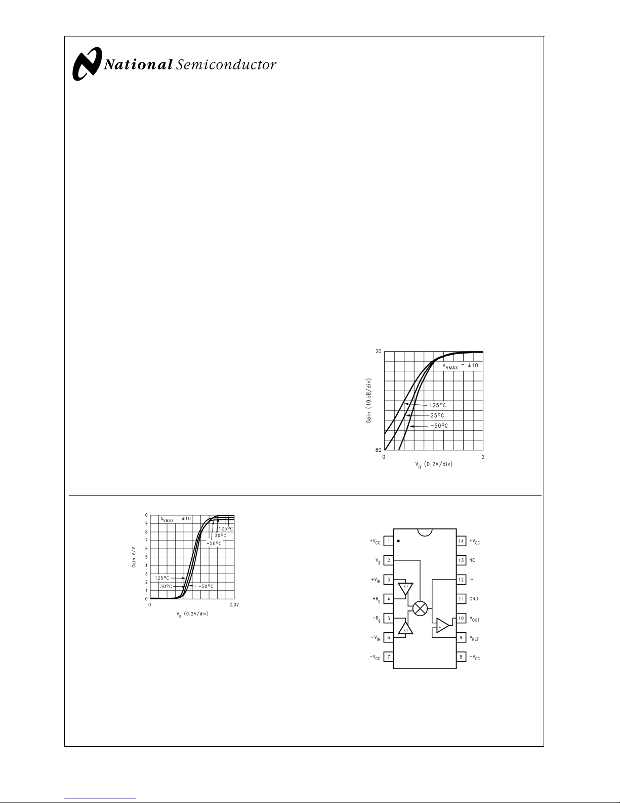
Gain vs. V
g
01275640
Gain vs. V
© 2001 National Semiconductor Corporation DS012756 www.national.com
g
Connection Diagram
01275639
01275629
Pinout
DIP & SOIC
Page 3

Ordering Information
CLC520
Package Temperature Range
Industrial
14-pin plastic DIP −40˚C to +85˚C CLC520AJP CLC520AJP N14A
14-pin plastic SOIC −40˚C to +85˚C CLC520AJE CLC520AJE M14A
Part Number Package
Marking
NSC
Drawing
www.national.com 2
Page 4
CLC520
Absolute Maximum Ratings (Note 1)
If Military/Aerospace specified devices are required,
please contact theNationalSemiconductor Sales Office/
Distributors for availability and specifications.
Supply Voltage (V
I
OUT
Output is short circuit protected to
ground, but maximum reliability will
be maintained if I
exceed... 60mA
Common Mode Input Voltage
VINDifferential Input Voltage 10V
V
Differential Input Voltage
g
V
Differential Input Voltage
ref
CC
OUT
)
does not
±
7V
±
V
CC
±
V
CC
±
V
CC
Junction Temperature +150˚C
Operating Temperature Range −40˚C to +85˚C
Storage Temperature Range −65˚C to +150˚C
Lead Solder Duration (+300˚C) 10 sec
ESD (human body model) 500V
Operating Ratings
Thermal Resistance
Package (θ
MDIP 55˚C/W 105˚C/W
SOIC 45˚C/W 120˚C/W
)(θ
JC
)
JA
Electrical Characteristics
AV= +10, VCC=±5V, RL= 100Ω,Rf=1kΩ,Rg= 182Ω,Vg= +2V; unless specified
Symbol Parameter Conditions Typ Max/Min (Note 2) Units
Ambient Temperature CLC520AJ +25˚C −40˚C +25˚C +85˚C
Frequency Domain Response
SSBW -3dB Bandwidth V
SSBW V
LSBW V
-3dB Bandwidth V
SBWC Gain Control Channel VIN= +0.2V, Vg= +1VDC 100
Gain Flatness V
GFPL Peaking 0.1MHz to 30MHz 0
GFPH Peaking 0.1MHz to 20MHz 0
GFRL Rolloff 0.1MHz to 30MHz 0.1
GFRH Rolloff 0.1MHz to 60MHz 0.5
LPD Linear Phase Deviation 0.1MHz to 60MHz 0.5
FDTH Feedthrough V
TRS Rise and Fall Time 0.5V Step 2.5
TRL 4.0V Step 3.7
TS Settling Time to
OS Overshoot 0.5V Step 0
SR Slew Rate 4V Step 2000
HD2 2nd Harmonic Distortion 2V
HD3 3rd Harmonic Distortion 2V
Equivalent Output Noise (÷10 for input noise) (Note
SNF Noise floor 1MHz to 200MHz −132
INV Integrated noise 1MHz to 200MHz 800
DG Differential Gain (Note 4) at 3.58MHz 0.15 %
DP Differential PIase (Note 4) at 3.58MHz 0.15 deg
Static, DC Performance
SGNL Integral Signal Nonlinearity V
Gain Accuracy R
GACCU For Nominal Max Gain = 20dB
VOS Output Offset Voltage (Note 5) 40
DVOS Average Temperature Coefficient 100
±
0.1% 2.0V Step 12
<
0.5V
OUT
OUT
OUT
OUT
OUT
= 0V, VIN= -22dBm -38
g
PP
PP
3)
OUT
=1kΩ,Rg= 182Ω
f
PP
<
0.5VPP(AJE only) 140
<
4.0V
PP
<
0.5V
PP
<
0.5V
PP
, 20MHz −47
, 20MHz −60
=4V
PP
160
140
0.04
±
0
>
110
>
90
>
85
>
80
<
0.4
<
0.7
<
0.4
<
1.3
<
1.2
<
-31
<
3.7
<
5
<
18
<
15
>
1450
<
−40
<
−50
<
−130
<
1000
<
0.1
<
±
1.0
<
150
<
400 –
>
>
>
<
<
<
<
>
<
<
<
<
<
<
<
120
100
100
>
80
0.3
0.5
0.3
<
1
<
1
-31
<
3
<
5
<
18
<
15
1450
−40
−50
−130
1000
0.1
±
0.5
120
>
120 MHz
>
100 MHz
>
100 MHz
>
80 MHz
<
0.4 dB
<
0.7 dB
<
0.4 dB
<
1.3 dB
<
1.2 deg
<
-31 dB
<
3ns
<
5ns
<
18 ns
<
15 %
>
1450 V/µsec
<
−35 dBc
<
−45 dBc
<
−129 dBm
(1Hz)
<
1100 µV
<
0.2 %
<
±
0.5 dB
<
150 mV
<
300 µV/˚C
www.national.com3
Page 5
Electrical Characteristics (Continued)
AV= +10, VCC=±5V, RL= 100Ω,Rf=1kΩ,Rg= 182Ω,Vg= +2V; unless specified
CLC520
Symbol Parameter Conditions Typ Max/Min (Note 2) Units
IB Input Bias Current (Note 5) 12
DIB Average Temperature Doefficient 100
IOS Input Offset Current 0.5
DIOS Average Temperature Coefficient 5
PSS Power Supply Sensitivity Output Referred DC 10
CMRR Common Mode Rejection Ratio Input Referred 70
ICC Supply Current (Note 5) No Load 28
RIN V
CIN Capacitance 1
DMIR V
CMIR Common Mode Voltage Range
RINC V
CINC Capacitance 1
VGHI V
VGLO For Min Gain 0.4
RO Output Impedance At DC 0.1
VO Output Voltage Range No Load
IO Output Current
Note 1: “Absolute Maximum Ratings” are those values beyond which the safety of the device cannot be guaranteed. They are not meant to imply that the devices
should be operated at these limits. The table of “Electrical Characteristics” specifies conditions of device operation.
Note 2: Max/min ratings are based on product characterization and simulation. Individual parameters are tested as noted. Outgoing quality levels are determined
from tested parameters.
Note 3: Measured at A
Note 4: Differential gain and phase are measured at: A
at 3.58 MHz.
Note 5: AJ-level: spec. is 100% tested at +25˚C.
Signal Input Resistance 200
IN
Differential Voltage Range Rg= 182Ω only
IN
Control Input Resistance 750
g
Input Voltage For Max Gain 1.6
g
= 10, Vg= +2V
VMAX
= +20, Vg= +2V, RL= 150Ω,Rf=2kΩ,Rg= 182Ω, equivalent video signal of 0-100 IRE with 40 IRE
V
±
280
±
2.2
±
3.5
±
60
<
61
<
415 -
<
4
<
40 -
<
28
>
59
<
38
>
50
<
2
±
250
>
±
1.4
>
535
<
2
<
2
>
0
<
0.3
>
±
3
>
±
35
<
28
<
2
<
28
>
59
<
38
>
100
<
2
±
250
>
±
2
>
600
<
2
<
2
>
0
<
0.2
>
±
3.2
>
±
50
<
28 µA
<
165 nA/˚C
<
2µA
<
20 nA/˚C
<
28 mV/V
>
59 dB
<
38 mA
>
100 kΩ
<
2pF
±
210 mV
>
±
2V
>
600 Ω
<
2pF
<
2kΩ
>
0V
<
0.2 Ω
>
±
3.2 V
>
±
50 mA
PP
www.national.com 4
Page 6

Typical Performance Characteristics
(TA= 25˚C, AV= +10, VCC=±5V, RL= 100Ω,Rf=
1kΩ,R
= 182Ω,Vg= +2V)
g
CLC520
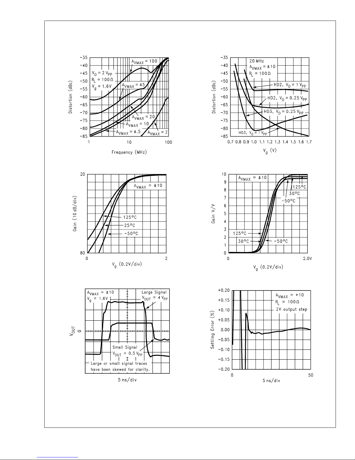
Frequency Response, A
Frequency Response, A
=±2 Frequency Response, A
VMAX
01275630 01275616
=±100 Large Signal Frequency Response
VMAX
VMAX
=±10
Small Signal Gain vs. R
01275619 01275621
f
01275641
2nd Harmonic Distortion
01275601
www.national.com5
Page 7
Typical Performance Characteristics (T
= 182Ω,Vg= +2V) (Continued)
CLC520
3rd Harmonic Distortion 2nd and 3rd Harmonic Distortion vs. V
= 25˚C, AV= +10, VCC=±5V, RL= 100Ω,Rf=1kΩ,R
A
g
g
01275602
Gain vs. V
g
01275640
Gain vs. V
g
Large and Small Signal Pulse Response Settling Time, Vg=2V
01275603
01275639
www.national.com 6
01275642
01275613
Page 8

CLC520
Typical Performance Characteristics (T
= 182Ω,Vg= +2V) (Continued)
Settling Time, V
Settling Time vs. Capacitive Load, A
= 1.2V Long-Term Settling Time
g
01275614
=±10 Gain Control Settling Time
VMAX
= 25˚C, AV= +10, VCC=±5V, RL= 100Ω,Rf=1kΩ,R
A
01275615
g
01275604
Gain Control Channel Feedthrough CMRR
01275618
01275617
01275605
www.national.com7
Page 9

Typical Performance Characteristics (T
= 182Ω,Vg= +2V) (Continued)
CLC520
Differential Gain and Phase PSRR
= 25˚C, AV= +10, VCC=±5V, RL= 100Ω,Rf=1kΩ,R
A
g
01275643
Output Noise vs. V
g
01275622
Linearity, Vg= 0.6V to 1.6V
Linearity, Vg= 0.75V to 1.4V Linearity, Vg= 0.9V to 1.2V
01275606
01275644
www.national.com 8
01275645 01275646
Page 10

Application Information
01275607
FIGURE 1. CLC520 Simplified Schematic
Simplified Circuit Description
A simplified schematic for the CLC520 is given in
+V
and −VINare buffered with closed-loop voltage follow-
IN
ers inducing a signal current in R
(+V
)−(−VIN), the differential input voltage. This current con-
IN
g
trols a current source which supplies two well matched transistors, Q1 and Q2.
The current flowing through Q2 is converted to the final
output voltage using R
and output amplifier, U1. By chang-
f
ing the fraction of the signal current I which flows through Q2
the gain is changed. This is done by changing the voltage
applied differentially to the bases of Q1 and Q2. For example, with V
current of flowing through Q2 into R
minimum gain. Conversely, with V
the signal current I flows through Q2 to R
mum gain. With V
= 0, Q1 is on and Q2 is off. With zero signal
g
set to 1.1V, the bases of Q1 and Q2 are
g
, the CLC520 is set to
f
= 2V, Q1 is off and all of
g
f
set to approximately the same voltage, causing their collector currents to equally divide the signal current I, and establish the gain at one half the maximum gain.
Typical application circuit
Figure 2
illustrates a voltage-controlled gain block offering
broadband performance in a 50Ω system environment. The
input signal is applied to pin 3 of the CLC520 and terminating
resistor R2. Gain control signals are applied to pin 2. The net
gain control port input impedance is 50Ω, set by the parallel
combination of R1 and the 750Ω input impedance of pin 2 of
the CLC520. R
is set to the standard value, 1kΩ, and R
f
sets the maximum voltage gain to 10V/V. Output impedance
is set by R
to 50Ω so with 50Ω source and load termina-
o
tions, the gain is approximately 14dB.
Figure 1
proportional to
producing maxi-
CLC520
.
01275608
FIGURE 2. CLC520 Typical Application Circuit
Capacitors C1-C6 provide broadband power supply bypassing. C2 and C5 should be tantalum capacitors. All other
capacitors should be high quality ceramic capacitors (CK-05
or equivalent).
Adjusting offset
Offset can be broken into two parts; an input-referred term
and an output-referred term. The input-referred offset shows
up as a variation in output voltage as V
be trimmed using the circuit in
frequency square wave (V
the input referred V
os
riding a DC value.Adjust R
= 0 to 2V, into Vgwith VIN=0V,
IN
term shows up as a small square wave
to null the Vossquare wave term
1
to zero. After adjusting the input-referred offset, adjust R2
(with V
applications V
=0,Vg= 0) until V
IN
may be applied to pin 6 and the offset
IN
OUT
adjustment to pin 3. This offset trim does not improve output
offset temperature coefficient.
g
is changed. This can
g
Figure 3
by placing a low
is zero. Finally, for inverting
01275628
FIGURE 3. CLC520 Offset Adjustment Circuitry
(other external elements not shown)
Selecting component values
Most applications of the CLC520 adjust the gain to maximize
the V
signal. When referred back to the input, this means
OUT
www.national.com9
Page 11
Application Information (Continued)
the input signal, signal-to-noise ratio is maximized. The
CLC520
maximum allowed input amplitude and from system specifications, using maximum required gain R
calculated.
The output stage op amp is a current-feedback type amplifier
optimized for R
=1kΩ.Rgcan then be computed as:
f
To determine whether the maximum input amplitude will
overdrive the CLC520, compute:
V
=(Rg+3.0Ω) · 0.00135
dmax
the maximum differential input voltage for linear operation. If
the maximum input amplitude exceeds the above V
then CLC520 should either be moved to a location in the
signal chain where input amplitudes are reduced, or the
CLC520 gain A
should be reduced or the values for R
VMAX
and Rfshould be increased. The overall system performance
impact is different based on the choice made.
If the input amplitude is reduced, recompute the impact on
signal-to-noise ratio. If A
VMAX
is reduced,
and Rgcan be
f
dmax
limit,
capacitance across the feedback resistor should not be used
to compensate for this effect.
<
For best performance at low maximum gains (A
R
+ and Rgconnections should be treated in a similar fash-
g
VMAX
10)
ion. Capacitance to ground should be minimized by removing the ground plane from under the resistor of R
.
g
Parasitic or load capacitance directly on the output (pin 10)
degrades phase margin leading to frequency response
peaking. A small series resistor before this capacitance,
effectively reduces this effect (see Settling Time vs. Capacitive Load).
Precision buffed resistors (PRP8351 series from Precision
Resistive Products) must be used for R
mance. Precision buffed resistors are suggested for R
low gain settings (A
<
10). Carbon composition resis-
VMAX
for rated perfor-
f
for
g
tors and RN55D metal-film resistors may be used with reduced performance.
Evaluation PC boards (part no. 730021) for the CLC520 are
available.
Predicting the output noise
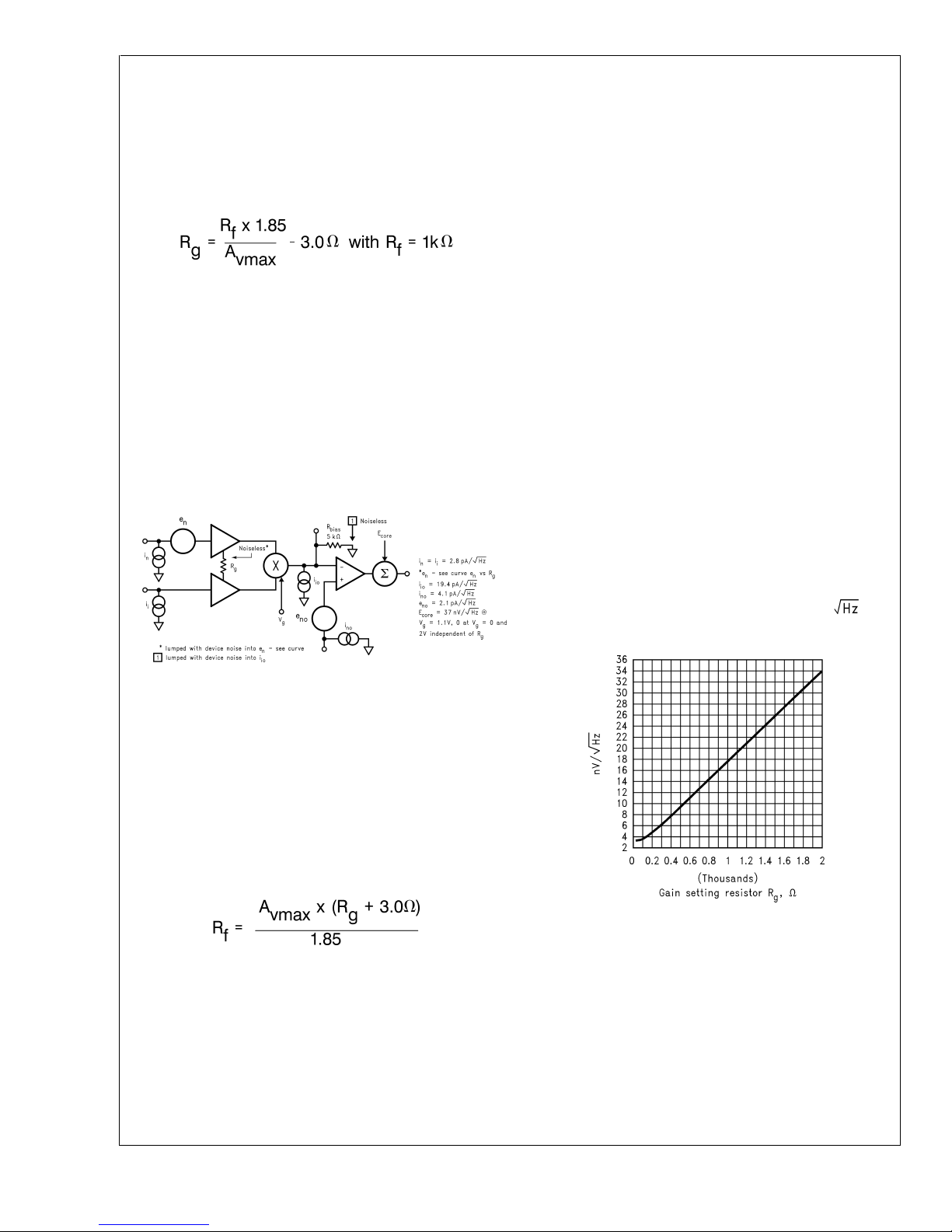
g
Seven noise sources (e
model the CLC520 noise performance (
i
model the equivalent input noise terms for the input buffer
i
while i
, and enomodel the noise terms for the output
io,ino
buffer.To simplify the model e
R
(see
Figure 5
g
R
is assumed noiseless and its noise contribution is
bias
included in i
.
io
An additional term E
n,in,ii,iio,ino,eno,Ecore
includes the effect of resistor
n
for envs. Rg). To simplify the model further,
mimics the active device noise
core
Figure 4
) are used to
). en,in, and
contribution from the Gilbert multiplier core. Core noise is
theoretically zero when the multiplier is set to maximum gain
or zero gain (V
>
1.6V or V
g
temperature) and reaches a maximum of 37nV/
A
/2.
VMAX
<
0.63V respectively at room
g
at
01275647
FIGURE 4. CLC520 Noise Model
Post CLC520 amplifier gain, should be increased, or another
gain stage added to make up for reduced system gain..
To increase R
and Rf, where V
g
= (+VIN)−(−VIN) the
dmax
largest expected peak differential input voltage. Compute the
lowest acceptable value for R
>
R
740˚V
g
Operating with R
−3Ω
dmax
larger than this value insures linear op-
g
:
g
eration of the input buffers.
R
may be computed from selected Rgand A
f
VMAX
:
Rfshould be>=1kΩfor overall best performance, however
<
R
1kΩ can be implemented if necessary using a loop gain
f
reducing resistor to ground on the inverting summing node of
the output amplifier (see application note QA-13 for details).
Printed Circuit Layout
A good high frequency PCB layout including ground plane
construction and power supply bypassing close to the package are critical to achieving full performance. The amplifier is
sensitive to stray capacitance to ground at the
Inverting-input (pin12); keep node trace area small. Shunt
01275648
FIGURE 5. Equivalent Input Noise Voltage (en) vs. R
g
Several points should be made concerning this model. First,
external component noise contributions need to be factored
in when computing total output referred noise. The only
exception is R
, where its noise contribution is already fac-
g
tored in. Second, the model ignores flicker noise contributions.Applications where noise below approximately 100kHz
must be considered should use this model with caution.
Third, this model very accurately predicts output noise voltage for the typical application circuit (see above) but accuracy will degrade the component values deviate further from
those in the typical application circuit. In general, however,
www.national.com 10
Page 12

Application Information (Continued)
the model should predict the equivalent output noise above
the flicker noise region to within a few dB of actual performance over the normal range of A
values.
and component
VMAX
01275610
inodoes not contribute to the output buffer noise because the
output buffer non-inverting input is grounded.
The core noise is already output referred and is 37nV/
at Vg=1.1 (A
A
Summing the noise power for each term gives the
VMAX
/2) and approaches zero as A goes to 0 or
VMAX
total output noise power.
The total output noise voltage is given by:
CLC520
FIGURE 6. Typical Circuit
01275611
FIGURE 7. Noise Model for Typical Circuit
Calculating CLC520 output noise in a typical circuit
To calculate the noise in a CLC520 application, the noise
terms given for the amplifier as well as the noise terms of the
external components must be included. To clarify the techniques used, output noise in a typical circuit will be calculated. (
Figure 6
The noise model is depicted in
sumes spot noise source with V
)
Figure 7
rms
. The diagram as-
/ and Amps
rms
/
units. The Thevenin equivalent of the source and input termination is used; 25Ω in series with a noise voltage source.
R
is assumed noiseless since its effect is included in en.
g
The internal 5kΩ resistor at the CLC520 core output is also
assumed noiseless since its effect is included in i
noise contribution from R
is modeled as a noise source.
f
, The
io
The easiest way to analyze the output noise of this circuit is
to divide the noise power into three pieces; −input buffer
noise calculation, output buffer noise and core noise. The
input buffer varies with the gain. The output buffer term is
constant. The core noise term is zero at both maximum and
minimum gain and reaches peak at A
VMAX
/2.
Since we assume all noise terms are uncorrelated, the
equivalent input noise voltage squared is given by:
iidoes not contribute to the output buffer noise because the
input buffer inverting input is grounded. e
Figure 5
.
is taken from
n
The equivalent output buffer noise is given by:
Where AVis the input to output voltage gain, which varies
with V
.
g
C accounts for the variation in core noise contribution as V
is adjusted. C=1 when gain AVis A
A
and AV= 0 and varies between 0 and 1 for all other
VMAX
/2. C is zero at
VMAX
values.
Using these equations, total calculated output noise for the
circuit was 20nV/
mid-gain, and 53nV/
at minimum gain, 49nV/ at
at maximum gain.
01275612
FIGURE 8. Automatic Gain Control (AGC) Loop
AGC circuits
Figure 8
shows a typical AGC circuit. The CLC520 is followed up with a CLC401 for higher overall gain. The output
of the CLC401 is rectified and fed to an inverting integrator
using a CLC420 (wideband voltage feedback op amp).
When the output voltage, V
, is too large the integrator
OUT
output voltage ramps down reducing the net gain of the
CLC520 and V
. If the output voltage is too small, the
OUT
integrator ramps up increasing the net gain and the output
voltage.Actual output level is set with R1. To prevent shifts in
DC output voltage with DC changes in input signal level, trim
pot R2 is provided. AGC circuits are always limited in the
range of input signals over which constant output level can
be maintained. In this circuit, we would expect that reasonable AGC action could be maintained over the gain adjustment range of the CLC520 (at least 40dB). In practice,
rectifier dynamic range limits reduce this slightly.
Evaluation Board
Evaluation PC boards (part number 730029 for through-hole
and 730023 for SOIC) for the CLC520 are available.
g
www.national.com11
Page 13

Physical Dimensions inches (millimeters)
unless otherwise noted
CLC520
14-Pin MDIP
NS Package Number N14A
www.national.com 12
14-Pin SOIC
NS Package Number M14A
Page 14

Notes
CLC520 Amplifier with Voltage Controlled Gain, AGC +Amp
LIFE SUPPORT POLICY
NATIONAL’S PRODUCTS ARE NOT AUTHORIZED FOR USE AS CRITICAL COMPONENTS IN LIFE SUPPORT
DEVICES OR SYSTEMS WITHOUT THE EXPRESS WRITTEN APPROVAL OF THE PRESIDENT AND GENERAL
COUNSEL OF NATIONAL SEMICONDUCTOR CORPORATION. As used herein:
1. Life support devices or systems are devices or
systems which, (a) are intended for surgical implant
into the body, or (b) support or sustain life, and
whose failure to perform when properly used in
accordance with instructions for use provided in the
labeling, can be reasonably expected to result in a
significant injury to the user.
National Semiconductor
Corporation
Americas
Email: support@nsc.com
www.national.com
National does not assume any responsibility for use of any circuitry described, no circuit patent licenses are implied and National reserves the right at any time without notice to change said circuitry and specifications.
National Semiconductor
Europe
Email: europe.support@nsc.com
Deutsch Tel: +49 (0) 69 9508 6208
English Tel: +44 (0) 870 24 0 2171
Français Tel: +33 (0) 1 41 91 8790
Fax: +49 (0) 180-530 85 86
2. A critical component is any component of a life
support device or system whose failure to perform
can be reasonably expected to cause the failure of
the life support device or system, or to affect its
safety or effectiveness.
National Semiconductor
Asia Pacific Customer
Response Group
Tel: 65-2544466
Fax: 65-2504466
Email: ap.support@nsc.com
National Semiconductor
Japan Ltd.
Tel: 81-3-5639-7560
Fax: 81-3-5639-7507
Page 15

IMPORTANT NOTICE
Texas Instruments Incorporated and its subsidiaries (TI) reserve the right to make corrections, modifications, enhancements, improvements,
and other changes to its products and services at any time and to discontinue any product or service without notice. Customers should
obtain the latest relevant information before placing orders and should verify that such information is current and complete. All products are
sold subject to TI’s terms and conditions of sale supplied at the time of order acknowledgment.
TI warrants performance of its hardware products to the specifications applicable at the time of sale in accordance with TI’s standard
warranty. Testing and other quality control techniques are used to the extent TI deems necessary to support this warranty. Except where
mandated by government requirements, testing of all parameters of each product is not necessarily performed.
TI assumes no liability for applications assistance or customer product design. Customers are responsible for their products and
applications using TI components. To minimize the risks associated with customer products and applications, customers should provide
adequate design and operating safeguards.
TI does not warrant or represent that any license, either express or implied, is granted under any TI patent right, copyright, mask work right,
or other TI intellectual property right relating to any combination, machine, or process in which TI products or services are used. Information
published by TI regarding third-party products or services does not constitute a license from TI to use such products or services or a
warranty or endorsement thereof. Use of such information may require a license from a third party under the patents or other intellectual
property of the third party, or a license from TI under the patents or other intellectual property of TI.
Reproduction of TI information in TI data books or data sheets is permissible only if reproduction is without alteration and is accompanied
by all associated warranties, conditions, limitations, and notices. Reproduction of this information with alteration is an unfair and deceptive
business practice. TI is not responsible or liable for such altered documentation. Information of third parties may be subject to additional
restrictions.
Resale of TI products or services with statements different from or beyond the parameters stated by TI for that product or service voids all
express and any implied warranties for the associated TI product or service and is an unfair and deceptive business practice. TI is not
responsible or liable for any such statements.
TI products are not authorized for use in safety-critical applications (such as life support) where a failure of the TI product would reasonably
be expected to cause severe personal injury or death, unless officers of the parties have executed an agreement specifically governing
such use. Buyers represent that they have all necessary expertise in the safety and regulatory ramifications of their applications, and
acknowledge and agree that they are solely responsible for all legal, regulatory and safety-related requirements concerning their products
and any use of TI products in such safety-critical applications, notwithstanding any applications-related information or support that may be
provided by TI. Further, Buyers must fully indemnify TI and its representatives against any damages arising out of the use of TI products in
such safety-critical applications.
TI products are neither designed nor intended for use in military/aerospace applications or environments unless the TI products are
specifically designated by TI as military-grade or "enhanced plastic." Only products designated by TI as military-grade meet military
specifications. Buyers acknowledge and agree that any such use of TI products which TI has not designated as military-grade is solely at
the Buyer's risk, and that they are solely responsible for compliance with all legal and regulatory requirements in connection with such use.
TI products are neither designed nor intended for use in automotive applications or environments unless the specific TI products are
designated by TI as compliant with ISO/TS 16949 requirements. Buyers acknowledge and agree that, if they use any non-designated
products in automotive applications, TI will not be responsible for any failure to meet such requirements.
Following are URLs where you can obtain information on other Texas Instruments products and application solutions:
Products Applications
Audio www.ti.com/audio Communications and Telecom www.ti.com/communications
Amplifiers amplifier.ti.com Computers and Peripherals www.ti.com/computers
Data Converters dataconverter.ti.com Consumer Electronics www.ti.com/consumer-apps
DLP® Products www.dlp.com Energy and Lighting www.ti.com/energy
DSP dsp.ti.com Industrial www.ti.com/industrial
Clocks and Timers www.ti.com/clocks Medical www.ti.com/medical
Interface interface.ti.com Security www.ti.com/security
Logic logic.ti.com Space, Avionics and Defense www.ti.com/space-avionics-defense
Power Mgmt power.ti.com Transportation and Automotive www.ti.com/automotive
Microcontrollers microcontroller.ti.com Video and Imaging www.ti.com/video
RFID www.ti-rfid.com
OMAP Mobile Processors www.ti.com/omap
Wireless Connectivity www.ti.com/wirelessconnectivity
TI E2E Community Home Page e2e.ti.com
Mailing Address: Texas Instruments, Post Office Box 655303, Dallas, Texas 75265
Copyright © 2011, Texas Instruments Incorporated
 Loading...