

Page 1
查询CDCV855供应商
CDCV855, CDCV855I
2.5-V PHASE-LOCK LOOP CLOCK DRIVER
SCAS660A – SEPTEMBER 2001 – REVISED DECEMBER 2002
D Phase-Lock Loop Clock Driver for Double
Data-Rate Synchronous DRAM
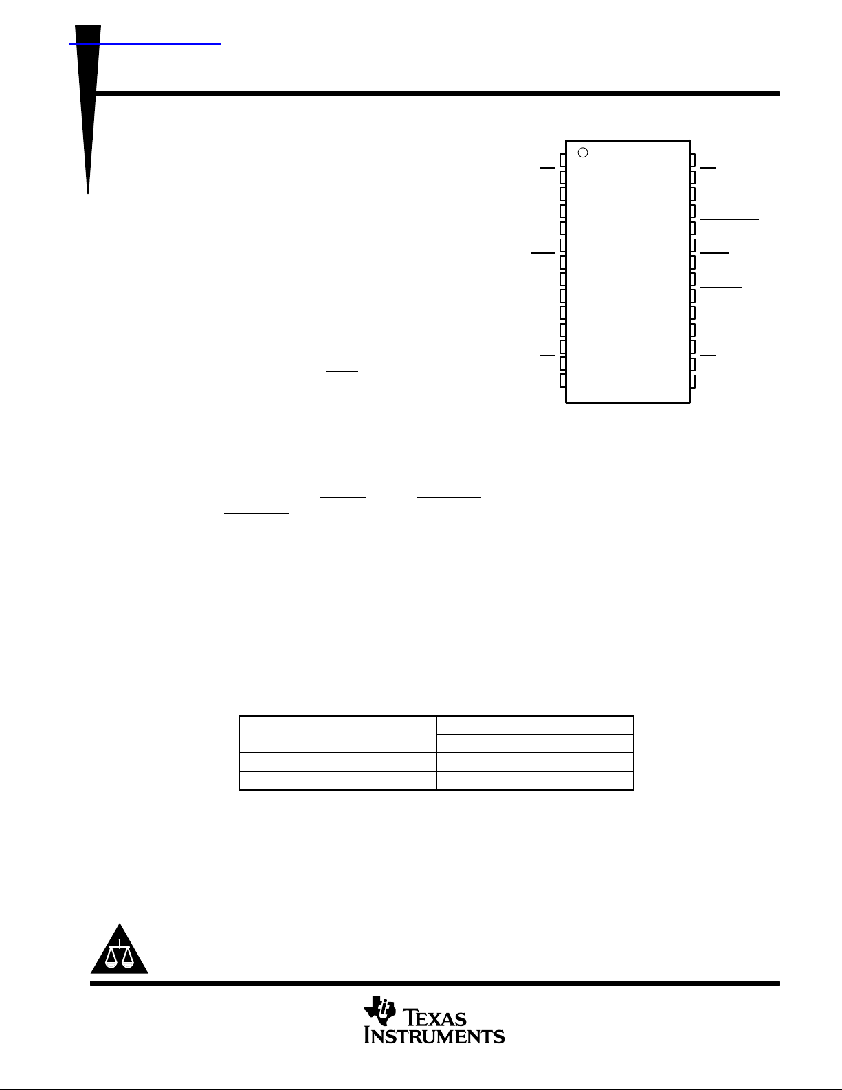
PW PACKAGE
(TOP VIEW)
Applications
D Spread Spectrum Clock Compatible
D Operating Frequency: 60 MHz to 180 MHz
D Low Jitter (cyc–cyc): ±50 ps
D Distributes One Differential Clock Input to
Four Differential Clock Outputs
D Enters Low Power Mode and Three-State
Outputs When Input CLK Signal Is Less
Than 20 MHz or PWRDWN Is Low
D Operates From Dual 2.5-V Supplies
D 28-Pin TSSOP Package
D Consumes < 200-µA Quiescent Current
D External Feedback PIN (FBIN, FBIN) Are
GND
Y0
Y0
V
DDQ
GND
CLK
CLK
V
DDQ
AV
DD
AGND
V
DDQ
Y1
Y1
GND
1
2
3
4
5
6
7
8
9
10
11
12
13
14
28
27
26
25
24
23
22
21
20
19
18
17
16
15
GND
Y3
Y3
V
PWRDWN
FBIN
FBIN
V
FBOUT
FBOUT
V
Y2
Y2
GND
Used to Synchronize the Outputs to the
Input Clocks
description
The CDCV855 is a high-performance, low-skew, low-jitter zero delay buf fer that distributes a dif ferential clock
input pair (CLK, CLK
feedback clock outputs (FBOUT , FBOUT
with CLK. When PWRDWN
shut down (low-power mode). The device also enters this low-power mode when the input frequency falls below
a suggested detection frequency that is below 20 MHz (typical 10 MHz). An input frequency detection circuit
detects the low-frequency condition and after applying a >20-MHz input signal this detection circuit turns on the
PLL again and enables the outputs.
) to four differential pairs of clock outputs (Y[0:3], Y[0:3]) and one differential pair of
). When PWRDWN is high, the outputs switch in phase and frequency
is low, all outputs are disabled to a high-impedance state (3-state), and the PLL is
DDQ
DDQ
DDQ
When A V
is tied to GND, the PLL is turned off and bypassed for test purposes. The CDCV855 is also able
DD
to track spread spectrum clocking for reduced EMI.
Since the CDCV855 is based on PLL circuitry , it requires a stabilization time to achieve phase-lock of the PLL.
This stabilization time is required following power up. The CDCV855 is characterized for both commercial and
industrial temperature ranges.
AVAILABLE OPTIONS
PACKAGED DEVICES
TSSOP (PW)
Copyright 2002, Texas Instruments Incorporated
0°C to 70°C CDCV855PW
–40°C to 85°C CDCV855IPW
Please be aware that an important notice concerning availability, standard warranty, and use in critical applications of
Texas Instruments semiconductor products and disclaimers thereto appears at the end of this data sheet.
PRODUCTION DATA information is current as of publication date.
Products conform to specifications per the terms of Texas Instruments
standard warranty. Production processing does not necessarily include
testing of all parameters.
T
A
POST OFFICE BOX 655303 • DALLAS, TEXAS 75265
1
Page 2
CDCV855, CDCV855I
2.5-V PHASE-LOCK LOOP CLOCK DRIVER
SCAS660A – SEPTEMBER 2001 – REVISED DECEMBER 2002
FUNCTION TABLE
(Select Functions)
INPUTS
AV
DD
GND H L H L H L H Bypassed/Off
GND H H L H L H L Bypassed/Off
X L L H Z Z Z Z Off
X L H L Z Z Z Z Off
2.5 V (nom) H L H L H L H On
2.5 V (nom) H H L H L H L On
2.5 V (nom) X <20 MHz{<20 MHz
†
Typically 10 MHz
functional block diagram
PWRDWN
AV
PWRDWN CLK CLK Y[0:3] Y[0:3] FBOUT FBOUT
24
Powerdown
and Test
Logic
DD
9
OUTPUTS PLL
{
Z Z Z Z Off
3
2
12
13
17
16
26
27
Y0
Y0
Y1
Y1
Y2
Y2
Y3
Y3
23
22
6
7
PLL
CLK
CLK
FBIN
FBIN
Terminal Functions
TERMINAL
NAME NO.
AGND 10 Ground for 2.5-V analog supply
AV
DD
CLK, CLK 6, 7 I Differential clock input
FBIN, FBIN 23, 22 I Feedback differential clock input
FBOUT, FBOUT 19, 20 O Feedback differential clock output
GND 1, 5, 14, 15, 28 Ground
PWRDWN 24 I Control input to turn device in the power-down mode
V
DDQ
Y[0:3] 3, 12, 17, 26 O Buffered output copies of input clock, CLK
Y[0:3] 2, 13, 16, 27 O Buffered output copies of input clock, CLK
4, 8, 11, 18, 21, 25 2.5-V supply
9 2.5-V analog supply
I/O
DESCRIPTION
19
20
FBOUT
FBOUT
2
POST OFFICE BOX 655303 • DALLAS, TEXAS 75265
Page 3
CDCV855, CDCV855I
2.5-V PHASE-LOCK LOOP CLOCK DRIVER
SCAS660A – SEPTEMBER 2001 – REVISED DECEMBER 2002
DDQ
DDQ
†
+ 0.5 V. . . . . . . . . . . . . . . . . . . . . . . . . . . . . . . . . .
+ 0.5 V. . . . . . . . . . . . . . . . . . . . . . . . . . . . . . . .
absolute maximum ratings over operating free-air temperature (unless otherwise noted)
Supply voltage range, V
Input voltage range, V
I
Output voltage range, V
Input clamp current, I
IK
Output clamp current, I
Continuous output current, I
Continuous current to GND or V
Package thermal impedance, θ
Storage temperature range T
†
Stresses beyond those listed under “absolute maximum ratings” may cause permanent damage to the device. These are stress ratings only, and
functional operation of the device at these or any other conditions beyond those indicated under “recommended operating conditions” is not
implied. Exposure to absolute-maximum-rated conditions for extended periods may affect device reliability.
NOTES: 1. The input and output negative voltage ratings may be exceeded if the input and output clamp-current ratings are observed.
2. This value is limited to 3.6 V maximum.
3. The package thermal impedance is calculated in accordance with JESD 51.
AVDD –0.5 V to 3.6 V. . . . . . . . . . . . . . . . . . . . . . . . . . . . . . . . . . . . . . . . . . . . . . . . .
,
DDQ
(see Notes 1 and 2) –0.5 V to V
(see Notes 1 and 2) –0.5 V to V
O
(VI < 0 or V
(VO < 0 or VO > V
OK
O
stg
> V
I
(VO = 0 to V
±100 mA. . . . . . . . . . . . . . . . . . . . . . . . . . . . . . . . . . . . . . . . . . . . . . . . . . . . .
DDQ
(see Note 3): PW package 105.8°C/W. . . . . . . . . . . . . . . . . . . . . . . . . . . . . .
JA
) ±50 mA. . . . . . . . . . . . . . . . . . . . . . . . . . . . . . . . . . . . . . . . . . . . . . .
DDQ
DDQ
) ±50 mA. . . . . . . . . . . . . . . . . . . . . . . . . . . . . . . . . . . . . . . . . .
DDQ
) ±50 mA. . . . . . . . . . . . . . . . . . . . . . . . . . . . . . . . . . . . . . . . . . . .
–65°C to 150°C. . . . . . . . . . . . . . . . . . . . . . . . . . . . . . . . . . . . . . . . . . . . . . . . . . .
recommended operating conditions (see Note 4)
MIN TYP MAX UNIT
Supply voltage, V
Low-level input voltage, V
High-level input voltage, V
DC input signal voltage (see Note 5) –0.3 V
Differential input signal voltage, VID (see Note 6) CLK, FBIN 0.36 V
Output differential cross-voltage, V
Input differential pair cross-voltage, V
High-level output current, I
Low-level output current, I
Input slew rate, SR (see Figure 7) 1 4 V/ns
p
Operating free-air temperature, T
NOTES: 4. Unused inputs must be held high or low to prevent them from floating.
5. DC input signal voltage specifies the allowable dc execution of differential input.
6. Differential input signal voltage specifies the differential voltage |VTR – VCP| required for switching, where VTR is the true input level
and VCP is the complementary input level.
7. Differential cross-point voltage is expected to track variations of V
crossing.
DDQ,
AV
DD
IL
IH
(see Note 7) V
O(X)
(see Note 7) V
I(X)
OH
OL
p
A
CLK, CLK, FBIN, FBIN V
PWRDWN –0.3 0.7
CLK, CLK, FBIN, FBIN V
PWRDWN 1.7 V
Commercial 0 85
Industrial –40 85
and is the voltage at which the differential signals must be
DDQ
2.3 2.7 V
/2 – 0.18
DDQ
/2 + 0.18
DDQ
+ 0.3
DDQ
DDQ
+ 0.6 V
DDQ
/2 – 0.2 V
DDQ
/2 – 0.2 V
DDQ
DDQ
/2 V
/2 + 0.2 V
DDQ
/2 + 0.2 V
DDQ
V
V
V
–12 mA
12 mA
°C
POST OFFICE BOX 655303 • DALLAS, TEXAS 75265
3
Page 4

CDCV855, CDCV855I
2.5-V PHASE-LOCK LOOP CLOCK DRIVER
SCAS660A – SEPTEMBER 2001 – REVISED DECEMBER 2002
electrical characteristics over recommended operating free-air temperature range (unless
otherwise noted)
PARAMETER TEST CONDITIONS MIN TYP
V
IK
V
OH
V
OL
I
OH
I
OL
V
OD
V
OX
I
I
I
OZ
I
DD(PD)
I
DD
AI
DD
C
I
C
O
†
All typical values are at respective nominal V
‡
Differential cross-point voltage is expected to track variation of V
Input voltage All inputs V
High-level output voltage
Low-level output voltage
High-level output current V
Low-level output current V
Output voltage swing
Output differential
cross-voltage
Input current V
High-impedance-state output
current
Power-down current on
V
DDQ
Dynamic current on V
Supply current on AV
Input capacitance V
Output capacitance V
+ AV
}
DD
DDQ
DD
= 2.3 V, II = –18 mA –1.2 V
DDQ
V
= min to max, IOH = –1 mA V
DDQ
V
= 2.3 V,
DDQ
V
= min to max, IOL = 1 mA 0.1
DDQ
V
= 2.3 V,
DDQ
= 2.3 V, VO = 1 V –18 –32 mA
DDQ
= 2.3 V, VO = 1.2 V 26 35 mA
DDQ
Differential outputs are terminated with
120 Ω
= 2.7 V, VI = 0 V to 2.7 V ±10 µA
DDQ
V
= 2.7 V, VO = V
DDQ
CLK and CLK = 0 MHz; PWRDWN = Low;
Σ of IDD and AI
Differential outputs
are terminated with
120 Ω / CL = 14 pF
Differential outputs
are terminated with
120 Ω / CL = 0 pF
fO = 167 MHz 8 10 mA
= 2.5 V VI = V
DDQ
= 2.5 V VO = V
DDQ
DDQ
DD
.
– 0.1
DDQ
IOH = –12 mA 1.7
IOL = 12 mA 0.6
1.1 V
V
/2 – 0.2 V
DDQ
or GND ±10 µA
DDQ
fO = 167 MHz
or GND 2 2.5 3 pF
DDQ
or GND 2.5 3 3.5 pF
DDQ
and is the voltage at which the differential signals must be crossing.
DDQ
†
/2 V
DDQ
100 200 µA
150 180
130 160
DDQ
DDQ
MAX UNIT
– 0.4
/2 + 0.2
V
V
V
mA
timing requirements over recomme nd ed ran ge s of supply voltage and operating free-air
temperature
PARAMETER MIN MAX UNIT
f
CLK
§
Recovery time required when the device goes from power-down mode into bypass mode (test mode with AVDD at GND).
¶
Time required for the integrated PLL circuit to obtain phase lock of its feedback signal to its reference signal. For phase lock to be obtained, a
fixed-frequency , fixed-phase reference signal must be present at CLK. Until phase lock is obtained, the specifications for propagation delay, skew ,
and jitter parameters given in the switching characteristics table are not applicable. This parameter does not apply for input modulation under
SSC application.
Operating clock frequency 60 180 MHz
Input clock duty cycle 40% 60%
Stabilization time (PLL mode)
Stabilization time (Bypass mode)
W
w
10 µs
30 ns
4
POST OFFICE BOX 655303 • DALLAS, TEXAS 75265
Page 5

CDCV855, CDCV855I
§
§
jit(
)
t
jit(h er)
Half eriod jitter, See Figure 6
s
SSC off
w
Dynamic hase offset (this includes jitter)
SSC on
2.5-V PHASE-LOCK LOOP CLOCK DRIVER
SCAS660A – SEPTEMBER 2001 – REVISED DECEMBER 2002
switching characteristics
PARAMETER TEST CONDITIONS MIN TYP†MAX UNIT
}
t
PLH
t
PHL
t
jit(per)
t
jit(cc)
t
hper
t
slr(o)
t
d(Ø)
t
(Ø)
tsk
(o)
tr, tf Output rise and fall times (20% – 80%) Load: 120 Ω/14 pF 650 900 ps
†
All typical values are at a respective nominal V
‡
Refers to transition of noninverting output
§
This parameter is assured by design but can not be 100% production tested.
¶
All differential output pins are terminated with 120 Ω/14 pF.
Low-to-high level propagation delay time Test mode/CLK to any output 4.5 ns
}
High-to-low level propagation delay time Test mode/CLK to any output 4.5 ns
Jitter (period), See Figure 5
Jitter (cycle-to-cycle), See Figure 2
§
Half-period jitter, See Figure 6
Output clock slew rate, See Figure 7
Dynamic phase offset (this includes jitter),
See Figure 3(b)
Static phase offset, See Figure 3(a)
¶
Output skew, See Figure 4 50 ps
DDQ
,
.
66 MHz –55 55 ps
100/133/167/180 MHz
66 MHz –60 60
100/133/167/180 MHz
66 MHz –130 130
100 MHz
133/167/180 MHz –75 75
Load = 120Ω / 14 pF 1 2 V/ns
Load = 120Ω / 4 pF
66 MHz –180 180
SSC off
SSC on
66 MHz –150 150
100/133/167/180 MHz
100/133 MHz –130 130
167/180 MHz –90 90
66 MHz –230 230
100/133 MHz –170 170
167/180 MHz –100 100
–35 35 ps
–50 50
–90 90
1 3 V/ns
–100 100
ps
ps
ps
ps
POST OFFICE BOX 655303 • DALLAS, TEXAS 75265
5
Page 6

CDCV855, CDCV855I
2.5-V PHASE-LOCK LOOP CLOCK DRIVER
SCAS660A – SEPTEMBER 2001 – REVISED DECEMBER 2002
PARAMETER MEASUREMENT INFORMATION
VDD/2
Yx, FBOUT
Yx, FBOUT
CDCV855
–VDD/2
NOTE: V
(TT)
C = 14 pF
Z = 60 Ω
Z = 60 Ω
C = 14 pF
–VDD/2
= GND
–VDD/2
R = 10 Ω
R = 10 Ω
Figure 1. Output Load Test Circuit
t
c(n)
Z = 50 Ω
Z = 50 Ω
t
c(n+1)
SCOPE
V
(TT)
V
(TT)
R = 50 Ω
R = 50 Ω
t
= t
jit(cc)
c(n)
– t
c(n+1)
Figure 2. Cycle-to-Cycle Jitter
6
POST OFFICE BOX 655303 • DALLAS, TEXAS 75265
Page 7

CLK
CLK
FBIN
FBIN
CDCV855, CDCV855I
2.5-V PHASE-LOCK LOOP CLOCK DRIVER
SCAS660A – SEPTEMBER 2001 – REVISED DECEMBER 2002
PARAMETER MEASUREMENT INFORMATION
CLK
CLK
FBIN
FBIN
t
d(φ)
Yx
t
(φ) n
t
=
(φ)
(N is a Large Number of Samples)
(a) Static Phase Offset
t
(φ)
t
d(φ)
(b) Dynamic Phase Offset
∑
n = N
1
N
Figure 3. Phase Offset
t
(φ) n
t
d(φ)
t
(φ) n+1
t
(φ)
t
d(φ)
Yx
Yx, FBOUT
Yx, FBOUT
t
sk(o)
Figure 4. Output Skew
POST OFFICE BOX 655303 • DALLAS, TEXAS 75265
7
Page 8

CDCV855, CDCV855I
2.5-V PHASE-LOCK LOOP CLOCK DRIVER
SCAS660A – SEPTEMBER 2001 – REVISED DECEMBER 2002
PARAMETER MEASUREMENT INFORMATION
Yx, FBOUT
Yx, FBOUT
, FBOUT
Yx
Yx, FBOUT
Figure 5. Period Jitter
Yx
, FBOUT
t
jit(per)
= t
t
c(n)
1
f
o
c(n)
1
–
f
o
Yx, FBOUT
Clock Inputs
and Outputs
t
(hper_n)
1
f
o
t
jit(hper)
= t
(hper_n) –
Figure 6. Half-Period Jitter
80%
20%
t
slrr(i)
, t
slrr(o)
t
slrf(i)
Figure 7. Input and Output Slew Rates
t
(hper_n+1)
2xf
, t
slrf(o)
1
o
80%
20%
VID, V
OD
8
POST OFFICE BOX 655303 • DALLAS, TEXAS 75265
Page 9

CDCV855, CDCV855I
2.5-V PHASE-LOCK LOOP CLOCK DRIVER
SCAS660A – SEPTEMBER 2001 – REVISED DECEMBER 2002
MECHANICAL DATA
PW (R-PDSO-G**) PLASTIC SMALL-OUTLINE PACKAGE
14 PINS SHOWN
0,65
1,20 MAX
14
0,30
0,19
8
4,50
4,30
PINS **
7
Seating Plane
0,15
0,05
8
1
A
DIM
14
0,10
6,60
6,20
M
0,10
0,15 NOM
0°–ā8°
2016
Gage Plane
24
0,25
0,75
0,50
28
A MAX
A MIN
NOTES: A. All linear dimensions are in millimeters.
B. This drawing is subject to change without notice.
C. Body dimensions do not include mold flash or protrusion not to exceed 0,15.
D. Falls within JEDEC MO-153
3,10
2,90
5,10
4,90
5,10
4,90
6,60
6,40
7,90
7,70
9,80
9,60
4040064/F 01/97
POST OFFICE BOX 655303 • DALLAS, TEXAS 75265
9
Page 10

IMPORTANT NOTICE
Texas Instruments Incorporated and its subsidiaries (TI) reserve the right to make corrections, modifications,
enhancements, improvements, and other changes to its products and services at any time and to discontinue
any product or service without notice. Customers should obtain the latest relevant information before placing
orders and should verify that such information is current and complete. All products are sold subject to TI’s terms
and conditions of sale supplied at the time of order acknowledgment.
TI warrants performance of its hardware products to the specifications applicable at the time of sale in
accordance with TI’s standard warranty . Testing and other quality control techniques are used to the extent TI
deems necessary to support this warranty . Except where mandated by government requirements, testing of all
parameters of each product is not necessarily performed.
TI assumes no liability for applications assistance or customer product design. Customers are responsible for
their products and applications using TI components. T o minimize the risks associated with customer products
and applications, customers should provide adequate design and operating safeguards.
TI does not warrant or represent that any license, either express or implied, is granted under any TI patent right,
copyright, mask work right, or other TI intellectual property right relating to any combination, machine, or process
in which TI products or services are used. Information published by TI regarding third–party products or services
does not constitute a license from TI to use such products or services or a warranty or endorsement thereof.
Use of such information may require a license from a third party under the patents or other intellectual property
of the third party , or a license from TI under the patents or other intellectual property of TI.
Reproduction of information in TI data books or data sheets is permissible only if reproduction is without
alteration and is accompanied by all associated warranties, conditions, limitations, and notices. Reproduction
of this information with alteration is an unfair and deceptive business practice. TI is not responsible or liable for
such altered documentation.
Resale of TI products or services with statements different from or beyond the parameters stated by TI for that
product or service voids all express and any implied warranties for the associated TI product or service and
is an unfair and deceptive business practice. TI is not responsible or liable for any such statements.
Mailing Address:
Texas Instruments
Post Office Box 655303
Dallas, Texas 75265
Copyright 2002, Texas Instruments Incorporated
 Loading...