

Page 1
查询CDCV304供应商
CDCV304
140-MHz PCI-X CLOCK BUFFER
SCAS643B – SEPTEMBER 2000 REVISED JUL Y 2002
D
General-Purpose and PCI-X 1:4 Clock
Buffer
D
Operating Frequency: 0 MHz to 140 MHz
D
Low Output Skew: <100 ps
D
Distributes One Clock Input to One Bank of
Four Outputs
D
Output Enable Control That Drives Outputs
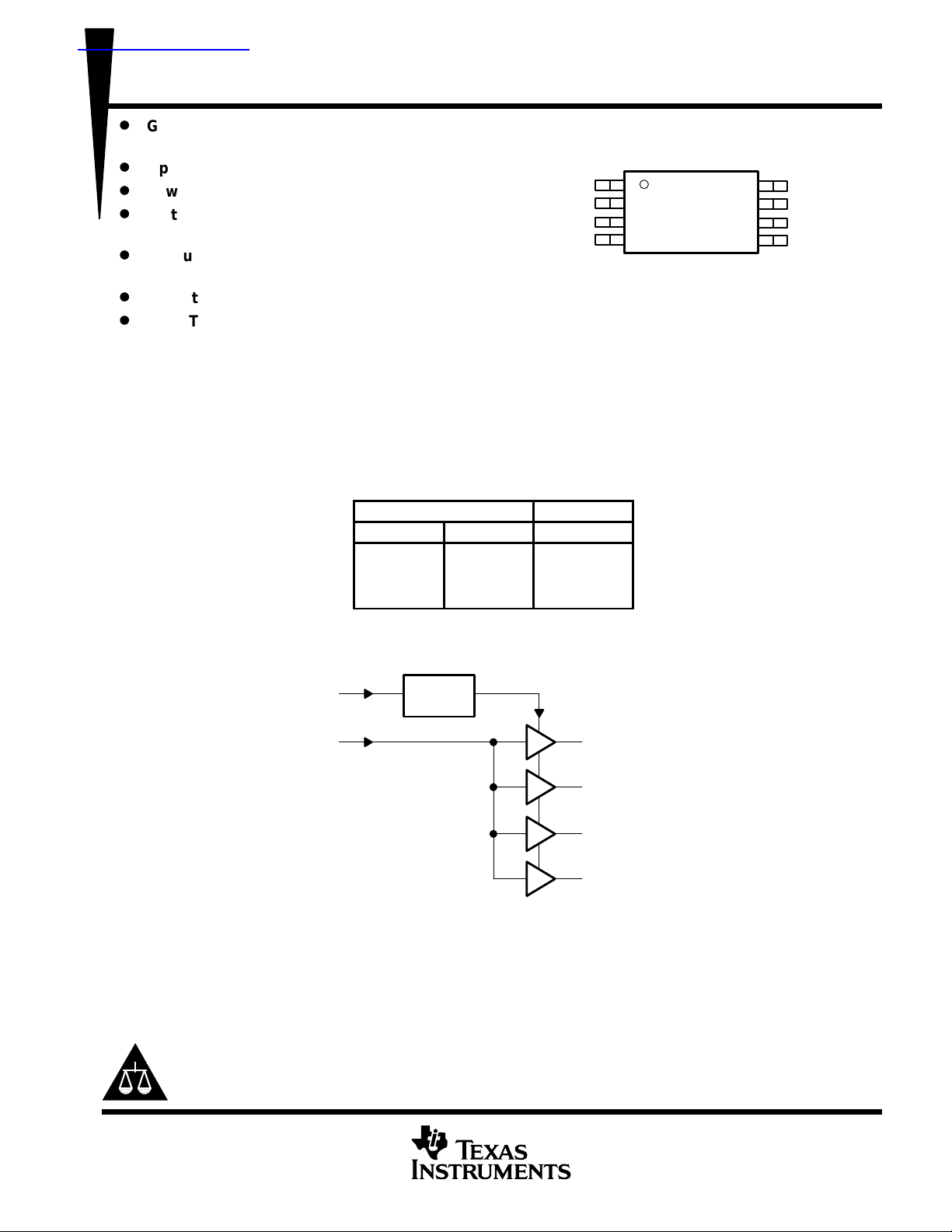
CLKIN
OE
1Y0
GND
TSSOP
PW PACKAGE
(TOP VIEW)
1
2
3
4
8
7
6
5
Low When OE Is Low
D
Operates From Single 3.3-V Supply
D
8-Pin TSSOP Package
description
The CDCV304 is a high-performance, low-skew, general-purpose and PCI-X clock buf fer. It distributes one input
clock signal (CLKIN) to the output clocks (1Y[0:3]). It is specifically designed for use with PCI-X applications.
The CDCV304 operates at 3.3 V.
The CDCV304 is characterized for operation from –40°C to 85°C for automotive and industrial applications.
FUNCTION TABLE
INPUTS
CLKIN OE 1Y (0:3)
L
H
L
H
L
L
H
H
OUTPUT
L
L
L
H
1Y3
1Y2
V
DD
1Y1
3.3V
functional block diagram
Please be aware that an important notice concerning availability, standard warranty, and use in critical applications of
Texas Instruments semiconductor products and disclaimers thereto appears at the end of this data sheet.
OE
CLKIN
2
1
Logic
Control
3
1Y0
5
1Y1
7
1Y2
8
1Y3
PRODUCTION DATA information is current as of publication date.
Products conform to specifications per the terms of Texas Instruments
standard warranty. Production processing does not necessarily include
testing of all parameters.
POST OFFICE BOX 655303 • DALLAS, TEXAS 75265
Copyright 2002, Texas Instruments Incorporated
1
Page 2
CDCV304
I/O
DESCRIPTION
140-MHz PCI-X CLOCK BUFFER
SCAS643B – SEPTEMBER 2000 REVISED JULY 2002
Terminal Functions
TERMINAL
NAME NO.
1Y[0–3] 3, 5, 7, 8 O Buffered output clocks
CLKIN 1 I Input reference frequency
GND 4 Power Ground
OE 2 I Outputs enable control
VDD3.3V 6 Power 3.3-V supply
absolute maximum ratings over operating free-air temperature (unless otherwise noted)
Supply voltage range, V
Input voltage range, V
Output voltage range, V
Input clamp current, I
Output clamp current, I
Continuous total output current, I
Package thermal impedance, θ
Storage temperature range, T
†
Stresses beyond those listed under “absolute maximum ratings” may cause permanent damage to the device. These are stress ratings only, and
functional operation of the device at these or any other conditions beyond those indicated under “recommended operating conditions” is not
implied. Exposure to absolute-maximum-rated conditions for extended periods may affect device reliability.
NOTES: 1. The input and output negative-voltage ratings may be exceeded if the input and output clamp-current ratings are observed.
2. This value is limited to 4.6 V maximum.
3. The package thermal impedance is calculated in accordance with JESD 51.
–0.5 V to 4.3 V. . . . . . . . . . . . . . . . . . . . . . . . . . . . . . . . . . . . . . . . . . . . . . . . . . . . . . . . .
DD
(see Notes 1 and 2) –0.5 V to VDD + 0.5 V. . . . . . . . . . . . . . . . . . . . . . . . . . . . . . . . . . . .
I
(see Notes 1 and 2) –0.5 V to VDD + 0.5 V. . . . . . . . . . . . . . . . . . . . . . . . . . . . . . . . . .
O
(VI < 0 or VI > VDD) ±50 mA. . . . . . . . . . . . . . . . . . . . . . . . . . . . . . . . . . . . . . . . . . . . . . . .
IK
(VO < 0 or VO > VDD) ±50 mA. . . . . . . . . . . . . . . . . . . . . . . . . . . . . . . . . . . . . . . . . . . .
OK
(VO = 0 to VDD) ±50 mA. . . . . . . . . . . . . . . . . . . . . . . . . . . . . . . . . . . . . . . . .
O
(see Note 3): PW package 230.5°C/W. . . . . . . . . . . . . . . . . . . . . . . . . . . . .
JA
–65°C to 150°C. . . . . . . . . . . . . . . . . . . . . . . . . . . . . . . . . . . . . . . . . . . . . . . . . . .
stg
†
recommended operating conditions
MIN NOM MAX UNIT
Supply voltage, V
High-level input voltage, V
Low-level input voltage, V
Input voltage, V
High-level output current, I
Low-level output current, I
Operating free-air temperature, T
DD
IH
IL
I
OH
OL
A
3 3.3 3.6 V
0.7×V
DD
0.3×V
0 V
–40 85 °C
V
DD
DD
–24 mA
V
V
24 mA
timing requirements over recommended ranges of supply voltage and operating free-air
temperature
MIN NOM MAX UNIT
f
clk
2
Clock frequency 0 140 MHz
POST OFFICE BOX 655303 • DALLAS, TEXAS 75265
Page 3
IOHHigh-level output current
mA
IOLLow-level output current
mA
See Figures 1 and 2
T
CLK high time, See Figure 4
ns
T
CLK low time, See Figure 4
ns
CDCV304
140-MHz PCI-X CLOCK BUFFER
SCAS643B – SEPTEMBER 2000 REVISED JULY 2002
electrical characteristics over recommended operating free-air temperature range (unless
otherwise noted)
PARAMETER TEST CONDITIONS MIN TYP†MAX UNIT
V
IK
V
OH
V
OL
I
I
I
DD
C
i
C
o
†
All typical values are at respective nominal VDD and 25°C.
Input voltage VDD = 3 V, II = –18 mA –1.2 V
VDD = min to max, IOH = –1 mA VDD–0.2
High-level output voltage
Low-level output voltage
p
p
Input current VI = VO or V
Dynamic current, See Figure 5 f = 67 MHz 37 mA
Input capacitance VDD = 3.3 V, VI = 0 V or V
Output capacitance VDD = 3.3 V, VI = 0 V or V
VDD = 3 V, IOH = –24 mA
VDD = 3 V, IOH = –12 mA 2.4
VDD = min to max, IOL = 1 mA 0.2
VDD = 3 V, IOL = 24 mA
VDD = 3 V, IOL = 12 mA 0.55
VDD = 3 V, VO = 1 V –50
VDD = 3.3 V, VO = 1.65 V –55
VDD = 3 V, VO = 2 V 60
VDD = 3.3 V, VO = 1.65 V 70
DD
DD
DD
2
0.8
±5 µA
3 pF
3.2 pF
V
V
switching characteristics over recommended ranges of supply voltage and operating free-air
temperature, CL = 10 pF, VDD = 3.3 V ± 0.3 V (see Note 6 and Figures 1 and 2)
PARAMETER TEST CONDITIONS MIN
t
PLH
t
PHL
t
sk(o)
t
sk(p)
t
sk(pr)
t
sk(pp)
high
low
t
r
t
f
†
All typical values are at respective nominal VDD.
‡
This symbol is according to PCI-X terminology.
NOTE 4: The t
High-to-low propagation delay
Low-to-high propagation delay
Output skew (see Note 4) 50 100 ps
Pulse skew VIH = VDD, VIL = 0 V 150 ps
Process skew 0.2 0.3 ns
Part-to-part skew 0.25 0.4 ns
Output rise slew rate
Output fall slew rate
specification is only valid for equal loading of all outputs.
sk(o)
‡
‡
1.8 2.5 3 ns
1.8 2.4 3 ns
66 MHz 6
140 MHz 3
66 MHz 6
140 MHz 3
0.2VDD to 0.6V
0.6VDD to 0.2V
DD
DD
1.5 2.7 4 V/ns
1.5 2.7 4 V/ns
TYP
†
MAX UNIT
POST OFFICE BOX 655303 • DALLAS, TEXAS 75265
3
Page 4

CDCV304
140-MHz PCI-X CLOCK BUFFER
SCAS643B – SEPTEMBER 2000 REVISED JULY 2002
PARAMETER MEASUREMENT INFORMATION
V
DD
140 Ω
Y
n
Any Y
10 pF
140 Ω
Figure 1. Test Load Circuit
V
DD
50% V
DD
CLKIN
1Y0 – 1Y3
t
50% V
0.2 V
PLH
0.6 V
DD
DD
DD
t
PHL
0.6 V
t
r
t
f
DD
50% V
0.2 V
0 V
DD
DD
V
OH
V
OL
Figure 2. Voltage Thresholds for Propagation Delay (tpd) Measurements
50% V
DD
50% V
DD
Any Y
t
sk(0)
Figure 3. Output Skew
PARAMETER VALUE UNIT
V
IH(Min)
V
IL(Max)
V
test
NOTE: All parameters in Figure 4 are according to PCI-X 1.0 specifications.
0.5 V
0.35 V
0.4 V
DD
DD
DD
V
V
V
V
IL(Max)
V
IH(Min)
V
test
Figure 4. Clock Waveform
4
POST OFFICE BOX 655303 • DALLAS, TEXAS 75265
t
high
0.6 V
DD
t
cyc
t
low
0.2 V
DD
Peak to Peak (Minimum)
0.4 V
DD
Page 5

CDCV304
140-MHz PCI-X CLOCK BUFFER
SCAS643B – SEPTEMBER 2000 REVISED JULY 2002
PARAMETER MEASUREMENT INFORMATION
SUPPLY CURRENT
vs
FREQUENCY
60
VDD = 3.6 V
TA = 85°C
50
40
– Supply Current – mA
CC
30
I
20
0 20 40 60 80 100 120 140 160
f – Frequency – MHz
Figure 5
HIGH-LEVEL OUTPUT VOLTAGE
vs
HIGH-LEVEL OUTPUT CURRENT
3.5
VDD = 3.3 V
TA = 25°C
3.0
2.5
2.0
1.5
1.0
– High-Level Output Voltage – V
OH
V
0.5
0
–100 –90 –80 –70 –60 –50 –40 –30 –20 –10 0
IOH – High-Level Output Current – mA
Figure 6
POST OFFICE BOX 655303 • DALLAS, TEXAS 75265
5
Page 6

CDCV304
140-MHz PCI-X CLOCK BUFFER
SCAS643B – SEPTEMBER 2000 REVISED JULY 2002
PARAMETER MEASUREMENT INFORMATION
3.5
VDD = 3.3 V
TA = 25°C
3.0
2.5
2.0
1.5
1.0
OL
V – Low-Level Output Voltage – V
0.5
LOW-LEVEL OUTPUT VOLTAGE
vs
LOW-LEVEL OUTPUT CURRENT
0
–20 0 20 40 60 80 100 120
IOL – Low-Level Output Current – mA
Figure 7
6
POST OFFICE BOX 655303 • DALLAS, TEXAS 75265
Page 7

CDCV304
140-MHz PCI-X CLOCK BUFFER
SCAS643B – SEPTEMBER 2000 REVISED JULY 2002
MECHANICAL DATA
PW (R-PDSO-G**) PLASTIC SMALL-OUTLINE PACKAGE
14 PINS SHOWN
0,65
1,20 MAX
14
0,30
0,19
8
4,50
4,30
PINS **
7
Seating Plane
0,15
0,05
8
1
A
DIM
14
0,10
6,60
6,20
M
0,10
0,15 NOM
0°–8°
2016
Gage Plane
24
0,25
0,75
0,50
28
A MAX
A MIN
NOTES: A. All linear dimensions are in millimeters.
B. This drawing is subject to change without notice.
C. Body dimensions do not include mold flash or protrusion not to exceed 0,15.
D. Falls within JEDEC MO-153
3,10
2,90
5,10
4,90
5,10
4,90
6,60
6,40
7,90
7,70
9,80
9,60
4040064/F 01/97
POST OFFICE BOX 655303 • DALLAS, TEXAS 75265
7
Page 8

IMPORTANT NOTICE
Texas Instruments Incorporated and its subsidiaries (TI) reserve the right to make corrections, modifications,
enhancements, improvements, and other changes to its products and services at any time and to discontinue
any product or service without notice. Customers should obtain the latest relevant information before placing
orders and should verify that such information is current and complete. All products are sold subject to TI’s terms
and conditions of sale supplied at the time of order acknowledgment.
TI warrants performance of its hardware products to the specifications applicable at the time of sale in
accordance with TI’s standard warranty . Testing and other quality control techniques are used to the extent TI
deems necessary to support this warranty . Except where mandated by government requirements, testing of all
parameters of each product is not necessarily performed.
TI assumes no liability for applications assistance or customer product design. Customers are responsible for
their products and applications using TI components. T o minimize the risks associated with customer products
and applications, customers should provide adequate design and operating safeguards.
TI does not warrant or represent that any license, either express or implied, is granted under any TI patent right,
copyright, mask work right, or other TI intellectual property right relating to any combination, machine, or process
in which TI products or services are used. Information published by TI regarding third–party products or services
does not constitute a license from TI to use such products or services or a warranty or endorsement thereof.
Use of such information may require a license from a third party under the patents or other intellectual property
of the third party , or a license from TI under the patents or other intellectual property of TI.
Reproduction of information in TI data books or data sheets is permissible only if reproduction is without
alteration and is accompanied by all associated warranties, conditions, limitations, and notices. Reproduction
of this information with alteration is an unfair and deceptive business practice. TI is not responsible or liable for
such altered documentation.
Resale of TI products or services with statements different from or beyond the parameters stated by TI for that
product or service voids all express and any implied warranties for the associated TI product or service and
is an unfair and deceptive business practice. TI is not responsible or liable for any such statements.
Mailing Address:
Texas Instruments
Post Office Box 655303
Dallas, Texas 75265
Copyright 2002, Texas Instruments Incorporated
 Loading...