

CDCM7005
VCXO LF
VCXO
IN
VCXO
IN
CP
OUT
PRI
REF
YnA
YnB
OSC
DAC
Product
Folder
Order
Now
Technical
Documents
Tools &
Software
Support &
Community
Reference
Design
CDCM7005
SCAS793G –JUNE 2005–REVISED AUGUST 2017
CDCM7005 3.3-V High Performance Clock Synchronizer and Jitter Cleaner
1 Features
1
• High Performance LVPECL and LVCMOS PLL
Clock Synchronizer
• Two Reference Clock Inputs (Primary and
Secondary Clock) for Redundancy Support With
Manual or Automatic Selection
• Accepts LVCMOS Input Frequencies up to 200
MHz
• VCXO_IN Clock is Synchronized to One of the
Two Reference Clocks
• VCXO_IN Frequencies Up to 2.2 GHz (LVPECL)
• Outputs Can Be a Combination of LVPECL and
LVCMOS (Up to Five Differential LVPECL Outputs
or up to 10 LVCMOS Outputs)
• Output Frequency is Selectable by ×1, /2, /3, /4,
/6, /8, /16 on Each Output Individually
• Efficient Jitter Cleaning From Low PLL Loop
Bandwidth
• Low Phase Noise PLL Core
• Programmable Phase Offset (PRI_REF and
SEC_REF to Outputs)
• Wide Charge Pump Current Range From
200 μA to 3 mA
• Dedicated Charge Pump Supply (VCC_CP) for
Wide Tuning Voltage Range VCOs
• Presets Charge Pump to VCC_CP/2 for Fast
Center-Frequency Setting of VC(X)O
• Analog and Digital PLL Lock Indication
• Provides VBB Bias Voltage Output for SingleEnded Input Signals (VCXO_IN)
• Frequency Hold-Over Mode Improves Fail-Safe
Operation
• Power-up Control Forces LVPECL Outputs to 3State at VCC< 1.5 V
• SPI Controllable Device Setting
• 3.3-V Power Supply
• Packaged in 64-Pin BGA (0.8 mm Pitch – ZVA) or
48-Pin QFN (RGZ)
• Industrial Temperature Range –40°C to 85°C
3 Description
The CDCM7005 is a high-performance, low phase
noise and low skew clock synchronizer that
synchronizes a VCXO (voltage controlled crystal
oscillator) or VCO (voltage controlled oscillator)
frequency to one of the two reference clocks. The
programmable pre-divider M and the feedbackdividers N and P give a high flexibility to the
frequency ratio of the reference clock to VC(X)O
VC(X)O_IN clock operates up to 2.2 GHz. Through
the selection of external VC(X)O and loop filter
components, the PLL loop bandwidth and damping
factor can be adjust to meet different system
requirements.
The CDCM7005 can lock to one of two reference
clock inputs (PRI_REF and SEC_REF), supports
frequency hold-over mode and fast-frequency-locking
for fail-safe and increased system redundancy. The
outputs of the CDCM7005 are user definable and can
be any combination of up to five LVPECL outputs or
up to 10 LVCMOS outputs. The built in
synchronization latches ensure that all outputs are
synchronized for low output skew.
Device Information
PART NUMBER PACKAGE BODY SIZE (NOM)
CDCM7005
(1) For all available packages, see the orderable addendum at
the end of the data sheet.
VQFN (48) 7.00 mm × 7.00 mm
BGA (64) 8.00 mm × 8.00 mm
Typical Application Schematic
(1)
2 Applications
• Wireless Infrastructure
• SONET
• Data Communication
• Test Equipment
1
An IMPORTANT NOTICE at the end of this data sheet addresses availability, warranty, changes, use in safety-critical applications,
intellectual property matters and other important disclaimers. PRODUCTION DATA.
CDCM7005
SCAS793G –JUNE 2005–REVISED AUGUST 2017
www.ti.com
Table of Contents
1 Features.................................................................. 1
2 Applications ........................................................... 1
3 Description ............................................................. 1
4 Revision History..................................................... 2
5 Description (continued)......................................... 4
6 Pin Configuration and Functions......................... 4
7 Specifications......................................................... 7
7.1 Absolute Maximum Ratings...................................... 7
7.2 ESD Ratings.............................................................. 7
7.3 Recommended Operating Conditions....................... 7
7.4 Thermal Information.................................................. 8
7.5 Electrical Characteristics........................................... 8
7.6 Timing Requirements.............................................. 10
7.7 Typical Characteristics............................................ 11
8 Parameter Measurement Information ................ 12
9 Detailed Description............................................ 15
9.1 Overview................................................................. 15
9.2 Functional Block Diagram....................................... 16
9.3 Feature Description................................................. 16
9.4 Device Functional Modes........................................ 24
9.5 Programming........................................................... 25
10 Application and Implementation........................ 34
10.1 Application Information.......................................... 34
10.2 Typical Application ............................................... 37
11 Power Supply Recommendations ..................... 40
12 Layout................................................................... 40
12.1 Layout Guidelines ................................................. 40
12.2 Layout Example .................................................... 41
13 Device and Documentation Support ................. 43
13.1 Receiving Notification of Documentation Updates 43
13.2 Community Resources.......................................... 43
13.3 Trademarks........................................................... 43
13.4 Electrostatic Discharge Caution............................ 43
13.5 Glossary................................................................ 43
14 Mechanical, Packaging, and Orderable
Information........................................................... 43
4 Revision History
NOTE: Page numbers for previous revisions may differ from page numbers in the current version.
Changes from Revision F (July 2015) to Revision G Page
• Removed duplicate row: PRI_SEC_CLK................................................................................................................................ 5
• Changed text from: "STATUS_REF or" to: "STATUS_REF or PRI_SEC_CLK".................................................................... 6
Changes from Revision E (February 2013) to Revision F Page
• Added Pin Configuration and Functions section, ESD Ratings table, Feature Description section, Device Functional
Modes, Application and Implementation section, Power Supply Recommendations section, Layout section, Device
and Documentation Support section, and Mechanical, Packaging, and Orderable Information section .............................. 1
Changes from Revision D (August 2009) to Revision E Page
• Changed PLL_LOCK pin description, replaced cycle-slip text............................................................................................... 5
• Changed the Frequency Hold-Over Mode section............................................................................................................... 22
• Changed text From: Cycle-Slip To: Frequency Offset in Figure 21 ..................................................................................... 23
• Changed Note 1 of table Word 3.......................................................................................................................................... 29
• Changed table Word 3, Cycle Slip (Bit 6) To: Frequency Offset.......................................................................................... 29
• Changed table Lock-Detect Window (Word 3) - Clip slip To: Frequency offset, and Note 2............................................... 32
Changes from Revision C (December 2007) to Revision D Page
• Added text to the CTRL_CLK pin - Unused or floating inputs must be tied to proper logic level. A 20kΩ or larger
pull−up resistor to VCC is recommended. ............................................................................................................................. 4
• Added text to the CTRL_DATA pin - Unused or floating inputs must be tied to proper logic level. A 20kΩ or larger
pull−up resistor to VCC is recommended. ............................................................................................................................. 4
• Added text to the CTRL_LE pin - Unused or floating inputs must be tied to proper logic level. A 20kΩ or larger
pull−up resistor to VCC is recommended. ............................................................................................................................. 4
• Added text to the PD pin - It is recommended to ramp up the PD with the same time as VCCand AVCCor later. The
2
Submit Documentation Feedback Copyright © 2005–2017, Texas Instruments Incorporated
Product Folder Links: CDCM7005
CDCM7005
www.ti.com
ramp up rate of the PD should not be faster than the ramp up rate of VCCand AVCC........................................................... 5
• Changed VCC pin text From: 3.3-V supply. There is no internal connection between VCCand AVCC. It is
recommended that AVCCuse its own supply filter. To: 3.3-V supply. VCCand AVCCshould always have the same
supply voltage. It is recommended that AVCCuse its own supply filter.................................................................................. 6
• Added text to the SPI CONTROL INTERFACE section - Unused or floating inputs must be tied to proper logic level.
A 20kΩ or larger pull−up resistor to VCC is recommended. ............................................................................................... 25
• Added text to the SPI CONTROL INTERFACE section - It is recommended to program Word 0, Word 1, Word 2
and Word 3 right after power up and PD becomes HIGH.................................................................................................... 25
• Changed From: RES To: GTME........................................................................................................................................... 29
• Changed From: RES To: PFDFC......................................................................................................................................... 29
Changes from Revision B (October 2005) to Revision C Page
• Changed N2, From: 1 To: 0.................................................................................................................................................. 30
• Changed N3, From: 1 To: 0.................................................................................................................................................. 30
• Changed N3, From: 1 To: 0.................................................................................................................................................. 30
• Changed N2, From: 1 To: 0.................................................................................................................................................. 30
Changes from Revision A (June 2005) to Revision B Page
SCAS793G –JUNE 2005–REVISED AUGUST 2017
• Added minor updates. ............................................................................................................................................................ 1
Changes from Original (June 2005) to Revision A Page
• Changed data sheet from Product Preview to Production data. ............................................................................................ 1
Product Folder Links: CDCM7005
Submit Documentation FeedbackCopyright © 2005–2017, Texas Instruments Incorporated
3
P0022-01
CP_OUTREF_SELPRI_REF
GND GND GND GND GND GND GND
SEC_REF
GND AVCC AVCC AVCC AVCC AVCC
STATUS_
REFor
PRI_SEC_
CLK
GND GND GND GND GND VCC
STATUS_
VCXO
VCXO_IN
GND VCC VCC VCC VCC VCC VCC
Y0A GND GND GND GND GND VCC Y4B
Y0B VCC VCC VCC VCC VCCVCC Y4A
PD Y1A Y1B Y2A Y2B Y3A Y3B
RESET
or
HOLD
1 2 3 4 5 6 7 8
A
B
C
D
F
G
H
I_REF_CP
or
PLL_LOCK
VBB
VCC_CP
CTRL_LE CTRL_CLK
CTRL_
DATA
VCXO_IN
E
P0023-01
1 2 3 4 5 6 7 8 9 10 11 12
36 35 34 33 32 31 30 29 28 27 26 25
37
38
39
40
41
45
44
43
42
46
47
48
24
23
22
21
20
16
17
18
19
15
14
13
ThermalPad
mustbe
solderedtoGND
STATUS_REFor
PRI_SEC_CLK
STATUS_VCXOor
I_REF_CP
RESET
HOLD
or
PD
VCC
Y1A
Y1B
VCC
VCC
Y2A
Y2B
VCC
VCC
Y3A
Y3B
PRI_REF
REF_SEL
NC
VCC_CP
AVCC
CP_OUT
AVCC
CTRL_LE
CTRL_CLK
AVCC
CTRL_DATA
PLL_LOCK
GND
VCC
VCC
VCC
VCC
Y4B
Y4A
VCC
VCC
SEC_REF
AVCC
AVCC
VBB
VCC
VCXO_IN
VCC
VCC
Y0A
Y0B
VCC
VCXO_IN
CDCM7005
SCAS793G –JUNE 2005–REVISED AUGUST 2017
www.ti.com
5 Description (continued)
All device settings, like outputs signaling, divider value, and input selection are programmable by SPI (3-wire
serial peripheral interface). SPI allows individually control of the device settings.
The device operates in 3.3-V environment and is characterized for operation from –40°C to 85°C.
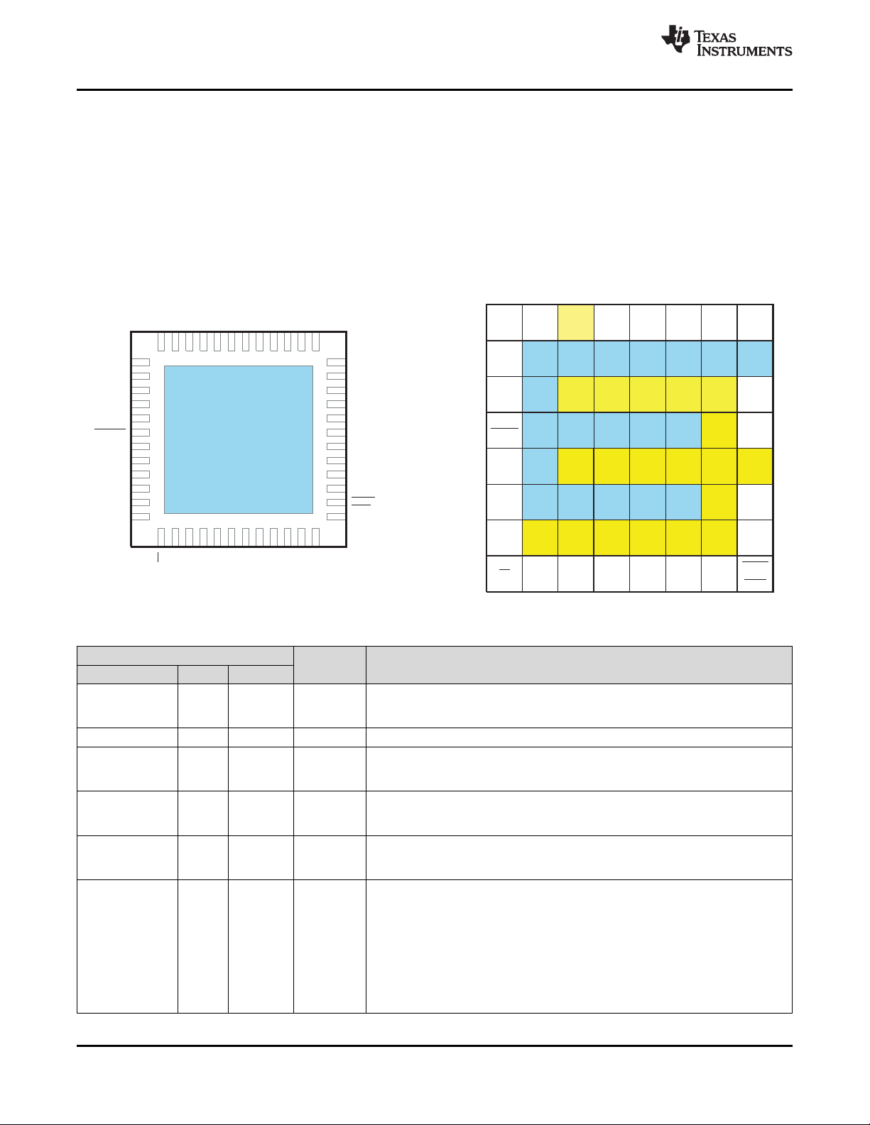
6 Pin Configuration and Functions
RGZ Package
48-Pin VQFN
Top View
PIN
NAME BGA QFN
C3, C4,
AVCC
C5, C6,
C7
CP_OUT A4 31 O Charge pump output
CTRL_CLK A6 28 I
CTRL_DATA A7 26 I
B2, B3,
B4, B5,
B6, B7,
B8, C2,
D2, D3,
D4, D5,
D6, E2,
F2, F3,
F4, F5,
F6
CTRL_LE A5 29 I
GND
4
Submit Documentation Feedback Copyright © 2005–2017, Texas Instruments Incorporated
27, 30,
32, 38,
Thermal
pad and
pin 24
39
Pin Functions
I/O DESCRIPTION
Analog
Power
Ground Ground
3.3-V analog power supply. There is no internal connection between AVCCand
VCC. It is recommended that AVCCuse its own supply filter.
LVCMOS input, serial control clock input for SPI, with hysteresis. Unused or
floating inputs must be tied to proper logic level. A 20kΩ or larger pull−up resistor
to VCC is recommended.
LVCMOS input, serial control data input for SPI, with hysteresis. Unused or
floating inputs must be tied to proper logic level. A 20kΩ or larger pull−up resistor
to VCC is recommended.
LVCMOS input, control latch enable for serial programmable Interface (SPI), with
hysteresis. Unused or floating inputs must be tied to proper logic level. A 20kΩ or
larger pull−up resistor to VCC is recommended.
Product Folder Links: CDCM7005
ZVA Package
64-Pin BGA
Top View
www.ti.com
PIN
NAME BGA QFN
HOLD H8 14 I
I_REF_CP D8 22 O
PD H1 1 I
PLL_LOCK A8 25 I/O
PRI_REF A1 36 I
REF_SEL A2 35 I
SCAS793G –JUNE 2005–REVISED AUGUST 2017
Pin Functions (continued)
I/O DESCRIPTION
This LVCMOS input can be programmed (SPI) to act as HOLD or RESET. RESET
is the default function. This pin is low active and can be activated external or via
the corresponding bit in the SPI register. In case of RESET, the charge pump (CP)
is switched to 3-state and all counters (N, M, P) are reset to zero (the initial divider
settings are maintained in SPI registers). The LVPECL outputs are static low and
high respectively and the LVCMOS outputs are all low or high if inverted. RESET
is not edge triggered and should have a pulse duration of at least 5 ns.
In case of HOLD, the CP is switched in to 3-state mode only. After HOLD is
released and with the next valid reference clock cycle the charge pump is
switched back in to normal operation (CP stays in 3-state as long as no reference
clock is valid). During HOLD, the P divider and all outputs Yx are at normal
operation. This mode allows an external control of the frequency hold-over mode.
The input has an internal 150-kΩ pullup resistor.
This LVCMOS output can be programmed (SPI) to provide either the
STATUS_VCXO information or serve as current path for the charge pump (CP).
STATUS_VCXO is the default setting.
In case of STATUS_VCXO, the LVCMOS output provides the status of the VCXO
input (frequencies above 2 MHz are interpreted as valid clock; active high).
In case of I_REF_CP, it provides the current path for the external reference
resistor (12 kΩ ±1%) to support an accurate charge pump current, optional. Do not
use any capacitor across this resistor to prevent noise coupling via this node. If
the internal 12 kΩ is selected (default setting), this pin can be left open.
LVCMOS input, asynchronous power down (PD) signal. This pin is low active and
can be activated external or by the corresponding bit in the SPI register (in case of
logic high, the SPI setting is valid). Switches the device into power-down mode.
Resets M- and N-Divider, 3-states charge pump, STATUS_REF, or
PRI_SEC_CLK pin, STATUS_VCXO or I_REF_CP pin, PLL_LOCK pin, VBB pin
and all Yx outputs. Sets the SPI register to default value; has internal 150-kΩ
pullup resistor. It is recommended to ramp up the PD with the same time as V
and AVCCor later. The ramp up rate of the PD should not be faster than the ramp
up rate of VCCand AVCC.
LVCMOS output for PLL_LOCK information. This pin is set high if the PLL is in
lock (see feature description). This output can be programmed to be digital lock
detect or analog lock detect (see feature description).
The PLL is locked (set high), if the rising edge either of PRI_REF or SEC_REF
clock and VCXO_IN clock at the phase frequency detector (PFD) are inside the
lock detect window for a predetermined number of successive clock cycles.
The PLL is out-of-lock (set low), if the rising edge of either the PRI_REF or
SEC_REF) clock and VCXO_IN clock at the PFD are outside the lock detect
window or if a certain frequency offset between reference frequency and feedback
frequency (VCXO) is detected.
Both, the lock detect window and the number of successive clock cycles are user
definable (via SPI).
LVCMOS input for the primary reference clock, with an internal 150-kΩ pullup
resistor and input hysteresis.
LVCMOS reference clock selection input. In the manual mode the REF_SEL
signal selects one of the two input clocks:
REF_SEL [1]: PRI_REF is selected;
REF_SEL [0]: SEC_REF is selected;
The input has an internal 150-kΩ pullup resistor.
CDCM7005
CC
Product Folder Links: CDCM7005
Submit Documentation FeedbackCopyright © 2005–2017, Texas Instruments Incorporated
5
CDCM7005
SCAS793G –JUNE 2005–REVISED AUGUST 2017
Pin Functions (continued)
PIN
NAME BGA QFN
RESET H8 14 I
SEC_REF B1 37 I
STATUS_REF or
PRI_SEC_CLK
STATUS_VCXO D8 22 O
VBB C1 40 O
VCC
VCC_CP A3 33 Power
VCXO_IN E1 43 I VCXO LVPECL input
VCXO_IN D1 42 I Complementary VCXO LVPECL input
Y0A:Y0B
Y1A:Y1B
Y2A:Y2B
Y3A:Y3B
Y4A:Y4B
C8 23 O
D7, E3,
E4, E5,
E6, E7,
E8, F7,
G2, G3,
G4, G5,
G6, G7
F1, G1,
H2, H3,
H4, H5,
H6, H7,
G8, F8
2, 5, 6,
9, 10,
13, 15,
18, 19,
20, 21,
41, 44,
45; 48
46, 47,
3, 4,
7, 8,
11,12,
16, 17
I/O DESCRIPTION
This LVCMOS input can be programmed (SPI) to act as HOLD or RESET. RESET
is the default function. This pin is low active and can be activated external or via
the corresponding bit in the SPI register. In case of RESET, the charge pump (CP)
is switched to 3-state and all counters (N, M, P) are reset to zero (the initial divider
settings are maintained in SPI registers). The LVPECL outputs are static low and
high respectively and the LVCMOS outputs are all low or high if inverted. RESET
is not edge triggered and should have a pulse duration of at least 5 ns.
In case of HOLD, the CP is switched in to 3-state mode only. After HOLD is
released and with the next valid reference clock cycle the charge pump is
switched back in to normal operation (CP stays in 3-state as long as no reference
clock is valid). During HOLD, the P divider and all outputs Yx are at normal
operation. This mode allows an external control of the frequency hold-over mode.
The input has an internal 150-kΩ pullup resistor.
LVCMOS input for the secondary reference clock, with an internal 150-kΩ pullup
resistor and input hysteresis.
This output can be programmed (SPI) to provide either the STATUS_REF or
PRI_SEC_CLK information. This pin is set high if one of the STATUS conditions is
valid. STATUS_REF is the default setting.
In case of STATUS_REF, the LVCMOS output provides the Status of the
Reference Clock. If a reference clock with a frequency above 2 MHz is provided to
PRI_REF or SEC_REF STATUS_REF will be set high.
In case of PRI_SEC_CLK, the LVCMOS output indicates whether the primary
clock [high] or the secondary clock [low] is selected.
This LVCMOS output can be programmed (SPI) to provide either the
STATUS_VCXO information or serve as current path for the charge pump (CP).
STATUS_VCXO is the default setting.
In case of STATUS_VCXO, the LVCMOS output provides the status of the VCXO
input (frequencies above 2 MHz are interpreted as valid clock; active high).
In case of I_REF_CP, it provides the current path for the external reference
resistor (12 kΩ ±1%) to support an accurate charge pump current, optional. Do not
use any capacitor across this resistor to prevent noise coupling via this node. If
the internal 12 kΩ is selected (default setting), this pin can be left open.
Bias voltage output to be used to bias unused complementary input VCXO_IN for
single ended signals. The output of VBB is VCC– 1.3 V. The output current is
limited to about 1.5 mA.
Power
O
3.3-V supply. VCCand AVCCshould always have the same supply voltage. It is
recommended that AVCCuse its own supply filter.
This is the charge pump power supply pin used to have the same supply as the
external VCO. It can be set from 2.3 V to 3.6 V.
The outputs of the CDCM7005 are user definable and can be any combination of
up to five LVPECL outputs or up to 10 LVCMOS outputs. The outputs are
selectable via SPI (Word 1, Bit 2-6). The power-up setting is all outputs are
LVPECL.
www.ti.com
6
Submit Documentation Feedback Copyright © 2005–2017, Texas Instruments Incorporated
Product Folder Links: CDCM7005
CDCM7005
www.ti.com
SCAS793G –JUNE 2005–REVISED AUGUST 2017
7 Specifications
7.1 Absolute Maximum Ratings
over operating free-air temperature range (unless otherwise noted)
VCC, A
V
CC_CP
V
I
V
O
I
OUT
I
IN
T
J
T
stg
,
Supply voltage
VCC
Input voltage
Output voltage
Output current for LVPECL/LVCMOS outputs
(0 < VO< VCC)
Input current (VI< 0, VI> VCC) ±20 mA
Maximum junction temperature 125 °C
Storage temperature –65 150 °C
(1) Stresses beyond those listed under Absolute Maximum Ratings may cause permanent damage to the device. These are stress ratings
only, and functional operation of the device at these or any other conditions beyond those indicated under Recommended Operating
Conditions is not implied. Exposure to absolute–maximum–rated conditions for extended periods may affect device reliability.
(2) All supply voltages have to be supplied at the same time.
(3) The input and output negative voltage ratings may be exceeded if the input and output clamp-current ratings are observed.
(2)
(3)
(3)
7.2 ESD Ratings
Human body model (HBM), per ANSI/ESDA/JEDEC JS-001
V
(ESD)
(1) JEDEC document JEP155 states that 500-V HBM allows safe manufacturing with a standard ESD control process.
(2) JEDEC document JEP157 states that 250-V CDM allows safe manufacturing with a standard ESD control process.
Electrostatic discharge
Charged-device model (CDM), per JEDEC specification JESD22-
(2)
C101
(1)
MIN MAX UNIT
–0.5 4.6 V
–0.5 VCC+ 0.5 V
–0.5 VCC+ 0.5 V
±50 mA
VALUE UNIT
(1)
±2500
±1500
V
7.3 Recommended Operating Conditions
MIN NOM MAX UNIT
VCC, AV
CC
V
CC_CP
V
IL
V
IH
I
OH
I
OL
V
I
V
INPP
V
IC
T
A
Supply voltage
Low-level input voltage LVCMOS, see
High-level input voltage LVCMOS, see
(1)
(1)
High-level output current LVCMOS (includes all status pins) –8 mA
Low-level output current LVCMOS (includes all status pins) 8 mA
Input voltage range LVCMOS 0 3.6 V
Input amplitude LVPECL (V
VCXO_IN
– V
VCXO_IN
(2)
)
Common-mode input voltage LVPECL 1 VCC–0.3 V
Operating free-air temperature –40 85 °C
(1) VILand VIHare required to maintain ac specifications; the actual device function tolerates a smaller input level of 1V, if an ac-coupling to
VCC/2 is provided.
(2) V
minimum and maximum is required to maintain ac specifications; the actual device function tolerates at a minimum V
INPP
of 150 mV.
3 3.3 3.6
2.3 V
0.3 V
0.7 V
CC
0.5 1.3 V
CC
CC
INPP
V
V
V
Product Folder Links: CDCM7005
Submit Documentation FeedbackCopyright © 2005–2017, Texas Instruments Incorporated
7
CDCM7005
SCAS793G –JUNE 2005–REVISED AUGUST 2017
www.ti.com
7.4 Thermal Information
CDCM7005
RGZ
(VQFN)
ZVA
(BGA)
48 PINS 64 PINS
UNIT
°C/W
°C/W
THERMAL METRIC
(1)
RGZ
AIRFLOW
(lfm)
ZVA
AIRFLOW
(m/s)
0 0 29.9 53.9
R
θJA
Junction-to-ambient thermal resistance
150 1 24.7 49.8
250 2 23.2 48.5
500 – 21.5 –
R
θJC(top)
R
θJB
Junction-to-case (top) thermal resistance 22.4 28.3 °C/W
Junction-to-board thermal resistance 14.2 38.6 °C/W
0 0 0.2 0.7
ψ
JT
Junction-to-top characterization parameter
150 1 0.2 0.7
250 2 0.2 0.8
500 – 0.3 –
ψ
JB
R
θJC(bot)
Junction-to-board characterization parameter – – °C/W
Junction-to-case (bottom) thermal resistance °C/W
(1) For more information about traditional and new thermal metrics, see the Semiconductor and IC Package Thermal Metrics application
report.
7.5 Electrical Characteristics
over recommended operating free-air temperature range (unless otherwise noted)
PARAMETER TEST CONDITIONS MIN TYP
OVERALL
f
= 245.76 MHz,
VCXO
f
= 30.72 MHz,
I
CC_LVPECL
I
CC_LVCMOS
I
CCPD
I
OZ
V
I_REF_CP
V
BB
C
O
C
I
LVCMOS
f
clk
V
IK
I
I
Supply current (ICCover frequency see
Figure 1 through Figure 4)
Power-down current
High-impedance state output current for Yx
outputs
Voltage on I_REF_CP (external current path
for accurate charge pump current)
Output reference voltage VCC= 3 V – 3.6 V; IBB= –0.2 mA VCC–1.3 V
Output capacitance for Yx VCC= 3.3 V, VO= 0 V or V
Input capacitance at PRI_REF and
SEC_REF
Input capacitance at CTRL_LE,
CTRL_CLOCK, CTRL_DATA
Output frequency, see
Figure 7
LVCMOS input clamp voltage VCC= 3 V, II= –18 mA –1.2 V
LVCMOS input current for CTRL_LE,
CTRL_CLK, CTRL_DATA
(2),(3)
, Figure 6, and
REF_IN
PFD = 240 kHz, ICP= 2 mA, all outputs are LVPECL
and Div-by-8 (load, see Figure 13)
f
= 245.76 MHz,
VCXO
f
= 30.72 MHz,
REF_IN
PFD = 240 kHz, ICP= 2 mA, All outputs are
LVCMOS and Div-by-8 (load, 10 pF)
fIN= 0 MHz, VCC= 3.6 V, AVCC= 3.6 V,
V
= 3.6 V,
CC_CP
VI= 0 V or V
VO= 0 V or VCC– 0.8 V ±40 µA
VO= 0 V or V
12 kΩ to GND at pin D8 (BGA), pin 22 (QFN) 1.21 V
VI= 0 V or VCC, VI= 0 V or V
VI= 0 V or V
Load = 5 pF to GND, 1 kΩ to VCC, 1 kΩ to GND 250 MHz
VI= 0 V or VCC, VCC= 3.6 V ±5 µA
CC
CC
CC
CC
CC
(1)
MAX UNIT
210 260 mA
120 150 mA
100 300 µA
±100 µA
2 pF
2.7
2
pF
(1) All typical values are at VCC= 3.3 V, temperature = 25°C.
(2) f
can be up to 400 MHz in the typical operating mode (25°C / 3.3-V VCC). The total power consumption limit of 700 mW for the BGA
clk
package can be violated if several LVCMOS outputs switch at high frequency (see Figure 3 and Figure 4).
(3) Operating the LVCMOS or LVPECL output above the maximum frequency will not cause a malfunction to the device, but the output
signal swing may no longer meet the output specification.
8
Submit Documentation Feedback Copyright © 2005–2017, Texas Instruments Incorporated
Product Folder Links: CDCM7005
www.ti.com
Electrical Characteristics (continued)
CDCM7005
SCAS793G –JUNE 2005–REVISED AUGUST 2017
over recommended operating free-air temperature range (unless otherwise noted)
PARAMETER TEST CONDITIONS MIN TYP
LVCMOS input current for PD, RESET,
I
IH
HOLD, REF_SEL, PRI_REF, SEC_REF,
(4)
(see
)
VI= VCC, VCC= 3.6 V 5 µA
LVCMOS input current for PD, RESET,
I
IL
V
OH
HOLD, REF_SEL, PRI_REF, SEC_REF,
(4)
(see
)
High-level output voltage for LVCMOS
outputs
VI= 0 V, VCC= 3.6 V –15 –35 µA
VCC= min to max,
IOH= –100 μA
VCC–0.1
VCC= 3 V, IOH= –6 mA 2.4
VCC= 3 V, IOH= –12 mA 2
VCC= min to max,
V
OL
Low-level output voltage for LVCMOS
outputs
IOL= 100 μA
VCC= 3 V, IOL= 6 mA 0.5
VCC= 3 V, IOL= 12 mA 0.8
I
OH
I
OL
tpho Phase offset (REF_IN to Y output)
t
sk(p)
t
pd(LH)
t
pd(HL)
t
sk(o)
High-level output current VCC= 3.3 V, VO= 1.65 V –30 mA
Low-level output current VCC= 3.3 V, VO= 1.65 V 33 mA
(5)
VREF_IN = VCC/2, Y = VCC/2,
see Figure 11, Load = 10 pF
LVCMOS pulse skew, see Figure 10 Crosspoint to VCC/2 load, see Figure 12 150 ps
Propagation delay from VCXO_IN to Yx,
see Figure 10
LVCMOS single-ended output skew, see
and Figure 10
Crosspoint to VCC/2,
Load = 10 pF, see Figure 12 (PLL bypass mode)
(6)
All outputs have the same divider ratio 55
2 2.5 3 ns
Outputs have different divider ratios 70
Duty cycle LVCMOS VCC/2 to VCC/2 49% 51%
t
slew-rate
Output rise/fall slew rate
20% to 80% of swing (load
see Figure 12)
2.4 3.5 V/ns
LVPECL
f
clk
I
I
V
OH
V
OL
Output frequency, see
LVPECL input current VI= 0 V or V
LVPECL high-level output voltage Load, See Figure 13 VCC–1.18
LVPECL low-level output voltage Load, See Figure 13 VCC–2
(3)
and Figure 5 Load, see Figure 13 0 1500 MHz
CC
|VOD| Differential output voltage See Figure 9 and load, see Figure 13 500 mV
t
pho
t
pd(LH)
t
pd(HL)
t
sk(p)
Phase offset (REF_IN to Y output)
Propagation delay time, VCXO_IN to Yx,
see Figure 10
LVPECL pulse skew, see Figure 10
(6)
VREF_IN = VCC/2 to cross point of Y, see Figure 11 –200 100 ps
Cross point-to-cross point, load
see Figure 13
340 490 640 ps
Cross point-to-cross point, load
see Figure 13
Load see Figure 13, all outputs have the same
t
sk(o)
LVPECL output skew
(6)
divider ratio
Load see Figure 13, outputs have
different divider ratios
tr/ t
C
f
I
Rise and fall time 20% to 80% of V
, see Figure 9 120 170 220 ps
OUTPP
Input capacitance at VCXO_IN, VCXO_IN 1.5 pF
LVCMOS-TO-LVPECL
t
sk(P_C)
Output skew between LVCMOS and
LVPECL outputs, see
(7)
and Figure 10
Cross point to VCC/2; load,
see Figure 12 and Figure 13
1.7 2 2.4 ns
PLL ANALOG LOCK
I
OH
I
OL
High-level output current VCC= 3.6 V, VO= 1.8 V –110 µA
Low-level output current VCC= 3.6 V, VO= 1.8 V 110 µA
(4) These inputs have an internal 150-kΩ pullup resistor.
(5) This is valid only for the same frequency of REF_IN clock and Y output clock. It can be adjusted by the SPI controller (reference delay M
and VCXO delay N).
(6) The t
(7) The phase of LVCMOS is lagging in reference to the phase of LVPECL.
specification is only valid for equal loading of all outputs.
sk(o)
Submit Documentation FeedbackCopyright © 2005–2017, Texas Instruments Incorporated
Product Folder Links: CDCM7005
(1)
MAX UNIT
0.1
1.8 ns
±20 µA
VCC–0.8
1
VCC–1.5
5
10 ps
20
50
V
V
ps
V
V
ps
9
CDCM7005
SCAS793G –JUNE 2005–REVISED AUGUST 2017
Electrical Characteristics (continued)
www.ti.com
over recommended operating free-air temperature range (unless otherwise noted)
10%
5%
(1)
MAX UNIT
PARAMETER TEST CONDITIONS MIN TYP
I
OZH LOCK
I
OZL LOCK
V
IT+
V
IT–
PHASE DETECTOR
f
CPmax
CHARGE PUMP
I
CP
I
CP3St
I
CPA
I
CPM
I
VCPM
High-impedance state output current for PLL
LOCK output
High-impedance state output current for PLL
LOCK output
Positive input threshold voltage VCC= min to max VCC×0.55 V
Negative input threshold voltage VCC= min to max VCC×0.35 V
Maximum charge pump frequency Default PFD pulse width delay 100 MHz
Charge pump sink/source current range
Charge pump 3-state current 0.5 V < VCP< V
ICP absolute accuracy
Sink/source current matching 0.5 V < VCP< V
ICP vs VCP matching 0.5 V < VCP< V
(8)
(8)
(8) Lock output has an 80-kΩ pulldown resistor.
(9) Defined by SPI settings.
VO= 3.6 V (PD is set low) 45 65 µA
VO= 0 V (PD is set low) ±5 µA
(9)
VCP= 0.5 V
VCP= 0.5 V
default settings
VCP= 0.5 V
(1%) at I_REF_CP, SPI default settings
CC_CP
– 0.5 V 10 nA
CC_CP
, internal reference resistor, SPI
CC_CP
, external reference resistor 12 kΩ
CC_CP
– 0.5 V, SPI default settings 2.5%
CC_CP
– 0.5 V 5%
CC_CP
±0.2 ±3 mA
7.6 Timing Requirements
over recommended ranges of supply voltage, load and operating free air temperature
MIN NOM MAX UNIT
PRI_REF/SEC_REF_IN REQUIREMENTS
f
REF_IN
tr/ t
f
LVCMOS primary or secondary reference clock frequency
Rise and fall time of PRI_REF or SEC_REF signals from 20% to 80% of V
dutyREF Duty cycle of PRI_REF or SEC_REF at VCC/2 40% 60%
VCXO_IN, VCXO_IN REQUIREMENTS
f
VCXO_IN
tr/ t
f
VCXO clock frequency
Rise and fall time 20% to 80% of VINPP at 80 MHz to 800 MHz
(3)
dutyVCXO Duty cycle of VCXO clock 40% 60%
SPI/CONTROL REQUIREMENTS (see Figure 23)
f
CTRL_CLK
t
su1
t
h2
t
3
t
4
t
su5
t
su6
t
7
tr/ t
f
CTRL_CLK frequency 20 MHz
CTRL_DATA to CTRL_CLK setup time 10 ns
CTRL_DATA to CTRL_CLK hold time 10 ns
CTRL_CLK high duration 25 ns
CTRL_CLK low duration 25 ns
CTRL_LE to CTRL_CLK setup time 10 ns
CTRL_CLK to CTRL_LE setup time 10 ns
CTRL_LE pulse width 20 ns
Rise and fall time of CTRL_DATA CTRL_CLK, CTRL_LE from 20% to 80% of V
PD, RESET, HOLD, REF_SEL REQUIREMENTS
tr/ t
f
Rise and fall time of the PD, RESET, HOLD, REF_SEL signal from 20% to 80% of V
(1) At Reference Clock less than 2 MHz, the device stays in normal operation mode but the frequency detection circuitry resets the
STATUS_REF signal to low. In this case, the status of the STATUS_REF is no longer relevant.
(2) f
(3) If the Feedback Clock (derives from VCXO input) is less than 2 MHz, the device stays in normal operation mode but the frequency
can be up to 250 MHz in typical operating mode (25°C / 3.3-V VCC).
REF_IN
detection circuitry resets the STATUS_VCXO signal and PLL_LOCK signal to low. Both status signals are no longer relevant. This
effects the HOLD-over function as well, as the PLL_LOCK signal is no longer valid!
(4) Use a square wave for lower frequencies (< 80 MHz).
(1) (2)
0 200 MHz
CC
4 ns
0 2200 MHz
(4)
CC
CC
3 ns
4 ns
4 ns
10
Submit Documentation Feedback Copyright © 2005–2017, Texas Instruments Incorporated
Product Folder Links: CDCM7005

f
Out
− Output Frequency − MHz
0.50
0.55
0.60
0.65
0.70
0.75
0.80
0.85
0.90
50 250 450 650 850 1050 1250 1450 1650 1850
VCC= 3.3 V
TA= 25°C
Termination = 50 to VCC− 2 V
V
OD
− Differential Output V
oltage − V
G005
f − Frequency − MHz
1.4
1.6
1.8
2.0
2.2
2.4
2.6
2.8
3.0
3.2
3.4
3.6
50 100 150 200 250 300 350 400 450 500
LVCMOS Output Swing − V
G006
TA= 25°C
Load = 5 pF (See Figure 12)
VCC= 3 V
VCC= 3.6 V
VCC= 3.3 V
0
50
100
150
200
250
40 60 80 100 120 140 160 180 200 220 240 260 280 300
Output Frequency − MHz
Icc − Supply Current − mA
0
100
200
300
400
500
600
700
800
900
PDEV − Device Power
Consumption − mW
for 1 output
for 1 output pair
no output active
one output active div−by−1
one output pair active div−by−1
all outputs active div−by−1
all outputs active div−by−3
for div−by−3/6
VCC= 3.3 V
TA= 25°C
Load = 10 pF
0
50
100
150
200
50 100 150 200 250 300
Output Frequency− MHz
Icc − Supply Current− mA
0
100
200
300
400
500
600
700
800
PDEV − Power Device Consumption
− mW
Vcc = 3.3V
load = 5 pF
for 1 output
for 1 output pair
no output active
one output active div−by−1
one output pair active div−by−1
all outputs active div−by−1
all outputs active div−by−3
for div−by−3/6
TA= 25C
VCXO_IN Input Frequency − MHz
50
70
90
110
130
150
170
190
210
230
250
50 250 450 650 850 1050 1250 1450 1650 1850 2050
VCC= 3.3 V
TA= 25°C
I
CC
− Supply Current − mA
All Output Pairs Active (4 div-by-8 / 1 div-by-3)
All Output Pairs Active (div-by-1)
All Output Pairs Active (div-by-8)
D for div-by-2/4/8/16
One Output Pair Active (div-by-8)
D For 1 Output Pair
D For div-by-3/6
G001
No Output Active
50
150
250
350
450
550
650
750
50 250 450 650 850 1050 1250 1450 1650 1850 2050
VCXO_IN Input Frequency − MHz
VCC= 3.3 V
TA= 25°C
PDEV − Device Power Consumption − mW
All Output Pairs Active (4 div-by-8 / 1 div-by-3)
All Output Pairs Active (div-by-1)
All Output Pairs Active (div-by-8)
One Output Pair Active (div-by-8)
G002
No Output Active
www.ti.com
7.7 Typical Characteristics
If div-by-2/4/8/16 is activated for one or more outputs, 'Δ for div-by2/4/8/16' has to be added to ICCof div-by-1. If div-by-3 or div-by-6 is
activated, 'Δ for div-by-2/4/8/16' and 'Δ for div-by3/6' has to be added
to ICCof div-by-1.
Figure 1. LVPECL Supply Current vs Number of Active
Outputs
CDCM7005
SCAS793G –JUNE 2005–REVISED AUGUST 2017
Figure 2. LVPECL Device Power Consumption vs Number of
Active Outputs
It is not recommended to exceed power dissipation of 700 mW for the
BGA package at TA85°C.
Figure 3. LVCMOS Supply Current and Device Power
Consumption vs Number of Active Outputs (Load = 5 pF)
Figure 5. Differential LVPECL Output Voltage vs Output
Frequency
It is not recommended to exceed power dissipation of 700 mW for the
BGA package at TA85°C.
Consumption vs Number of Active Outputs (Load = 10 pF)
Product Folder Links: CDCM7005
Figure 4. LVCMOS Supply Current and Device Power
Figure 6. LVCMOS Output Swing vs Frequency
Submit Documentation FeedbackCopyright © 2005–2017, Texas Instruments Incorporated
11
Yx
Yx
V
OH
V
OL
80%
20%
0V
t
r
t
f
VOD
V
OUTpp
T0058-01
f − Frequency − MHz
1.4
1.6
1.8
2.0
2.2
2.4
2.6
2.8
3.0
3.2
3.4
3.6
50 100 150 200 250 300 350 400 450 500
LVCMOS Output Swing − V
G007
VCC= 3 V
VCC= 3.6 V
VCC= 3.3 V
TA= 25°C
Load = 10 pF (See Figure 12)
I − Load − mA
0.0
0.5
1.0
1.5
2.0
2.5
3.0
3.5
4.0
−5 0 5 10 15 20 25 30 35
VCC= 3.3 V
TA= 25°C
V
BB
− Output Reference V
oltage − V
G008
CDCM7005
SCAS793G –JUNE 2005–REVISED AUGUST 2017
Typical Characteristics (continued)
Figure 7. LVCMOS Output Swing vs Frequency Figure 8. Output Reference Voltage (VBB) vs Load
8 Parameter Measurement Information
www.ti.com
Figure 9. LVPECL Differential Output Voltage and Rise/Fall Time
12
Submit Documentation Feedback Copyright © 2005–2017, Texas Instruments Incorporated
Product Folder Links: CDCM7005
YxA
YxA
YxB
YxA
YxB
YxB
VCXO_IN
/VCXO_IN
YxA
LVPECL
LVCMOS
YxA/B
VCXO_IN
/VCXO_IN
LVCMOS
LVCMOS
YxA/B
LVPECL
LVCM OS
tpd(LH) / tpd(HL); t
sk(p)
= | tpd(HL) − tpd(LH) |
LVPECL
LVPECL
t
sk(o)L VPECL
tsk
p_c
tpd(LH); t
sk(p)
= | tpd(HL) − tpd(LH) |
t
sk(o)L VCMOS
www.ti.com
Parameter Measurement Information (continued)
CDCM7005
SCAS793G –JUNE 2005–REVISED AUGUST 2017
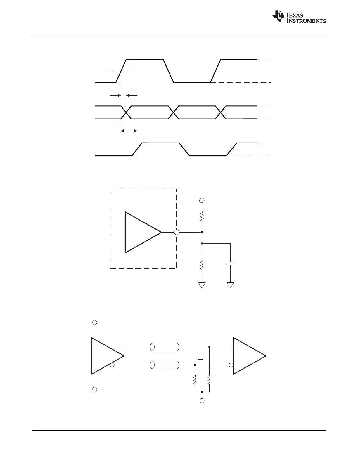
A. Output skew, t
B. Pluse skew, t
is calculated as the greater of:
The difference between the fastest and the slowest tpd(LH)n (n = 0...4)
The difference between the fastest and the slowest tpd(HL)n (n = 0...4)
the low-to-high (tpd(LH)) propagation delays when a single switching input causes one or more outputs to switch,
t
= |tpd(HL) – tpd(LH) |. Pulse skew is sometimes refered to as pulse width distortion or duty cycle skew.
sk(p)
sk(o),
, is calculated as the magnitude of the absolute time difference between the high-to-low (tpd(HL)) and
sk(p)
Figure 10. Output Skew
Product Folder Links: CDCM7005
Submit Documentation FeedbackCopyright © 2005–2017, Texas Instruments Incorporated
13
S0078-01
V
CC
V
EE
VT =V
CC
– 2V
CDCM7005
Driver
LVPECL
Receiver
Z =50OW
50W50W
Z =50OW
Yx
Yx
S0079-01
CDCM7005
LVCMOS
1kW
1kW
10pF
Y3
T0060-01
V
IH
V
IL
V
OH
V
OL
V
OH
V
OL
REF_IN
YxB
YxA
LVCMOS
LVPECL
t
pho LVPECL
50%V
CC
t
pho LVCMOS
CDCM7005
SCAS793G –JUNE 2005–REVISED AUGUST 2017
Parameter Measurement Information (continued)
www.ti.com
Figure 11. Phase Offset
14
Figure 12. LVCMOS Output Loading During Device Test
Figure 13. LVPECL Output Loading During Device Test
Submit Documentation Feedback Copyright © 2005–2017, Texas Instruments Incorporated
Product Folder Links: CDCM7005

CDCM7005
www.ti.com
SCAS793G –JUNE 2005–REVISED AUGUST 2017
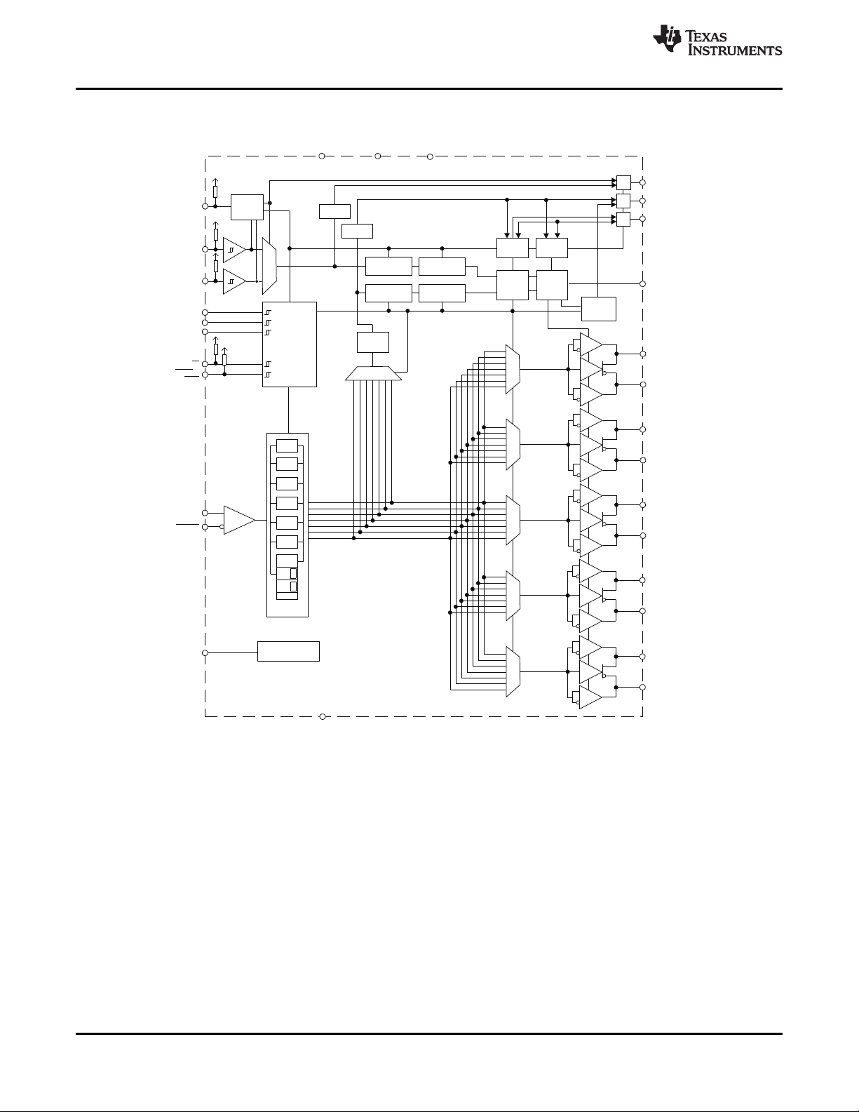
9 Detailed Description
9.1 Overview
The CDCM7005 is a high-performance, low phase noise and low skew clock synchronizer that synchronizes a
VCXO or VCO frequency to one of the two reference clocks. VC(X)O_IN clock operates up to 2.2 GHz. Through
the selection of external VC(X)O and loop filter components, the PLL loop bandwidth and damping factor can be
adjust to meet different system requirements.
The CDCM7005 can lock to one of two reference clock inputs (PRI_REF and SEC_REF), supports frequency
hold-over mode and fast-frequency-locking for fail-safe and increased system redundancy. The outputs of the
CDCM7005 are user definable and can be any combination of up to five LVPECL outputs or up to 10 LVCMOS
outputs. The LVCMOS outputs are arranged in pairs (Y0A:Y0B, Y1A:Y1B, …), so that each pair has the same
frequency. But each output can be separately inverted and disabled. The built in synchronization latches ensure
that all outputs are synchronized for low output skew.
CDCM7005 is programmable through SPI (3-wire serial peripheral interface). SPI allows individually control of
the device settings.
The device operates in 3.3-V environment and is characterized for operation from –40°C to 85°C.
Product Folder Links: CDCM7005
Submit Documentation FeedbackCopyright © 2005–2017, Texas Instruments Incorporated
15
B0057-01
PECL
to
LVCMOS
Progr.Delay
N
PECL
INPUT
CTRL_LE
CTRL_DATA
CTRL_CLK
VCXO_IN
VCXO_IN
CP_OUT
PLL_LOCK
STATUS_VCXO/
STATUS_REF/
PRI_SEC_CLK
I_REF_CP
RESET or
HOLD
PD
BiasGenerator
V 1.3VCC–
VBB
VCC_CPVCC AVCC
GND
PRI_REF
SEC_REF
REF_SEL
RE F_MU X
LVCMOS
FB_MUX
LV
CMOS
Y0B
Y0A
LV
CMOS
LV
PECL
LV
CMOS
Y1B
Y1A
LV
CMOS
LV
PECL
LV
CMOS
Y2B
Y2A
LV
CMOS
LV
PECL
LV
CMOS
Y3B
Y3A
LV
CMOS
LV
PECL
LV
CMOS
Y4B
Y4A
LV
CMOS
LV
PECL
SPILOGIC
Manual&
Automatic
CLKSelect
Current
Reference
Reference
Clock
SelectedREFSignal
Progr.Divider
N 2
12
P Divider
÷3
÷4
÷6
/8
÷8
÷16
÷1
÷2
÷4
÷8
90
o
90
o
LOCK
Charge
Pump
PFD
Y0_MUX
HOLD
P16-Div
freq.Detect
>2Mhz
freq.Detect
>2Mhz
Progr.Delay
M
Progr.Divider
M2
10
Feedback
Clock
Y1_MUXY2_MUXY3_MUX
Y4_MUX
CDCM7005
SCAS793G –JUNE 2005–REVISED AUGUST 2017
9.2 Functional Block Diagram
www.ti.com
9.3 Feature Description
9.3.1 Automatic/Manual Reference Clock Switching
The CDCM7005 supports two reference clock inputs, the primary clock input, PRI_REF, and the secondary clock
input, SEC_REF. The clocks can be selected manually or automatically. The respective mode is selected by the
dedicated SPI register bit (Word 0, Bit 30).
In the manual mode, the external REF_SEL signal selects one of the two input clocks:
REF_SEL [1] -> primary clock is selected
REF_SEL [0] -> secondary clock is selected
In the automatic mode, the primary clock is selected by default even if both clocks are available. In case the
primary clock is not available or fails, then the input switches to the secondary clock as long until the primary
clock is back. Figure 14 shows the automatic clock selection.
16
Submit Documentation Feedback Copyright © 2005–2017, Texas Instruments Incorporated
Product Folder Links: CDCM7005

T0063-01
PRI_REF
SEC_REF
Internal
ReferenceClock
YxOutput
PRI_SEC_CLK
1
1
2
2
3
4
PrimaryClock
SecondaryClock
PrimaryClock
T0062-01
PRI_REF
SEC_REF
STATUS_REF
PRI_SEC_CLK
1
2
1 2
3
4
Internal
ReferenceClock
PrimaryClock
SecondaryClock
PrimaryClock
www.ti.com
Feature Description (continued)
NOTE: PRI_REF is the preferred clock input.
Figure 14. Behavior of STATUS_REF and PRI_SEC_CLK
CDCM7005
SCAS793G –JUNE 2005–REVISED AUGUST 2017
In the automatic mode, the frequencies of both clock signals have to be similar, but may differ by up to 20%. The
phase of the clock signal can be any.
The clock input circuitry is design to suppress glitches during switching between the primary and secondary clock
in the manual and automatic mode. This avoids an undefined switching of the following circuitries.
The phase of the output clock slowly follows the new input phase. There will be no phase-jump at the output.
How quick the phase adjustment is done depends on the selected loop parameter, i.e., at a loop bandwidth of
<100 Hz; the phase adjustment can take several ms. There is no phase build-out function supported (like in
SONET/SDH applications).
Figure 15. Phase Approach of Output to New Reference Clock
9.3.2 PLL Lock for Analog and Digital Detect
The CDCM7005 supports two PLL lock indications: the digital lock signal or the analog lock signal. Both signals
indicate logic high-level at PLL_LOCK if the PLL locks according the selected lock condition.
Product Folder Links: CDCM7005
Submit Documentation FeedbackCopyright © 2005–2017, Texas Instruments Incorporated
17

T0064-01
t
(lockdetect)
SelectedREFatPFD
(clockfedthroughMDividerandMDelay)
VCXO_INatPFD
(clockfedthroughNDividerandNDelay)
CDCM7005
SCAS793G –JUNE 2005–REVISED AUGUST 2017
www.ti.com
Feature Description (continued)
9.3.2.1 PLL Lock/Out-of-Lock Definition
The PLL is locked (set high), if the rising edge of the Reference Clock (PRI_REF or SEC_REF clock) and
Feedback Clock (VCXO_IN clock) at the PFD (phase frequency detect) are inside a predefined lock detect
window, or if no frequency offset appears, for a pre-defined number of successive clock cycles.
The PLL is out-of-lock (set low), if the rising edge of the Reference Clock (PRI_REF or SEC_REF clock) and
Feedback Clock (VCXO_IN clock) at the PFD are outside the predefined lock detect window or if a frequency
offset appears.
Both, the lock detect window and the number of successive clock cycles are user definable (Word 3, Bit 2-6).
Figure 16. Lock Detect Window
The lock detect window describes the maximum allowed time difference for lock detect between the rising edge
of PRI_REF or SEC_REF and VCXO_IN. The time difference is detected at the phase frequency detector. The
rising edge of PRI_REF or SEC_REF is taken as reference. The rising edge of VCXO_IN is outside the lock
detect window if there is a phase displacement of more than +0.5 × t
(lockdetect)
or -0.5 x t
(lockdetect)
.
18
Submit Documentation Feedback Copyright © 2005–2017, Texas Instruments Incorporated
Product Folder Links: CDCM7005

Power_Down
Lock_Out
Lock_In
100 Am
(Lock)
100 Am
(Out-of-Lock)
80kW
5pF
C
PLL_LOCK
Output
Lock
t
V = 0.55 V
high CC
V
CC
V = 0.35 V
low CC
Out-of-Lock
V
Out
V = 1/C I t
Out
´ ´
Example:
for I = 110 A, C = 10nF, V = 3.3 V,m
CC
and V = V = 0.55 Vcc = 1.8V
high out
´
t = 164 s³ m
CDCM7005
Power_Down
Lock_Out
Lock_In
80kW
5pF
PLL_LOCK
Output
CDCM7005
Lock
t
Digital Lock Detection
V = 0.55 V
high CC
V = 0.35 V
low CC
Out-of-Lock
V
Out
CDCM7005
www.ti.com
SCAS793G –JUNE 2005–REVISED AUGUST 2017
Feature Description (continued)
9.3.2.2 Digital vs Analog Lock
Figure 17 and Figure 18 show the circuit for the digital and analog lock. The analog lock operates with an
external load capacitor.
When selecting the digital PLL lock option, PLL_LOCK will possibly jitter several times between lock and out of
lock until a stable lock is detected. A single low-to-high step can be reached with a wide lock detect window and
high number of successive clock cycles. PLL_LOCK returns to out of lock if just one cycle is outside the lock
detect window or a frequency offset occurs.
Figure 17. Digital Lock-Detect
When selecting the analog PLL Lock option, the high-pulses load the external capacitor via the internal 110-µA
current source until logic high-level is reached. Therefore, more time is needed to detect logic high level, but
jittering of PLL_LOCK will be suppressed in case of digital lock. The time PLL_LOCK needs to return to out of
lock depends on the level of V
, when the current source starts to unload the external capacitor.
Out
Figure 18. Analog Lock-Detect
Product Folder Links: CDCM7005
Submit Documentation FeedbackCopyright © 2005–2017, Texas Instruments Incorporated
19

B0058-01
PECL
Input
VCXO_IN
VCXO_IN
P Divider
÷3
÷4
÷6
/8
÷8
÷16
÷1
÷2
÷4
÷8
90
o
90
o
P16-Div
CDCM7005
SCAS793G –JUNE 2005–REVISED AUGUST 2017
www.ti.com
Feature Description (continued)
9.3.3 Differential LVPECL Outputs and Single-Ended LVCMOS Outputs
The CDCM7005 supports up to 5 × LVPECL outputs or 10 × LVCMOS/LVTTL outputs or any combination of
these. The single-ended LVCMOS outputs are arranged in pairs which mean both outputs of a LVCMOS pair
have the same frequency but can separately be disabled or inverted. The power up output arrangement is five
LVPECL (default setting).
The LVPECL outputs are designed to terminate in to a 50-Ω load to VCC– 2 V. The LVCMOS outputs supports
the standard LVCMOS load (see Figure 12). The LVPECL and LVCMOS outputs can be enabled (normal
operation) or disabled (3-state).
In addition, the output phase can be shifted by 90 degrees when using the additional div-by-4 or div-by-8 mode
of the P16-Div (see Figure 19). In the default mode (after power up), the div-by-16 mode of the P16-Div is active.
To change it to a 90 degree phase shift, bit 30 or bit 31 of word 1 has to be programmed accordingly. The P 16Div has to be selected via the dedicated YxMUX to obtain the 90 degree phase shift. The outputs are switched in
pairs. When selecting the 90 degree phase shift mode, the div-by-16 functions will no longer be available. The 90
degree phase shifted signal is lagging to the non-shifted signal.
Figure 19. 90 Degree Phase Shift Option of P-Divider
Figure 20 shows the LVCMOS and LVPECL output signal when 90 degree phase shift is on.
20
Submit Documentation Feedback Copyright © 2005–2017, Texas Instruments Incorporated
Product Folder Links: CDCM7005

T0065-01
ReferenceClock
VCXOClock
Y-Outputdiv4
Y-Outputdiv4
(90degshift)
Y-Outputdiv8
(90degshift)
90deg
90deg
Y-Outputdiv8
90deg
90deg
LVCMOSOutputs LVPECL Outputs
www.ti.com
Feature Description (continued)
CDCM7005
SCAS793G –JUNE 2005–REVISED AUGUST 2017
Figure 20. Output Switching Diagram
In addition, the LVCMOS supports disabled-to-low and 180 degree output phase shift for each output individually.
When selecting the 180 degree phase shift together with the 90 degree phase shift, the respective outputs has a
total phase shift of 270 degree (see Table 1).
Table 1. LVCMOS Phase Shift Options
PHASE P-DIVIDER 180° PHASE-SHIFT P16-DIV - FUNCTION
0° Any P-Divider No div-by-16
90° P16-Div No div-by-4 or div-by-8
180° Any P-Divider Yes div-by-16
270° P16-Div Yes div-by-4 or div-by-8
If the P16-Div is selected by the FB_MUX and div-by-4 or div-by-8 is active, the 90 degree phase shifted clock
will be synchronized to PRI_REF or SEC_REF. This means all outputs Yxx, which are switched to div-by-4 or
div-by-8, are in phase to PRI_REF or SEC_REF. All other outputs are 90 degree phase shifted with leading
phase.
Product Folder Links: CDCM7005
Submit Documentation FeedbackCopyright © 2005–2017, Texas Instruments Incorporated
21

CDCM7005
SCAS793G –JUNE 2005–REVISED AUGUST 2017
www.ti.com
9.3.4 Frequency Hold-Over Mode
The HOLD function is a useful feature which helps the designer to improve the system reliability. The HOLD
function holds the output frequency in case the input reference clock fails or is disrupted. During HOLD, the
charge pump is switched off (3-state) freezing the last valid output frequency. The hold function will be released
after a valid reference clock is back. For proper HOLD function, the analog PLL lock detect mode has to be
active.
The following register settings are involved with the HOLD function:
• Lock Detect Window (Word 3, Bit 2, 3, 6): Defines the window in ns inside the lock is valid. The size is
3.5 ns, 8.5 ns, 18.5 ns, or a certain frequency offset. Lock is set if reference clock and the feedback clock are
inside this predefined lock-detect window for a pre-selected number of successive cycles or if no frequency
offset appears.
• Out-of-Lock: Defines the out-of-lock condition: If the reference clock and the feedback clock at the PFD are
outside the predefined Lock Detect Window or if a certain frequency offset occurs.
• Cycle-Slip (Word 3, Bit 6): A Frequency offset occurs if a certain frequency offset between reference
frequency and feedback frequency (VCXO) at PFD input is detected. The minimum detectable frequency
offset depends on the device setting and can be calculated:
f
offsetPDF
= f
PFD
– 1/(1/f
PFD
+ PWD)
where
• f
(fFB)
• f
• PWD = PFD Pulse Width Delay (1)
= detectable frequency offset at PFD between the reference frequency (f
offsetPFD
= frequency at phase-frequency detection circuitry
PFD
) and feedback frequency
REF
• Number of Clock Cycles (Word 3, Bit 4, 5): Defines the number of successive PFD cycles which have to
occur inside the lock window to set Lock detect. This applies not for out-of-lock condition.
• Hold-Function (Word 3, Bit 9): Selects HOLD function (see more details below).
• Hold-Trigger (Word 3, Bit 11): Defines whether the HOLD function is always activated (Bit 11 = [1]) or whether
it is dependent on the state of the analog PLL lock detect output (Bit 11 = [0]). In the latter case, HOLD is
activated, if lock is set (high) and de-activated if Lock is reset (low).
• Analog PLL Lock Detect (Word 1, Bit 29): Analog lock output charges or discharges an external capacitor with
every valid lock cycle. The time constant for Lock detect can be set by the value of the capacitor.
The CDCM7005 supports two types of HOLD functions, one external controllable HOLD mode and one internal
mode, HOLD.
With the external HOLD function the charge pump can directly be switched into 3-state (pin H8 [BGA] or pin 14
[QFN] can be programmed for HOLD [Word 2, Bit 29]). This function is also available via SPI register (Word 2,
Bit 31).
If logic low is applied to the HOLD pin, the charge pump will be switched to 3-state. After the HOLD pin is
released, the charge pump is switched back in to normal operation with the next valid reference clock cycle at
PRI_REF or SEC_REF and the next valid feedback clock cycle at the PFD. During HOLD, the P divider and all
outputs Yx are at normal operation.
HOLD-Over-Function: The PLL has to be in lock to start the HOLD function. It switches the charge pump in to 3State when an out-of-lock event occurs. It leaves the 3-state charge pump state when the reference clock is
back. Then it starts a locking sequence of 64 cycles before it goes back to the beginning of the HOLD-over loop.
The dedicated looking sequence and a digital phase alignment enable a fast lock.
22
Submit Documentation Feedback Copyright © 2005–2017, Texas Instruments Incorporated
Product Folder Links: CDCM7005

F0004-01
No
No
No
PLL
Out-of-Lock?
PLL-Lock
Output
Set?
3-State Charge-Pump
Reference Clock
Back?
64 PFD
Lock-Cycles
Yes
Yes
Yes
Charge-Pump is switched into 3-State.
P-divider and Yx output are at normal operation.
The Charge-Pump remains in 3-State
until the Reference Clock is back. The 1st
valid Reference Clock at the PFD releases
the Charge-Pump.
The PLL acquire 64 lock cycles to phase
align to the input clock.
Frequency Hold-Over Function works in
combination with the Analog Lock-Detect
function only!
Start
PLL is out-of-lock if the phase
difference of Reference Clock and
Feedback Clock at PFD are outside the
predefined Lock-Detect-Window or if a
frequency offset occurs.
PLL has to be in LOCK to start
HOLD-Function.
(The Analog Lock output is not reset by the first Out-of-
Lock event. It stays ‘High’ depending on the analog time
delay (output C-load). The time delay must be long enough
to assure proper HOLD function)
(The ‘PLL-Lock Output Set?’ enquiry can be bypassed by
setting the HOLDTR bit to [1] (Word 3, Bit 11)
www.ti.com
CDCM7005
SCAS793G –JUNE 2005–REVISED AUGUST 2017
9.3.5 Charge Pump Preset to VCC_CP/2
The preset charge pump to VCC_CP/2 is a useful feature to quickly set the center frequency of the VC(X)O after
powerup or reset. The adequate control voltage for the VC(X)O will be provided to the charge-pump output by an
internal voltage divider of 1 kΩ/1 kΩ to VCC_CP and GND (VCC_CP/2).
This feature helps to get the initial frequency accuracy, i.e. required at CPRI (Common Public Radio Interface) or
OBSAI (Open Base Station Architecture Initiative).
The preset charge pump to VCC_CP/2 can be set and reset by SPI register (word 2, bit 3). This feature must be
disabled for PLL locking.
Figure 21. Frequency HOLD-Over Function
Product Folder Links: CDCM7005
Submit Documentation FeedbackCopyright © 2005–2017, Texas Instruments Incorporated
23

T0076-01
PFDPulse
WidthDelay
PFDPulse
WidthDelay
0V
V
CC
PRI_REForSEC_REF
ClockFedThroughthe
MDividerandDelay
VCXO_INClockFedThrough
theNDividerandDelay
CP_DIR(Bit2ofWord2=0,
DefaultState)
CP_DIR(Bit2ofWord2=1)
V (InternalSignal)
(PFD1)
V (InternalSignal)
(PFD2)
CDCM7005
SCAS793G –JUNE 2005–REVISED AUGUST 2017
www.ti.com
9.3.6 Charge Pump Current Direction
The direction of the charge pump (CP) current pulse can be changed by the SPI register (word 2, bit 2). It
determines in which direction the CP current regulates (reference clock leads to feedback clock). Most
applications use the positive CP output current (power-up condition) because of the use of a passive loop filter.
The negative CP current is useful when using an active loop filter concept with inverting operational amplifier.
Figure 22 shows the internal PFD signal and the corresponding CP current.
NOTE: The purpose of the PFD pluse width delay is to improve spurious suppression.
9.4 Device Functional Modes
Device starts up in normal operational mode and might enter RESET or Power-Down modes by external signal
or by writing to internal SPI registers.
CDCM7005 enters the Power Down mode if PD signal is activated (LOW) or by writing to the corresponding bit in
the configuration registers R02[28]. this power-down mode resets M- and N-Divider, 3-states charge pump,
STATUS_REF, or PRI_SEC_CLK pin, STATUS_VCXO or I_REF_CP pin, PLL_LOCK pin, VBB pin and all Yx
outputs. This mode resets all the SPI registers to the default value. In this mode maximum current consumption
is 300 uA.
CDCM7005 enters the RESET mode when RESET pin is activated (LOW), given that this pin is configured as
RESET by R02[29], or by writing to the corresponding bit R02[30].In case of RESET, the charge pump (CP) is
switched to 3-state and all counters (N, M, P) are reset to zero (the initial divider settings are maintained in SPI
registers). The LVPECL outputs are static low and high respectively and the LVCMOS outputs are all low or high
if inverted. Note that RESET is not edge triggered and should have a pulse duration of at least 5 ns.
Figure 22. Charge Pump Current Direction (VCXO and VCO Support)
24
Submit Documentation Feedback Copyright © 2005–2017, Texas Instruments Incorporated
Product Folder Links: CDCM7005

T0061-01
CTRL_DATA
CTRL_LE
CTRL_CLK
t
su5
t
su6
Bit31(MSB)
Bit2 Bit1
Bit0
Bit30
t
4
t
7
t
3
t
su1
t
h2
CDCM7005
www.ti.com
SCAS793G –JUNE 2005–REVISED AUGUST 2017
9.5 Programming
9.5.1 SPI Control Interface
The serial interface of the CDCM7005 is a simple SPI-compatible interface for writing to the registers of the
device and consists of three control lines: CTRL_CLK, CTRL_DATA, and CTRL_LE. There are four 32-bit wide
registers, which can be addressed by the two LSBs of a transferred word (bit 0 and bit 1). Every transmitted word
must have 32 bits, starting with MSB first. Each word can be written separately. Bit 7, 8, 10, and Bit 12 to 31 of
Word 3 are reserved for factory test purposes and must be filled with zeros. The transfer is initiated with the
falling edge of CTRL_LE; as long as CTRL_LE is high, no data can be transferred. During CTRL_LE, low data
can be written. The data has to be applied at CTRL_DATA and has to be stable before the rising edge of
CTRL_CLK. The transmission is finished by a rising edge of CTRL_LE. With the rising edge of CTRL_LE, the
new word is asynchronously transferred to the internal register (e.g., N, M, P, ...). Each word has to be
separately transmitted by this procedure. Unused or floating inputs must be tied to proper logic level. A 20kΩ or
larger pull−up resistor to VCC is recommended.
Figure 23. Timing Diagram SPI Control Interface
The SPI serial protocol accepts word Write operation only. There is neither a read, acknowledge, nor a
handshake operation.
The following four words include the register settings of the programmable functions of the CDCM7005. It can be
modified to the customer application by changing one or more bits. It comes up with a default register setting
after power up or if the power down (PD) control signal is applied. The default setting is shown in column five of
the following words.
It is recommended to program Word 0, Word 1, Word 2, and Word 3 right after power up and PD becomes
HIGH.
A low active function is shown as [0] and a high active function is shown as [1].
Submit Documentation FeedbackCopyright © 2005–2017, Texas Instruments Incorporated
Product Folder Links: CDCM7005
25

CDCM7005
SCAS793G –JUNE 2005–REVISED AUGUST 2017
www.ti.com
Programming (continued)
Table 2. Word 0
PIN AFFECTED
BGA QFN
(2)
POWER UP
CONDITION
0 A1, B1 36, 37
0 C8 23
BIT BIT NAME DESCRIPTION/FUNCTION
0 C0 Register Selection 0
1 C1 Register Selection 0
2 M0 Reference Divider M Reference Divider M Bit 0 1
3 M1 Reference Divider M Bit 1 1
4 M2 Reference Divider M Bit 2 1
5 M3 Reference Divider M Bit 3 1
6 M4 Reference Divider M Bit 4 1
7 M5 Reference Divider M Bit 5 1
8 M6 Reference Divider M Bit 6 1
9 M7 Reference Divider M Bit 7 0
10 M8 Reference Divider M Bit 8 0
11 M9 Reference Divider M Bit 9 0
12 N0 VC(X)O Divider N
13 N1 VCXO Divider N Bit 1 1
14 N2 VCXO Divider N Bit 2 1
15 N3 VCXO Divider N Bit 3 1
16 N4 VCXO Divider N Bit 4 1
17 N5 VCXO Divider N Bit 5 1
18 N6 VCXO Divider N Bit 6 1
19 N7 VCXO Divider N Bit 7 0
20 N8 VCXO Divider N Bit 8 0
21 N9 VCXO Divider N Bit 9 0
22 N10 VCXO Divider N Bit 10 0
23 N11 VCXO Divider N Bit 11 0
24 DLYM0 Progr. Delay M Reference Phase Delay M Bit 0 0
25 DLYM1 Reference Phase Delay M Bit 1 0
26 DLYM2 Reference Phase Delay M Bit 2 0
27 DLYN0 Progr. Delay N Feedback Phase Delay N Bit 0 0
28 DLYN1 Feedback Phase Delay N Bit 1 0
29 DLYN2 Feedback Phase Delay N Bit 2 0
30 MANAUT Manual or Auto Ref. Manual Reference Clock Selection [0]
31 REFDEC Freq. Detect Reference Frequency Detection on [0], off [1]
(1) The frequency applied to the Divider N must be smaller than 300 MHz. A sufficient P Divider must be selected with the FB_MUX to
maintain this criteria.
(2) If set to low, STATUS_REF will be in normal operation. If set to high, STATUS_REF will be high, even if no valid clock is
detected (<2 MHz). This is useful for reference inputs frequencies less than 2 MHz where the frequency detection circuitry normally
resets the STATUS_REF signal to low.
(1)
VCXO Divider N Bit 0 1
Automatic Reference Clock Selection [1]
26
Submit Documentation Feedback Copyright © 2005–2017, Texas Instruments Incorporated
Product Folder Links: CDCM7005

CDCM7005
www.ti.com
SCAS793G –JUNE 2005–REVISED AUGUST 2017
Table 3. Word 1
BIT BIT NAME DESCRIPTION/FUNCTION
POWER UP
CONDITION
0 C0 Register Selection 1
1 C1 Register Selection 0
2 OUTSEL0 Output (Yx)
Signaling Selection
3 OUTSEL1 For Outputs Y1A, Y1B:
For Output Y0A, Y0B:
LVPECL = enabled [1]; LVCMOS = enabled [0];
1 F1, G1 46, 47
1 H2, H3 3, 4
LVPECL = enabled [1]; LVCMOS = enabled [0];
4 OUTSEL2 For Outputs Y2A, Y2B:
1 H4, H5 7, 8
LVPECL = enabled [1]; LVCMOS = enabled [0];
5 OUTSEL3 For Outputs Y3A, Y3B:
1 H6, H7 11, 12
LVPECL = enabled [1]; LVCMOS = enabled [0];
6 OUTSEL4 For Outputs Y4A, Y4B:
1 G8, F8 16,17
LVPECL = enabled [1]; LVCMOS = enabled [0];
7 OUT0A0 Output Y0 Mode Output Y0A Mode Bit 0 0 F1 46
8 OUT0A1 Output Y0A Mode Bit 1 0 F1 46
9 OUT0B0 Output Y0B Mode Bit 0 0 G1 47
10 OUT0B1 Output Y0B Mode Bit 1 0 G1 47
11 OUT1A0 Output Y1 Mode Output Y1A Mode Bit 0 0 H2 3
12 OUT1A1 Output Y1A Mode Bit 1 0 H2 3
13 OUT1B0 Output Y1B Mode Bit 0 0 H3 4
14 OUT1B1 Output Y1B Mode Bit 1 0 H3 4
15 OUT2A0 Output Y2 Mode Output Y2A Mode Bit 0 0 H4 7
16 OUT2A1 Output Y2A Mode Bit 1 0 H4 7
17 OUT2B0 Output Y2B Mode Bit 0 0 H5 8
18 OUT2B1 Output Y2B Mode Bit 1 0 H5 8
19 OUT3A0 Output Y3 Mode Output Y3A Mode Bit 0 0 H6 11
20 OUT3A1 Output Y3A Mode Bit 1 0 H6 11
21 OUT3B0 Output Y3B Mode Bit 0 0 H7 12
22 OUT3B1 Output Y3B Mode Bit 1 0 H7 12
23 OUT4A0 Output Y4 Mode Output Y4A Mode Bit 0 0 G8 16
24 OUT4A1 Output Y4A Mode Bit 1 0 G8 16
25 OUT4B0 Output Y4B Mode Bit 0 0 F8 17
26 OUT4B1 Output Y4B Mode Bit 1 0 F8 17
27 SREF Status Ref. Displays the status of the reference clock at the
0 C8 23
STATUS_REF output [0]
Displays the selected clock (high for PRI_REF and
low for SEC_REF clock) at the STATUS_REF
output [1]
28 SXOIREF Status VCXO or
I_REF_CP
Selects STATUS_VCXO [0] 0 D8, A8 22, 25
Selects I_REF_CP [1] which enable external
reference resistor used for charge pump current and
analog PLL lock detect output current.
29 ADLOCK Analog or Digital
Lock
30 90DIV4 90 degree shift div-490 degree output phase shift in div-4 mode on [1];
31 90DIV8 90 degree shift div-890 degree output phase shift in div-8 mode on [1];
Selects Digital PLL_LOCK [0]
Selects Analog PLL_LOCK [1]
(1)
off [0]
(1)
off [0]
0 A8 25
0 Yx Yx
0 Yx Yx
(1) The P 16-Div has to be selected to obtain the 90 degree phase shift. If bit 30 or bit 31 is set, the Div-by-16 mode is no longer available.
The outputs are switched in pairs. Only one bit can be set at a time. If both bits set to [1] at the same time, no 90 degree phase shift
mode is selected (equal to off-mode setting).
PIN AFFECTED
BGA QFN
Product Folder Links: CDCM7005
Submit Documentation FeedbackCopyright © 2005–2017, Texas Instruments Incorporated
27

CDCM7005
SCAS793G –JUNE 2005–REVISED AUGUST 2017
Table 4. Word 2
BIT
0 C0 Register Selection 0
1 C1 Register Selection 1
2 CP_DIR CP Direction Determines in which direction CP current regulates (Reference
3 PRECP Preset charge pump output voltage to VCC_CP/2, on [1], off [0] 0 A4 31
4 CP0 CP Current CP Current Setting Bit 0 0 A4 31
5 CP1 CP Current Setting Bit 1 1 A4 31
6 CP2 CP Current Setting Bit 2 0 A4 31
7 CP3 CP Current Setting Bit 3 1 A4 31
8 PFD0 PFD Pulse
9 PFD1 PFD Pulse Width PFD Bit 1 0 A4 31
10 FBMUX0 FB_MUX Feedback MUX Select Bit 0 1
11 FBMUX1 Feedback MUX Select Bit 1 0
12 FBMUX2 Feedback MUX Select Bit 2 1
13 Y0MUX0 Y0_MUX Output Y0x Select Bit 0 1 F1, G1 46, 47
14 Y0MUX1 Output Y0x Select Bit 1 0 F1, G1 46, 47
15 Y0MUX2 Output Y0x Select Bit 2 1 F1, G1 46, 47
16 Y1MUX0 Y1_MUX Output Y1x Select Bit 0 1 H2, H3 3, 4
17 Y1MUX1 Output Y1x Select Bit 1 0 H2, H3 3, 4
18 Y1MUX2 Output Y1x Select Bit 2 1 H2, H3 3, 4
19 Y2MUX0 Y2_MUX Output Y2x Select Bit 0 1 H4, H5 7, 8
20 Y2MUX1 Output Y2x Select Bit 1 0 H4, H5 7, 8
21 Y2MUX2 Output Y2x Select Bit 2 1 H4, H5 7, 8
22 Y3MUX0 Y3_MUX Output Y3x Select Bit 0 1 H6, H7 11, 12
23 Y3MUX1 Output Y3x Select Bit 1 0 H6, H7 11, 12
24 Y3MUX2 Output Y3x Select Bit 2 1 H6, H7 11, 12
25 Y4MUX0 Y4_MUX Output Y4x Select Bit 0 1 G8, F8 16, 17
26 Y4MUX1 Output Y4x Select Bit 1 0 G8, F8 16, 17
27 Y4MUX2 Output Y4x Select Bit 2 1 G8, F8 16, 17
28 PD Power Down mode on [0], off [1] 1 Yx Yx
29 RESHOL RESET or HOLD Pin definition: RESET [0] or HOLD [1] 0 H8 14
30 RESET Resets all dividers [0] - (equal to RESET pin function) 1
31 HOLD 3-state charge pump [0] - (equal to HOLD pin function) 1 A4 31
BIT
NAME
DESCRIPTION/FUNCTION
Clock leads to Feedback Clock – see Figure 22)
– positive CP output current [0];
– negative CP output current [1];
PFD Pulse Width PFD Bit 0 0 A4 31
Width
POWER UP
CONDITIO
N
0 A4 31
PIN AFFECTED
BGA QFN
www.ti.com
28
Submit Documentation Feedback Copyright © 2005–2017, Texas Instruments Incorporated
Product Folder Links: CDCM7005

CDCM7005
www.ti.com
SCAS793G –JUNE 2005–REVISED AUGUST 2017
Table 5. Word 3
BIT
BIT
NAME
DESCRIPTION/FUNCTION
POWER UP
CONDITION
0 Register selection 1
1 Register selection 1
2 LOCKW 0 Lock Window Lock-detect window Bit 0 1 A8 25
3 LOCKW 1 Lock-detect window Bit 1 0 A8 25
4 LOCKC0 Lock Cycles Number of coherent lock events Bit 0 0 A8 25
5 LOCKC1 Number of coherent lock events Bit 1 1 A8 25
6 FOFF Frequency Offset
Frequency offset mode only for out-of-lock detection
on [1] or off [0]
(1)
0 A8 25
7 RES RESERVED 0 RES RES
8 RES RESERVED 0 RES RES
9 HOLDF HOLD Function Enables the frequency hold-over function on [1], off [0] 0
10 RESERVED 0 RES RES
(2)
0
11 HOLDTR
HOLD Trigger
Condition
HOLD function always activated [1];
Triggered by analog PLL lock detect outputs [0] (if
analog PLL Lock signal is set then HOLD is activated;
if analog PLL lock signal is reset then HOLD is de-
activated).
12 RES RESERVED 0 RES RES
13 RES RESERVED 0 RES RES
14 RES RESERVED 0 RES RES
15 RES RESERVED 0 RES RES
16 GTME General Test Mode Enable. Test Mode is only
0
enabled if this bit is set to 1.
17 RES RESERVED 0 RES RES
18 RES RESERVED 0 RES RES
19 RES RESERVED 0 RES RES
20 RES RESERVED 0 RES RES
21 RES RESERVED 0 RES RES
22 RES RESERVED 0 RES RES
23 RES RESERVED 0 RES RES
24 RES RESERVED 0 RES RES
25 RES RESERVED 0 RES RES
26 RES RESERVED 0 RES RES
27 RES RESERVED 0 RES RES
28 PFDFC PFD Frequency Control. Data provided to the PFD
are feed through to the corresponding STATUS
(3)
pins
0 D8 22
29 RES RESERVED 0 RES RES
30 RES RESERVED 0 RES RES
31 RES RESERVED 0 RES RES
(1) If Frequency offset mode only for out-of-lock detection is on, the selected lock detect window is valid for lock detect. Independent from
this, out of lock is valid if a frequency offset is detected.
(2) HOLD function always activated is recommended for test purposes only.
(3) The maximum frequency for the STATUS_VCXO pin is 100 MHz.
PIN AFFECTED
BGA QFN
Product Folder Links: CDCM7005
Submit Documentation FeedbackCopyright © 2005–2017, Texas Instruments Incorporated
29

CDCM7005
SCAS793G –JUNE 2005–REVISED AUGUST 2017
9.5.2 Functional Description of the Logic
www.ti.com
Table 6. Reference Divider M (Word 0)
M9 M8 M7 M6 M5 M4 M3 M2 M1 M0 DIV BY DEFAULT
0 0 0 0 0 0 0 0 0 0 1
0 0 0 0 0 0 0 0 0 1 2
0 0 0 0 0 0 0 0 1 0 3
0 0 0 0 0 0 0 0 1 1 4
•
•
•
0 0 0 1 1 1 1 1 1 1 128 Yes
•
•
•
1 1 1 1 1 1 1 1 0 1 1022
1 1 1 1 1 1 1 1 1 0 1023
1 1 1 1 1 1 1 1 1 1 1024
(1) If the divider value is Q, then the code will be the binary value of (Q–1).
Table 7. VC(X)O Feedback Divider N (Word 0)
N11 N10 N0 N8 N7 N6 N5 N4 N3 N2 N1 N0 DIV BY DEFAULT
0 0 0 0 0 0 0 0 0 0 0 0 1
0 0 0 0 0 0 0 0 0 0 0 1 2
0 0 0 0 0 0 0 0 0 0 1 0 3
0 0 0 0 0 0 0 0 0 0 1 1 4
•
•
•
0 0 0 0 0 1 1 1 1 1 1 1 128 Yes
•
•
•
1 1 1 1 1 1 1 1 1 1 0 1 4094
1 1 1 1 1 1 1 1 1 1 1 0 4095
1 1 1 1 1 1 1 1 1 1 1 1 4096
(1) If the divider value is Q, then the code will be the binary value of (Q–1).
(2) The frequency applied to the Divider N must be smaller than 300 MHz. A sufficient P Divider must be selected with the FB_MUX to
maintain this criteria.
(1)
(1) (2)
30
Submit Documentation Feedback Copyright © 2005–2017, Texas Instruments Incorporated
Product Folder Links: CDCM7005

www.ti.com
CDCM7005
SCAS793G –JUNE 2005–REVISED AUGUST 2017
Table 8. Output Mode Selection for LVCMOS and LVPECL Outputs: Y0A, Y0B, Y1A …Y4B (Word 1)
OUTSELx OUTxB1 OUTxB0 LVCMOS
[YxB]
LVCMOS 0 0 0 Active 0 0 Active
0 0 1 3-state 0 1 3-state
0 1 0 Inverting 1 0 Inverting
0 1 1 Low 1 1 Low
OUTSELx OUTxB1 OUTxB0 OUTxA1 OUTxA0 LVCMOS
LVPECL 1 x x x 0 Active Yx
1 x x x 1 3-state
(1) If the differential LVPECL output e.g. Y0A:Y0B is selected (bit 2 of word 1), then only bit 7 of word 1 defines the output mode for
Y0A:Y0B. The settings of bit 8, bit 9, and bit 10 of word 1 are therefore not relevant to the Y0A:Y0B. This applies for the other LVPECL
outputs as well.
Table 9. Reference Delay M (PRI_REF or SEC_REF) and Feedback Delay N (VCXO) Phase Adjustment
(Word 0)
DLYM2 / DLYN2 DLYM1 / DLYN1 DLYM0 / DLYN0 PHASE OFFSET DEFAULT
0 0 0 0 ps Yes
0 0 1 ±160 ps
0 1 0 ±320 ps
0 1 1 ±480 ps
1 0 0 ±830 ps
1 0 1 ±1130 ps
1 1 0 ±1450 ps
1 1 1 ±1750 ps
(1) If Progr. Delay M is set, all Yx outputs are lagging to the reference clock according to the value set. If Progr. If Delay N is set; all Yx
outputs are leading to the reference clock according to the value set. Above are typical values at VCC= 3.3 V, Temp = 25°C, PECLoutput relate to Div4 mode.
OUTxA1 OUTxA0 LVCMOS
(1)
[YxA]
DEFAULT
DEFAULT
[YxA]
(1)
Table 10. PFD Pulse Width Delay (Word 2)
(1)
PFD1
0 0 1.5 ns Yes
0 1 3 ns
1 0 4.5 ns
1 1 6 ns
(1) The PFD pulse width delay gets around the dead zone of the PFD transfer function and reduces phase noise and reference spurs.
(2) Typical values at V = 3.3 VCC, Temp = 25°C .
PFD0
(1)
PFD PULSE WIDTH
(1) (2)
DEFAULT
(1)
Product Folder Links: CDCM7005
Submit Documentation FeedbackCopyright © 2005–2017, Texas Instruments Incorporated
31

CDCM7005
SCAS793G –JUNE 2005–REVISED AUGUST 2017
www.ti.com
Table 11. Lock-Detect Window (Word 3)
LOCKW1 LOCKW0 PHASE-OFFSET AT PFD INPUT
0 0 3.5 ns
0 1 8.5 ns Yes
1 0 18.5 ns
1 1 Frequency offset
(2)
(1) Typical Values at VCC= 3.3 V, Temp = 25°C.
(2) The PLL is out-of-lock (PLL_LOCK set low) if a certain frequency offset between reference frequency and feedback frequency (VCXO)
at PFD input is detected. The minimum detectable frequency offset depends on the device setting and can be calculated:
(a) f
(b) f
(c) f
(d) PWD = PFD Pulse Width Delay
= f
offsetPDF
offsetPFD
= frequency at phase-frequency detection circuitry
PFD
- 1/(1/f
PFD
= detectable frequency offset at PFD between the reference frequency (f
PFD
+ PWD)
REF
(1)
) and feedback frequency (fFB)
DEFAULT
Table 12. Number of Successive Lock Events Inside the Lock Detect Window (Word 3)
LOCKC1
(1)
LOCKC0
0 0 1
0 1 16
1 0 64 Yes
1 1 256
(1) This does not apply to Out-of-Lock condition.
(1)
NO. OF SUCCESSIVE LOCK EVENTS
(1)
DEFAULT
(1)
Table 13. Charge Pump Current (Word 2)
CP3 CP2 CP1 CP0 TYPICAL CHARGE PUMP CURRENT DEFAULT
0 0 0 0 0 µA (3-state)
0 0 0 1 200 µA
0 0 1 0 400 µA
0 0 1 1 600 µA
0 1 0 0 800 µA
0 1 0 1 1 mA
0 1 1 0 1.2 mA
0 1 1 1 1.4 mA
1 0 0 0 1.6 mA
1 0 0 1 1.8 mA
1 0 1 0 2.0 mA Yes
1 0 1 1 2.2 mA
1 1 0 0 2.4 mA
1 1 0 1 2.6 mA
1 1 1 0 2.8 mA
1 1 1 1 3 mA
32
Submit Documentation Feedback Copyright © 2005–2017, Texas Instruments Incorporated
Product Folder Links: CDCM7005

CDCM7005
www.ti.com
SCAS793G –JUNE 2005–REVISED AUGUST 2017
Table 14. FB_MUX Selection (Word 2)
FBMUX2 FBMUX1 FBMUX0 SELECTED VC(X)O SIGNAL FOR THE
0 0 0 Div by 1
0 0 1 Div by 2
0 1 0 Div by 3
0 1 1 Div by 4
1 0 0 Div by 6
1 0 1 Div by 8 Yes
1 1 0 Div by 16
1 1 1 Div by 8
(1) This divider setting depends on the selected P-divider mode for the “Div-by-16” divider. In the default mode (after power up), Div-by-16
is selected. But if bit 30 or bit 31 of word 1 is set to [1], then the Div-by-4 and 90 degree phase shift or Div-by-8 and 90 degree phase
shift is selected.
PHASE DESCRIMINATOR
(1)
DEFAULT
Table 15. Yx_MUX – Output Divider Selection for Y0, Y1, Y2, Y3, Y4 (Word 2)
YxMUX2 YxMUX1 YxMUX0 SELECTED DIVIDED V(C)XO SIGNAL FOR THE
0 0 0 Div by 1
0 0 1 Div by 2
0 1 0 Div by 3
0 1 1 Div by 4
1 0 0 Div by 6
1 0 1 Div by 8 all Yx
1 1 0 Div by 16
1 1 1 Div by 8
(1) This divider setting depends on the selected P-divider mode for the “Div-by-16” divider. In the default mode (after power up), Div-by-16
is selected. But if bit 30 or bit 31 of word 1 is set to [1], then the Div-by-4 and 90 degree phase shift or Div-by-8 and 90 degree phase
shift is selected.
Yx OUTPUTS
(1)
DEFAULT
Product Folder Links: CDCM7005
Submit Documentation FeedbackCopyright © 2005–2017, Texas Instruments Incorporated
33

B0064-01
LO1
(PLL)
16-Bit
DAC
16-Bit
DAC
DAC5687
FIRFIR
DDC
DUC
RF
I
I
Q
Q
14-Bit
ADC
ADS5423
3.84MHz
VCXO
491.52MHz
61.44MHz
491.52MHz
122.88MHz
122.88MHz
Duplexer
LO1
IF1
LNA
90
0
S
PA
FIRFIR
To
BB
From
BB
GC5016
GC5016
THS4509
TRF3750
(PLL)
TRF3702
CDCM7005
CDCM7005
SCAS793G –JUNE 2005–REVISED AUGUST 2017
www.ti.com
10 Application and Implementation
NOTE
Information in the following applications sections is not part of the TI component
specification, and TI does not warrant its accuracy or completeness. TI’s customers are
responsible for determining suitability of components for their purposes. Customers should
validate and test their design implementation to confirm system functionality.
10.1 Application Information
10.1.1 Application Information on the Clock Generation for Interpolating DACs With the CDCM7005
The CDCM7005, with its specified phase noise performance, is an ideal sampling clock generator for high speed
ADCs and DACs. The CDCM7005 is especially of interest for the new high speed DACs, which have integrated
interpolation filter. Such DACs achieve sampling rates up to 500 MSPS. This high data rate can typically not be
supported from the digital side driving the DAC (e.g., DUC, digital up-converter). Therefore, one approach to
interface the DUC to the DAC is the integration of an interpolation filter within the DAC to reduce the data rate at
the digital input of the DAC. In 3G systems, for example, a common sampling rate of a high speed DAC is
491.52 MSPS. With a four times interpolation of the digital data, the required input data rate results into
122.88 MSPS, which can be supported easily from the digital side. The DUC GC5016, which supports up to four
WCDMA carriers, provides a maximum output data rate of 150 MSPS. An example is shown in Figure 24, where
the CDCM7005 supplies the clock signal for the DUC/DDC and ADC/DAC.
34
Figure 24. CDCM7005 as a Clock Generator for High-Speed ADCs and DACs
Submit Documentation Feedback Copyright © 2005–2017, Texas Instruments Incorporated
Product Folder Links: CDCM7005

CDCM7005
www.ti.com
SCAS793G –JUNE 2005–REVISED AUGUST 2017
Application Information (continued)
The generation of the two required clock signals (data input clock, clock for DAC) for such an interpolating DAC
can be done in different ways. The recommended way is to use the CDCM7005, which generates the fast
sampling clock for the DAC from the data input clock signal. The DAC5687 demands that the edges of the two
input clocks must be phase aligned within ±500 ps for latching the data properly. This phase alignment is well
achieved with the CDCM7005, which assures a maximum skew of 70 ps of the different different outputs to each
other.
10.1.1.1 AC-Coupled Interface to ADC/DAC
Another advantage of this clock solution is that the ADC or DAC can be driven directly in an ac-coupling interface
as shown in Figure 25, with an external termination in a differential configuration. There is no need for a
transformer to generate a differential signal from a single-ended clock source.
Figure 25. Driving DAC or ADC With PECL Output of the CDCM7005
10.1.2 Phase Noise Table 16. Phase Noise Performance
PARAMETER
phn10 Phase noise at 10 Hz
phn100 Phase noise at 100 Hz –125 –97 –116 –116 dBc/Hz
phn1k Phase noise at 1 kHz –134 –117 –140 –140 dBc/Hz
phn10k Phase noise at 10 kHz –136 –138 –153 –152 dBc/Hz
phn100k Phase noise at 100 kHz –138 –148 –156 –153 dBc/Hz
phn1Mk Phase noise at 1 MHz –144 –148 –156 –153 dBc/Hz
phn10M Phase noise at 10 MHz –144 –148 –156 –153 dBc/Hz
PLL STABILIZATION TIME
tstabi PLL stabilization time
(1) Output phase noise is dependent on the noise of the REF_IN clock and VCXO clock noise floor. The phase noise performance of the
BGA and the QFN package is equal. The phase noise measurements were taken with the CDCM7005 EVM and CDCM7005 SPI default
settings.
(2) The typical stabilization time is based on the above application example. The stabilization criterion was a stable high level of
PLL_LOCK.
(3) For further explanations, as well as phase noise/jitter test results using various VCXOs, see application note SCAA067.
(1)
(3)
TEST CONDITIONS
Y = 30.72 MHz; f
kHz, Loop BW = 20 Hz,
Feedback Divider = 8 x 128
(N x P), f
M-Divider = 128, ICP= 2 mA
Y = 30.72 MHz, f
kHz, Loop BW = 20 Hz,
Feedback Divider = 8 x 128
(N x P), f
M-Divider = 128, ICP= 2 mA
REF_IN
REF_IN
= 200
PFD
= 30.72 MHz,
= 200
PFD
= 30.72 MHz,
REF_IN PHASE
NOISE
AT 30.72 MHz
–109 –75 –104 –100 dBc/Hz
VCXO PHASE
NOISE
AT 245.76 MHz
Yx PHASE NOISE
AT 30.72 MHz
LVCMOS LVPECL
(2)
TYP
TYP
400 ms
UNIT
(2)
Product Folder Links: CDCM7005
Submit Documentation FeedbackCopyright © 2005–2017, Texas Instruments Incorporated
35

CDCM7005
SCAS793G –JUNE 2005–REVISED AUGUST 2017
www.ti.com
10.1.3 In-Band Noise Performance Table 17. CDCM7005 In-Band Noise
PARAMETER TEST CONDITIONS MIN TYP MAX UNIT
pn
pn
pn
(1) The synthesizer phase noise floor can be estimated by measuring the in-band noise at the output of the CDCM7005 and subtracting
(2) The in-band noise can also be normalized to a comparison frequency of 1 Hz. The resulting phase noise floor is: pnfloor = PNmeasured
In-band phase noise test conditions
in-band
Phase noise floor at 400 kHz f
f400
noise – 20log(feedback div)
Phase noise floor at 1 Hz f
f1
noise – 20log(feedback div) – 10log(f
(1)
PFD
, in-band
PFD
, in-band
PFD
Y = 900 MHz, f
BW = 27 kHz, Feedback Divider = 8 x 282
(2)
)
(N x P), f
3 mA
REF_IN
= 400 kHz, Loop
PFD
= 10 MHz; M-Divider = 25, ICP=
–95 dBc/Hz
–162 dBc/Hz
–218 dBc/Hz
20log(Feedback Divider) N (in case of CDCM7005 it is the N+P divider). The calculated phase noise floor still based on the PFD update
frequency, in the above specification, is 400 kHz.
- 20log(N+P) - 10log(f
where:
PFD
)
pnNfloor = normalized phase noise floor in dBc/Hz
PNmeasured = in-band phase noise measurement in dBc/Hz
20log(N+P) = divider ratio of feedback loop
10log(f
) = PFD update frequency in Hz
PFD
36
Submit Documentation Feedback Copyright © 2005–2017, Texas Instruments Incorporated
Product Folder Links: CDCM7005

S0082-01
VCXO
Low-PassFilter
CDCM7005
245.76MHz
Gain=21.3kHz/V
PECL_OUT_B
PRI_REF
VCXO_IN
YnA
YnB
VCXO_IN
CTRL_DATA
CTRL_LE
CTRL_CLK
V_CTRL
CP_OUT
PLL_LOCK
STATUS_REF
STATUS_VCXO
PECL_OUT
SPI
V
OC
V
OC
R
130W
R
82W
R
150W
R
50W
R
82W
R
150W
R
50W
R2
160W
R
130W
R1
4.7kW
C2
100nF
C1
22 Fm
10nF
10nF
C3
100nF
Measurement
Equipment
PhaseNoiseReferenceCircuit(SeetheEVM)
www.ti.com
10.2 Typical Application
CDCM7005
SCAS793G –JUNE 2005–REVISED AUGUST 2017
Figure 26. Typical Applications Diagram With Passive Loop Filter
10.2.1 Design Requirements
Before PLL design starts, design targets and constraints should be specified.
Design targets include: output frequency, output phase noise or output jitter over certain band, maximum lock
time or maximum dynamic frequency deviation during settling.
Design constraints might include: input frequency, specific VCO/VCXO device, certain type of filter (e.g. passive)
Most probably VCO/VCXO is determined based on the noise requirements, or frequency plan needs. Input
frequency is typically given by application or system needs. Power or noise requirement might dictate certain
type of filter.
Submit Documentation FeedbackCopyright © 2005–2017, Texas Instruments Incorporated
37
Product Folder Links: CDCM7005

CDCM7005
SCAS793G –JUNE 2005–REVISED AUGUST 2017
www.ti.com
Typical Application (continued)
10.2.2 Detailed Design Procedure
The CDCM7005 design procedure aims at:
• Properly configuring the PLL dividers to achieve lock under given frequency plan
• Determining loop BW/phase margin/gain peaking to achieve given noise/dynamic performance
• Determine the filter type and component values based on the loop BW/phase margin
The proper division ratios can be calculated from the given relations:
f
: the desired output frequency (250 MHz for LVCMOS, 1.5 GHz max for LVPECL)
out
fin: the given input frequency (200 MHz maximum)
f
: the selected VCO or VCXO frequency (2.2 GHz maximum)
VCO
f
: the update frequency of the PFD, 100 MHz maximum
PFD
M : reference divider (10 bits: 1 to 1024)
P2 : output divider, also known as Output Mux (/1, /2, /3, /4, /6, /8, /16)
P1 : Pre-scalar, also known as Feedback Mux (/1, /2, /3, /4, /6, /8, /16)
N : feedback divider (12 bits: 1 to 4096), with max input freq of 300 MHz.
Once frequency plan and feasible divider settings are determined, a proper BW/phase margin and gain peaking
should be determined. The best way to determine those parameters is to use the TI CDCM7005 PLL Calculator
tool (PLL-SIM) available on TI website.
Several iterations might be required to achieve the optimum BW/phase margin for a given phase noise and
dynamic performance. Better dynamic performance (faster settling) requires higher BW, and possibly some
peaking. This is, however, typically increases the phase noise contribution of the PLL and increases frequency
offset during settling. Noise performance doesn’t only depend on the loop parameters, but also on the noise
performance of the input source and the selected VCO/VCXO. PLL Calculator tool allows the user to include
noise profiles from those two sources into noise calculation.
Once the loop parameters are specified, filter design and charge pump current can be determined. CDCM72005
charge pump can be set in the range of 200uA to 3mA with 200uA step. PLL Calculator tool supports filter
component value synthesis for three types of filter: second order passive filter, third order passive filter, and third
order active filter. Other filter types can be used but the user has to carry out the calculation manually.
3rdorder pole placement is typically a trade-off between stability and spur performance (spur suppression) the
closer the 3rdpole to the loop BW, the higher the suppression, but the phase margin deteriorates and hence loop
stability is affected.
Example:
Design a PLL using CDCM7005 using an input reference of 10.23 MHz, and VCXO of 155 MHz and an output of
the same frequency, using a passive filter.
A common divisor of 10.23 MHz and 155 MHz is 310 kHz which can be used as update frequency.
M = 33, N = 125, P1 = 4, and P2 = 1 should lead to loop lock.
Using the PLL calculator tool, an RMS jitter of 700 ps (given the reference and VCXO noise profile) can be
achieved using a loop BW of 1.34 kHz and phase margin of around 80 degrees.
This can be achieved with Charge pump current of 3mA. The PLL calculator tool can also calculate the filter
component values.
38
Submit Documentation Feedback Copyright © 2005–2017, Texas Instruments Incorporated
Product Folder Links: CDCM7005

f − Frequency − Hz
−160
−150
−140
−130
−120
−110
−100
−90
−80
−70
10 100 1k 100k 10M1M10k
L(f) − dB
G009
CDCM7005 in PLL−Closed Loop
CDCM7005 EVM
REF_IN: AgilentE8257C−61.44MHz
VCXO: Toyocom TCO−2111 245.76MHz
CDCM7005 Out is Y0A: 61.44MHz
Loop bandwidth ~ 30Hz
Date: 30. Mar 2005
Phase-Noise
Analyzer
E5052A
CDCM7005
Ref_Clk
LPF
VCXO
Phase Jitter (rms) − 1kHz − 10MHz
LVPECL
61.44MHz (282fs)
Input−Clk
61.44MHz (769fs)
VXCO
245.76MHz (581fs)
LVCMOS
61.44MHz
(230fs)
www.ti.com
Typical Application (continued)
10.2.3 Application Curve
CDCM7005
SCAS793G –JUNE 2005–REVISED AUGUST 2017
Figure 27. Phase Noise (61.44-MHz REF_IN and 61.44-MHz Output Frequency)
Product Folder Links: CDCM7005
Submit Documentation FeedbackCopyright © 2005–2017, Texas Instruments Incorporated
39

CDCM7005
SCAS793G –JUNE 2005–REVISED AUGUST 2017
www.ti.com
11 Power Supply Recommendations
CDCM7005 has a simple power scheme. Two power supplies are needed general VCC and analog AVCC. Both
supplies should have the same voltage, with individual beads to isolate them. No special power sequencing is
needed. A separate supply VCC_CP is used for the charge pump. This supply should match the VCO/VCXO
supply but not to exceed the maximum recommended operating voltage of AVCC/VCC.
As PD pin is active low, It is recommended to ramp up the PD with the same time as VCC and AVCC or later.
The ramp up rate of the PD should not be faster than the ramp up rate of VCC and AVCC.
12 Layout
12.1 Layout Guidelines
High frequency input signals should be routed through shortest paths possible.
Continuous ground plane should be spread under the high signal routes to minimize the current loops.
Supply bypass caps should be placed as close to the device. Do not have vias between the bypass caps and the
device.
Keep differential traces together to keep noise injection as a common-mode signal.
Route differential traces around obstacles together, do not separate. Keep traces together with exact same
length to keep delays equal.
Top layer routing of clock signals has less propagation delay, immunity to noise could be enhanced by having
ground planes on the same layer away by 2x trace width. The magnetic radiation is also enhanced by this
ground layer. Ensure multiple vias are utilized and placed near signal traces on the ground plane.
40
Submit Documentation Feedback Copyright © 2005–2017, Texas Instruments Incorporated
Product Folder Links: CDCM7005

www.ti.com
12.2 Layout Example
CDCM7005
SCAS793G –JUNE 2005–REVISED AUGUST 2017
Figure 28. Layout Example, BGA Package
Product Folder Links: CDCM7005
Submit Documentation FeedbackCopyright © 2005–2017, Texas Instruments Incorporated
41

CDCM7005
SCAS793G –JUNE 2005–REVISED AUGUST 2017
Layout Example (continued)
www.ti.com
42
Figure 29. Layout Example, QFN Package
Submit Documentation Feedback Copyright © 2005–2017, Texas Instruments Incorporated
Product Folder Links: CDCM7005

CDCM7005
www.ti.com
SCAS793G –JUNE 2005–REVISED AUGUST 2017
13 Device and Documentation Support
13.1 Receiving Notification of Documentation Updates
To receive notification of documentation updates, navigate to the device product folder on ti.com. In the upper
right corner, click on Alert me to register and receive a weekly digest of any product information that has
changed. For change details, review the revision history included in any revised document.
13.2 Community Resources
The following links connect to TI community resources. Linked contents are provided "AS IS" by the respective
contributors. They do not constitute TI specifications and do not necessarily reflect TI's views; see TI's Terms of
Use.
TI E2E™ Online Community TI's Engineer-to-Engineer (E2E) Community. Created to foster collaboration
among engineers. At e2e.ti.com, you can ask questions, share knowledge, explore ideas and help
solve problems with fellow engineers.
Design Support TI's Design Support Quickly find helpful E2E forums along with design support tools and
contact information for technical support.
13.3 Trademarks
E2E is a trademark of Texas Instruments.
All other trademarks are the property of their respective owners.
13.4 Electrostatic Discharge Caution
These devices have limited built-in ESD protection. The leads should be shorted together or the device placed in conductive foam
during storage or handling to prevent electrostatic damage to the MOS gates.
13.5 Glossary
SLYZ022 — TI Glossary.
This glossary lists and explains terms, acronyms, and definitions.
14 Mechanical, Packaging, and Orderable Information
The following pages include mechanical, packaging, and orderable information. This information is the most
current data available for the designated devices. This data is subject to change without notice and revision of
this document. For browser-based versions of this data sheet, refer to the left-hand navigation.
Product Folder Links: CDCM7005
Submit Documentation FeedbackCopyright © 2005–2017, Texas Instruments Incorporated
43

PACKAGE OPTION ADDENDUM
www.ti.com
10-Dec-2020
PACKAGING INFORMATION
Orderable Device Status
CDCM7005RGZR ACTIVE VQFN RGZ 48 2500 RoHS & Green NIPDAU Level-3-260C-168 HR -40 to 85 CDCM7005
CDCM7005RGZRG4 ACTIVE VQFN RGZ 48 2500 RoHS & Green NIPDAU Level-3-260C-168 HR -40 to 85 CDCM7005
CDCM7005RGZT ACTIVE VQFN RGZ 48 250 RoHS & Green NIPDAU Level-3-260C-168 HR -40 to 85 CDCM7005
CDCM7005RGZTG4 ACTIVE VQFN RGZ 48 250 RoHS & Green NIPDAU Level-3-260C-168 HR -40 to 85 CDCM7005
CDCM7005ZVA ACTIVE BGA ZVA 64 348 RoHS &
CDCM7005ZVAR ACTIVE BGA ZVA 64 1000 RoHS &
CDCM7005ZVAT ACTIVE BGA ZVA 64 250 RoHS &
(1)
The marketing status values are defined as follows:
ACTIVE: Product device recommended for new designs.
LIFEBUY: TI has announced that the device will be discontinued, and a lifetime-buy period is in effect.
NRND: Not recommended for new designs. Device is in production to support existing customers, but TI does not recommend using this part in a new design.
PREVIEW: Device has been announced but is not in production. Samples may or may not be available.
OBSOLETE: TI has discontinued the production of the device.
Package Type Package
(1)
Drawing
Pins Package
Qty
Eco Plan
(2)
Non-Green
Non-Green
Non-Green
Lead finish/
Ball material
(6)
SNAGCU Level-3-260C-168 HR -40 to 85 CDCM7005
SNAGCU Level-3-260C-168 HR -40 to 85 CDCM7005
SNAGCU Level-3-260C-168 HR -40 to 85 CDCM7005
MSL Peak Temp
(3)
Op Temp (°C) Device Marking
(4/5)
(2)
RoHS: TI defines "RoHS" to mean semiconductor products that are compliant with the current EU RoHS requirements for all 10 RoHS substances, including the requirement that RoHS substance
do not exceed 0.1% by weight in homogeneous materials. Where designed to be soldered at high temperatures, "RoHS" products are suitable for use in specified lead-free processes. TI may
reference these types of products as "Pb-Free".
RoHS Exempt: TI defines "RoHS Exempt" to mean products that contain lead but are compliant with EU RoHS pursuant to a specific EU RoHS exemption.
Green: TI defines "Green" to mean the content of Chlorine (Cl) and Bromine (Br) based flame retardants meet JS709B low halogen requirements of <=1000ppm threshold. Antimony trioxide based
flame retardants must also meet the <=1000ppm threshold requirement.
(3)
MSL, Peak Temp. - The Moisture Sensitivity Level rating according to the JEDEC industry standard classifications, and peak solder temperature.
(4)
There may be additional marking, which relates to the logo, the lot trace code information, or the environmental category on the device.
(5)
Multiple Device Markings will be inside parentheses. Only one Device Marking contained in parentheses and separated by a "~" will appear on a device. If a line is indented then it is a continuation
of the previous line and the two combined represent the entire Device Marking for that device.
Samples
Addendum-Page 1

PACKAGE OPTION ADDENDUM
www.ti.com
(6)
Lead finish/Ball material - Orderable Devices may have multiple material finish options. Finish options are separated by a vertical ruled line. Lead finish/Ball material values may wrap to two
lines if the finish value exceeds the maximum column width.
10-Dec-2020
Important Information and Disclaimer:The information provided on this page represents TI's knowledge and belief as of the date that it is provided. TI bases its knowledge and belief on information
provided by third parties, and makes no representation or warranty as to the accuracy of such information. Efforts are underway to better integrate information from third parties. TI has taken and
continues to take reasonable steps to provide representative and accurate information but may not have conducted destructive testing or chemical analysis on incoming materials and chemicals.
TI and TI suppliers consider certain information to be proprietary, and thus CAS numbers and other limited information may not be available for release.
In no event shall TI's liability arising out of such information exceed the total purchase price of the TI part(s) at issue in this document sold by TI to Customer on an annual basis.
OTHER QUALIFIED VERSIONS OF CDCM7005 :
Space: CDCM7005-SP
•
NOTE: Qualified Version Definitions:
Space - Radiation tolerant, ceramic packaging and qualified for use in Space-based application
•
Addendum-Page 2

PACKAGE MATERIALS INFORMATION
www.ti.com 12-Feb-2019
TAPE AND REEL INFORMATION
*All dimensions are nominal
Device Package
Type
CDCM7005RGZR VQFN RGZ 48 2500 330.0 16.4 7.3 7.3 1.5 12.0 16.0 Q2
CDCM7005RGZT VQFN RGZ 48 250 180.0 16.4 7.3 7.3 1.5 12.0 16.0 Q2
CDCM7005ZVAR BGA ZVA 64 1000 330.0 16.4 8.3 8.3 2.25 12.0 16.0 Q1
CDCM7005ZVAT BGA ZVA 64 250 180.0 16.4 8.3 8.3 2.25 12.0 16.0 Q1
Package
Drawing
Pins SPQ Reel
Diameter
(mm)
Reel
Width
W1 (mm)
A0
(mm)B0(mm)K0(mm)P1(mm)W(mm)
Pin1
Quadrant
Pack Materials-Page 1

PACKAGE MATERIALS INFORMATION
www.ti.com 12-Feb-2019
*All dimensions are nominal
Device Package Type Package Drawing Pins SPQ Length (mm) Width (mm) Height (mm)
CDCM7005RGZR VQFN RGZ 48 2500 350.0 350.0 43.0
CDCM7005RGZT VQFN RGZ 48 250 213.0 191.0 55.0
CDCM7005ZVAR BGA ZVA 64 1000 350.0 350.0 43.0
CDCM7005ZVAT BGA ZVA 64 250 213.0 191.0 55.0
Pack Materials-Page 2

GENERIC PACKAGE VIEW
VQFN - 1 mm max heightRGZ 48
7 x 7, 0.5 mm pitch
PLASTIC QUADFLAT PACK- NO LEAD
Images above are just a representation of the package family, actual package may vary.
Refer to the product data sheet for package details.
www.ti.com
4224671/A

PACKAGE OUTLINE
PIN 1 INDEX AREA
1 MAX
SCALE 2.000
B
7.15
6.85
A
7.15
6.85
VQFN - 1 mm max heightRGZ0048B
PLASTIC QUAD FLATPACK - NO LEAD
C
SEATING PLANE
0.05
0.00
44X 0.5
2X
5.5
PIN 1 ID
(OPTIONAL)
12
2X 5.5
4.1 0.1
13
49
1
48
SYMM
48X
24
25
SYMM
36
37
0.5
0.3
0.08 C
EXPOSED
THERMAL PAD
0.30
48X
0.18
0.1 C B A
0.05
(0.2) TYP
4218795/B 02/2017
NOTES:
1. All linear dimensions are in millimeters. Any dimensions in parenthesis are for reference only. Dimensioning and tolerancing
per ASME Y14.5M.
2. This drawing is subject to change without notice.
3. The package thermal pad must be soldered to the printed circuit board for thermal and mechanical performance.
www.ti.com

48X (0.24)
44X (0.5)
48X (0.6)
SYMM
EXAMPLE BOARD LAYOUT
VQFN - 1 mm max heightRGZ0048B
PLASTIC QUAD FLATPACK - NO LEAD
( 4.1)
(1.115) TYP
(0.685)
48
1
TYP
49
37
36
(1.115)
TYP
(0.685)
TYP
( 0.2) TYP
VIA
(R0.05)
TYP
0.07 MAX
ALL AROUND
EXPOSED METAL
12
13
SYMM
(6.8)
LAND PATTERN EXAMPLE
EXPOSED METAL SHOWN
SCALE:12X
ALL AROUND
METAL
EXPOSED METAL
SOLDER MASK
OPENING
(6.8)
25
24
0.07 MIN
SOLDER MASK
OPENING
METAL UNDER
SOLDER MASK
NON SOLDER MASK
DEFINED
(PREFERRED)
SOLDER MASK
DEFINED
SOLDER MASK DETAILS
4218795/B 02/2017
NOTES: (continued)
4. This package is designed to be soldered to a thermal pad on the board. For more information, see Texas Instruments literature
number SLUA271 (www.ti.com/lit/slua271).
5. Vias are optional depending on application, refer to device data sheet. If any vias are implemented, refer to their locations shown
on this view. It is recommended that vias under paste be filled, plugged or tented.
www.ti.com

48X (0.6)
48X (0.24)
EXAMPLE STENCIL DESIGN
VQFN - 1 mm max heightRGZ0048B
PLASTIC QUAD FLATPACK - NO LEAD
(1.37)
48
1
TYP
37
36
44X (0.5)
(R0.05) TYP
METAL
TYP
SYMM
49
12
13
SYMM
(6.8)
SOLDER PASTE EXAMPLE
BASED ON 0.125 mm THICK STENCIL
EXPOSED PAD 49
73% PRINTED SOLDER COVERAGE BY AREA UNDER PACKAGE
SCALE:12X
24
(1.37)
(
25
TYP
(6.8)
9X
1.17)
4218795/B 02/2017
NOTES: (continued)
6. Laser cutting apertures with trapezoidal walls and rounded corners may offer better paste release. IPC-7525 may have alternate
design recommendations.
www.ti.com


IMPORTANT NOTICE AND DISCLAIMER
TI PROVIDES TECHNICAL AND RELIABILITY DATA (INCLUDING DATASHEETS), DESIGN RESOURCES (INCLUDING REFERENCE
DESIGNS), APPLICATION OR OTHER DESIGN ADVICE, WEB TOOLS, SAFETY INFORMATION, AND OTHER RESOURCES “AS IS”
AND WITH ALL FAULTS, AND DISCLAIMS ALL WARRANTIES, EXPRESS AND IMPLIED, INCLUDING WITHOUT LIMITATION ANY
IMPLIED WARRANTIES OF MERCHANTABILITY, FITNESS FOR A PARTICULAR PURPOSE OR NON-INFRINGEMENT OF THIRD
PARTY INTELLECTUAL PROPERTY RIGHTS.
These resources are intended for skilled developers designing with TI products. You are solely responsible for (1) selecting the appropriate
TI products for your application, (2) designing, validating and testing your application, and (3) ensuring your application meets applicable
standards, and any other safety, security, or other requirements. These resources are subject to change without notice. TI grants you
permission to use these resources only for development of an application that uses the TI products described in the resource. Other
reproduction and display of these resources is prohibited. No license is granted to any other TI intellectual property right or to any third
party intellectual property right. TI disclaims responsibility for, and you will fully indemnify TI and its representatives against, any claims,
damages, costs, losses, and liabilities arising out of your use of these resources.
TI’s products are provided subject to TI’s Terms of Sale (www.ti.com/legal/termsofsale.html) or other applicable terms available either on
ti.com or provided in conjunction with such TI products. TI’s provision of these resources does not expand or otherwise alter TI’s applicable
warranties or warranty disclaimers for TI products.
Mailing Address: Texas Instruments, Post Office Box 655303, Dallas, Texas 75265
Copyright © 2020, Texas Instruments Incorporated
 Loading...