

Page 1
www.ti.com
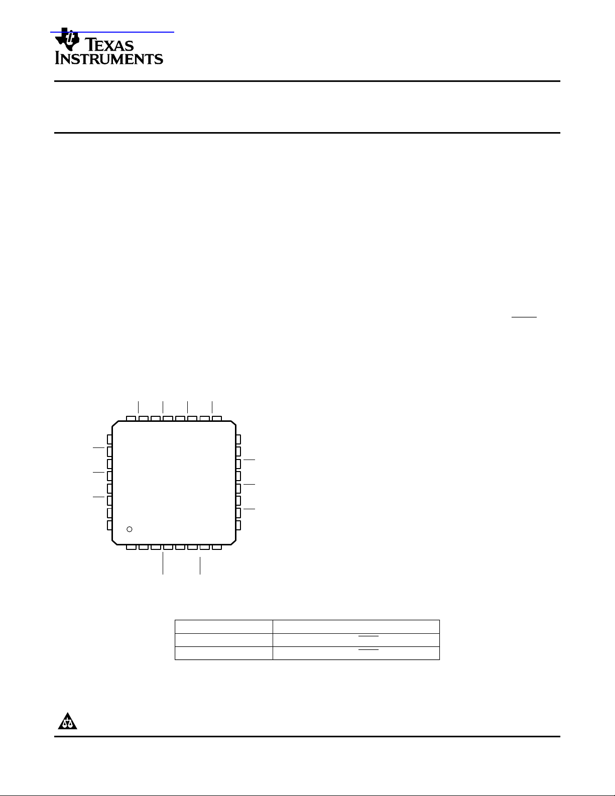
LQFP PACKAGE
(TOP VIEW)
23 22 21 20 19
1 2
25
26
27
28
29
30
31
32
16
15
14
13
12
11
10
9
V
CC
Q7
Q7
Q8
Q8
Q9
Q9
V
CC
V
CC
Q2
Q2
Q1
Q1
Q0
Q0
V
CC
24 18
3 4 5 6 7 8
17
V
CC
CLK_SEL
CLK0
CLK0
V
BB
CLK1
CLK
1
V
EE
Q3Q3Q4Q4Q5Q5Q6
Q6
查询CDCLVP110供应商
LOW-VOLTAGE 1:10 LVPECL/HSTL
WITH SELECTABLE INPUT CLOCK DRIVER
FEATURES DESCRIPTION
• Distributes One Differential Clock Input Pair
LVPECL/HSTL to 10 Differential LVPECL
Clock Outputs
• Fully Compatible With LVECL/LVPECL/HSTL
• Single Supply Voltage Required, ±3.3-V or
±2.5-V Supply
• Selectable Clock Input Through CLK_SEL
• Low-Output Skew (Typ 15 ps) for
Clock-Distribution Applications
• VBB Reference Voltage Output for
Single-Ended Clocking
• Available in a 32-Pin LQFP Package
• Frequency Range From DC to 3.5 GHz
• Pin-to-Pin Compatible With MC100 Series
EP111, ES6111, LVEP111, PTN1111
CDCLVP110
SCAS683A – JUNE 2002 – REVISED AUGUST 2002
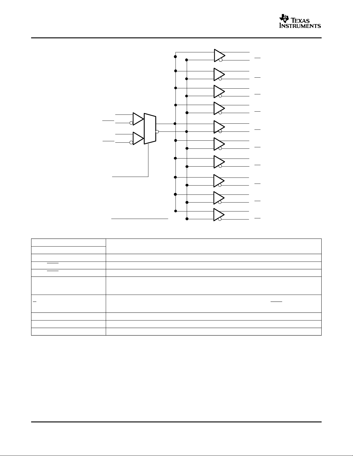
The CDCLVP110 clock driver distributes one
differential clock pair of either LVPECL or HSTL
(selectable) input, (CLK0, CLK1) to ten pairs of
differential LVPECL clock (Q0, Q9) outputs with
minimum skew for clock distribution. The
CDCLVP110 can accept two clock sources into an
input multiplexer. The CLK0 input accepts either
LVECL/LVPECL input signals, while CLK1 accepts an
HSTL input signal when operated under LVPECL
conditions. The CDCLVP110 is specifically designed
for driving 50-Ω transmission lines.
The VBB reference voltage output is used if
single-ended input operation is required. In this case
the VBB pin should be connected to CLK0 and
bypassed to GND via a 10-nF capacitor.
However, for high-speed performance up to 3.5 GHz,
the differential mode is strongly recommended.
The CDCLVP110 is characterized for operation from
-40°C to 85°C.
PRODUCTION DATA information is current as of publication date.
Products conform to specifications per the terms of the Texas
Instruments standard warranty. Production processing does not
necessarily include testing of all parameters.
Please be aware that an important notice concerning availability, standard warranty, and use in critical applications of Texas
Instruments semiconductor products and disclaimers thereto appears at the end of this data sheet.
FUNCTION TABLE
CLK_SEL ACTIVE CLOCK INPUT
0 CLK0, CLK0
1 CLK1, CLK1
Copyright © 2002, Texas Instruments Incorporated
Page 2
www.ti.com
CLK_SEL
VBB
30
31
29
28
27
26
23
22
24
21
20
19
18
17
15
14
13
12
11
10
5
CLK0
CLK0
CLK1
CLK1
0
1
3
4
6
7
2
Q0
Q1
Q2
Q3
Q4
Q5
Q6
Q7
Q8
Q9
Q0
Q1
Q2
Q3
Q4
Q5
Q7
Q6
Q9
Q8
CDCLVP110
SCAS683A – JUNE 2002 – REVISED AUGUST 2002
TERMINAL FUNCTIONS
TERMINAL
NAME NO.
CLK_SEL 2 Clock select. Used to select between CLK0 and CLK1 input pairs.
CLK0, CLK0 3, 4 Differential LVECL/LVPECL input pair
CLK1, CLK1 6, 7 Differential HSTL input pair
Q [9:0] 20, 22, 24, 27, LVECL/LVPECL clock outputs, these outputs provide low-skew copies of CLKn.
11, 13, 15, 18,
29, 31
10, 12, 14, 17,
Q[9:0] 19, 21,23, 26, LVECL/LVPECL complementary clock outputs, these outputs provide copies of CLKn.
28, 30
V
BB
V
CC
V
EE
5 Reference voltage output for single-ended input operation
1, 9, 16, 25, 32 Supply voltage
8 Device ground or negative supply voltage in ECL mode
2
DESCRIPTION
Page 3
www.ti.com
CDCLVP110
SCAS683A – JUNE 2002 – REVISED AUGUST 2002
ABSOLUTE MAXIMUM RATINGS
V
CC
V
I
V
O
I
IN
V
EE
I
BB
I
O
T
stg
(1) Stresses beyond those listed under "absolute maximum ratings” may cause permanent damage to the device. These are stress ratings
only, and functional operation of the device at these or any other conditions beyond those indicated under "recommended operating
conditions” is not implied. Exposure to absolute-maximum-rated conditions for extended periods may affect device reliability.
Supply voltage -0.3 V to 4.6 V
Input voltage -0.3 V to V
Output voltage -0.3 V to V
Input current ±20 mA
Negative supply voltage -0.3 V to 4.6 V
Sink/source current -1 to 1 mA
DC output current -50 mA
Storage temperature range -65°C to 150°C
RECOMMENDED OPERATING CONDITIONS
V
CC
(1)
T
A
(1) Operating junction temperature affects device lifetime. The continuous operation junction temperature is recommended to be at max
110°C. The device ac and dc parameters are specified up to 85°C ambient temperature. See the PCB Layout Guidelines for
CDCLVP110 application note, literature number SCAA057 for more details.
Supply voltage (relative to VEE) 2.375 2.5/3.3 3.8 V
Operating free-air temperature -40 85 °C
(1)
+ 0.5 V
CC
+ 0.5 V
CC
MIN NOM MAX UNIT
PACKAGE THERMAL IMPEDANCE
Θ
Thermal resistance junction to ambient
JA
Θ
Thermal resistance junction to case 51 °C/W
JC
(1) According to JESD 51-7 standard.
LVECL DC ELECTRICAL CHARACTERISTICS
Vsupply: V
I
EE
I
CC
I
IN
V
BB
V
IH
= 0 V, V
CC
PARAMETER TEST CONDITIONS MIN TYP MAX UNIT
Supply internal current Absolute value of current 25°C 45 82 mA
Output and internal supply
current
Input current Includes pullup/pulldown resistors 25°C, 150 µA
Internally generated bias
voltage
High-level input voltage
(CLK_SEL)
= -2.375 V to -3.8 V
EE
TEST CONDITION MIN MAX UNIT
0 LFM 78 °C/W
(1)
150 LFM 73 °C/W
250 LFM 71 °C/W
500 LFM 68 °C/W
-40°C 40 78
85°C 48 85
-40°C 343
All outputs terminated 50 Ω to V
- 2 V 25°C 370 mA
CC
85°C 380
-40°C,
85°C
-40°C -1.38 -1.26
For V
= -3 to -3.8 V, IBB= -0.2 mA 25°C -1.42 -1.26
EE
85°C -1.45 -1.26
-40°C,
V
= -2.375 to -2.75 V, IBB= -0.2 mA 25°C, -1.38 -1.16
EE
85°C
-40°C,
25°C, -1.165 -0.88 V
85°C
V
3
Page 4

www.ti.com
CDCLVP110
SCAS683A – JUNE 2002 – REVISED AUGUST 2002
LVECL DC ELECTRICAL CHARACTERISTICS (continued)
Vsupply: V
V
IL
VIN
PP
V
CM
V
OH
V
OL
V
OD
(1) VIN
CC
= 0 V, V
= -2.375 V to -3.8 V
EE
PARAMETER TEST CONDITIONS MIN TYP MAX UNIT
Low-level input voltage
(CLK_SEL)
Input amplitude (CLK0, CLK0) Difference of input 9 VIH-V
Common-mode voltage (CLK0,
CLK0)
Cross point of input 9 average (V
High-level output voltage IOH= -21 mA 25°C -1.2 -0.9 V
Low-level output voltage IOL= -5 mA 25°C -1.85 -1.45 V
Differential output voltage swing 25°C, 600 V
minimum and maximum is required to maintain ac specifications, actual device function tolerates a minimum VIN
PP
Terminated with 50 Ω to V
Figure 3
-40°C,
25°C, -1.81 -1.475 V
85°C
-40°C,
, See Note
IL
(1)
25°C, 0.5 1.3 V
85°C
-40°C,
, VIL) 25°C, V
IH
85°C
+ 1 -0.3 V
EE
-40°C -1.26 -0.9
85°C -1.15 -0.9
-40°C -1.85 -1.5
85°C -1.85 -1.4
- 2 V, See
CC
-40°C,
85°C
of 100 mV.
PP
LVPECL/HSTL DC ELECTRICAL CHARACTERISTICS
Vsupply: V
I
EE
I
CC
I
IN
V
BB
V
IH
V
IL
VIN
PP
V
IC
= 2.375 V to 3.8 V, V
CC
PARAMETER TEST CONDITIONS MIN TYP MAX UNIT
Supply internal current Absolute value of current 25°C 45 82 mA
Output and internal
supply current
Input current Includes pullup/pulldown resistors 25°C, 150 µA
Internally generated
bias voltage
High-level input voltage
(CLK_SEL)
Low-level input voltage
(CLK_SEL)
Input amplitude (CLK0,
CLK0)
Common-mode
voltage (CLK0, CLK0)
= 0 V
EE
-40°C 40 78
85C 48 85
-40°C 343
All outputs terminated 50 Ω to V
- 2 V 25°C 370 mA
CC
85°C 380
-40°C,
85°C
-40°C V
V
= -3 to -3.8 V, IBB= -0.2 mA 25°C V
EE
85°C V
-40°C,
V
= -2.375 to -2.75 V, IBB= -0.2 mA 25°C, V
EE
85°C
-40°C, 25°C, 85°C V
-40°C, 25°C, 85°C V
-40°C,
Difference of input 9 VIH-V
, see Note
IL
(1)
25°C, 0.5 1.3 V
85°C
-40°C,
Cross point of input 9 average (V
, VIL) 25°C, 1 V
IH
85°C
- 1.38 V
CC
- 1.42 V
CC
- 1.45 V
CC
- 1.38 V
CC
- 1.165 V
CC
- 1.81 V
CC
- 1.26
CC
- 1.26
CC
- 1.26
CC
- 1.16
CC
- 0.88 V
CC
- 1.475 V
CC
CC
V
- 0.3 V
(1) VIN
minimum and maximum is required to maintain ac specifications, actual device function tolerates a minimum VIN
PP
of 100 mV.
PP
4
Page 5

www.ti.com
LVPECL/HSTL DC ELECTRICAL CHARACTERISTICS (continued)
Vsupply: V
V
ID
V
I(x)
V
OH
V
OL
V
OD
= 2.375 V to 3.8 V, V
CC
= 0 V
EE
PARAMETER TEST CONDITIONS MIN TYP MAX UNIT
Differential input
voltage (CLK1, CLK1)
Input crossover
voltage (CLK1, CLK1)
High-level output
voltage
Low-level output
voltage
Difference of input VIH-V
Cross point of input 9 average (V
IOH= -21 mA 25°C V
IOL= -5 mA 25°C V
Differential output Terminated with 50 Ω to V
voltage swing Figure 4
AC ELECTRICAL CHARACTERISTICS
Vsupply: V
t
pd
t
sk(pp)
t
sk(o)
t
(JITTER)
f
(max)
tr/t
f
= 2.375 V to 3.8 V, V
CC
= 0 V or LVECL/LVPECL input V
EE
PARAMETER TEST CONDITIONS MIN TYP MAX UNIT
Differential propagation delay CLK0,
CLK0 to all Q0, Q0… Q9, Q9
Input condition: VCM = 1 V, -40°C, 230 350
V
PP
Part-to-part skew See Note B and Figure 1 25°C, 70 ps
Output-to-output skew See Note A and Figure 1 25°C, 15 30 ps
Cycle-to-cycle RMS jitter 25°C, < 1 ps
Functional up to 3.5 GHz, timing -40°C,
Maximum frequency specifications apply at 1 GHz, 25°C, 3500 MHz
see Figure 3 85°C
Output rise and fall time (20%, 80%) 25°C, 100 200 ps
CDCLVP110
SCAS683A – JUNE 2002 – REVISED AUGUST 2002
, See Note
IL
CC
(1)
, VIL) 25°C, 0.68 0.9 V
IH
- 2 V, See
= 0.5 V 25°C, ps
-40°C,
25°C, 0.4 1.9 V
85°C
-40°C,
85°C
-40°C V
85°C V
-40°C V
85°C V
- 1.26 V
CC
- 1.2 V
CC
- 1.15 V
CC
- 1.85 V
CC
- 1.85 V
CC
- 1.85 V
CC
CC
-40°C,
25°C, 600 mV
85°C
CC
= 0 V, V
= -2.375 V to -3.8 V
EE
85°C
-40°C,
85°C
-40°C,
85°C
-40°C,
85°C
-40°C,
85°C
- 0.9
CC
- 0.9 V
CC
- 0.9
CC
- 1.5
CC
- 1.45 V
- 1.4
CC
HSTL INPUT
Vsupply: V
t
pd
t
sk(pp)
t
sk(o)
t
(JITTER)
= 2.375 V to 3.8 V, V
CC
= 0 V
EE
PARAMETER TEST CONDITIONS MIN TYP MAX UNIT
Differential propagation delay CLK0, Input condition: Vx= 0.68 V,
CLK0 to all Q0, Q0… Q9, Q9 V
= 0.4 V
dif
-40°C,
25°C, 290 370 ps
85°C
-40°C,
Part-to-part skew See Note B and Figure 1 25°C, 70 ps
85°C
-40°C,
Output to output skew See Note A and Figure 1 25°C, 10 30 ps
85°C
-40°C,
Cycle-to-cycle RMS jitter 25°C, <1 ps
85°C
5
Page 6

www.ti.com
o
o
o
o
o
CLKn
Q0
Q1
Q2
Q9
CLKn
Q0
Q1
Q2
Q9
t
PLH2
t
PLH2
t
PLH1
t
PLH1
t
PLH0
t
PLH0
t
PLH9
t
PLH9
CDCLVP110
SCAS683A – JUNE 2002 – REVISED AUGUST 2002
HSTL INPUT (continued)
Vsupply: V
f
(max)
tr/t
f
= 2.375 V to 3.8 V, V
CC
PARAMETER TEST CONDITIONS MIN TYP MAX UNIT
Maximum frequency specifications apply at 1 GHz, See 25°C, 3500 MHz
Output rise and fall time (20%, 80%) 25°C, 100 200 ps
= 0 V
EE
Functional up to 3.5 GHz, timing -40°C,
Figure 4 85°C
-40°C,
85°C
A. Output skew is calculated as the greater of: The difference between the fastest and the slowest t
the difference between the fastest and the slowest t
(n = 0, 1,...9).
PHLn
B. Part-to-part skew, is calculated as the greater of: The difference between the fastest and the slowest t
1,...9) across multiple devices or the difference between the fastest and the slowest t
multiple devices.
Figure 1. Waveform for Calculating Both Output and Part-to-Part Skew
6
PHLn
(n = 0, 1,...9) or
PLHn
(n = 0, 1,...9) across
(n = 0,
PLHn
Page 7

www.ti.com
CDCLVP110
Driver
LVPECL
Receiver
ZO = 50 Ω
ZO = 50 Ω
V
EE
V
CC
VT = VCC - 2 V
50 Ω
50 Ω
Yn
Yn
0
100
200
300
400
500
600
700
800
900
1 1.5 2 2.5 3 3.5
VCC = 2.375 V
TA = -40°C to 85°C
f - Frequency - GHz
DIFFERENTIAL OUTPUT VOLTAGE SWING
vs
FREQUENCY
V
OUT(PP)min
- Differential Output Voltage Swing - mV
CDCLVP110
SCAS683A – JUNE 2002 – REVISED AUGUST 2002
Figure 2. Typical Termination for Output Driver (See the Interfacing Between LVPECL, LVDS, and CML
Application Note, Literature Number SCAA056)
Figure 3. LVPECL Input Using CLK0 Pair, VCM = 1 V, VIN
= 0.5 V
dif
7
Page 8

www.ti.com
0
100
200
300
400
500
600
700
800
900
1000
1 1.5 2 2.5 3 3.5
VCC = 2.375 V
TA = -40°C to 85°C
f - Frequency - GHz
DIFFERENTIAL OUTPUT VOLTAGE SWING
vs
FREQUENCY
V
OUT(PP)min
- Differential Output Voltage Swing - mV
CDCLVP110
SCAS683A – JUNE 2002 – REVISED AUGUST 2002
8
Figure 4. HSTL Input Using CLK1 Pair, VCM = 0.68 V, VIN
= 0.4 V
dif
Page 9

PACKAGE OPTION ADDENDUM
www.ti.com
4-Mar-2005
PACKAGING INFORMATION
Orderable Device Status
(1)
Package
Type
Package
Drawing
Pins Package
Qty
Eco Plan
CDCLVP110VF ACTIVE LQFP VF 32 250 None CU NIPDAU Level-2-220C-1 YEAR
CDCLVP110VFR ACTIVE LQFP VF 32 1000 None CU NIPDAU Level-2-220C-1 YEAR
(1)
The marketing status values aredefined as follows:
ACTIVE: Product device recommended for new designs.
LIFEBUY: TI has announced that the device will be discontinued, and a lifetime-buy period is in effect.
NRND: Not recommended for new designs. Device is in production to support existing customers, but TI does not recommend using this part in
a new design.
PREVIEW: Device has been announced but is not in production. Samples may or may not be available.
OBSOLETE: TI has discontinued the production of the device.
(2)
Eco Plan - May not be currently available - please check http://www.ti.com/productcontent for the latest availability information and additional
product content details.
None: Not yet available Lead (Pb-Free).
Pb-Free (RoHS): TI's terms "Lead-Free" or "Pb-Free" mean semiconductor products that are compatible with the current RoHS requirements
for all 6 substances, including the requirement that lead not exceed 0.1% by weight in homogeneous materials. Where designed to be soldered
at high temperatures, TI Pb-Free products are suitable for use in specified lead-free processes.
Green (RoHS & no Sb/Br): TI defines "Green" to mean "Pb-Free" and in addition, uses package materials that do not contain halogens,
including bromine (Br) or antimony (Sb) above 0.1% of total product weight.
(3)
MSL, Peak Temp. -- The Moisture Sensitivity Level rating according to the JEDECindustry standard classifications, and peak solder
temperature.
(2)
Lead/Ball Finish MSL Peak Temp
(3)
Important Information and Disclaimer:The information provided on this page represents TI's knowledge and belief as of the date that it is
provided. TI bases its knowledge and belief on information provided by third parties, and makes no representation or warranty as to the
accuracy of such information. Efforts are underway to better integrate information from third parties. TI has taken and continues to take
reasonable steps to provide representative and accurate information but may not have conducted destructive testing or chemical analysis on
incoming materials and chemicals. TI and TI suppliers consider certain information to be proprietary, and thus CAS numbers and other limited
information may not be available for release.
In no event shall TI's liability arising out of such information exceed the total purchase price of the TI part(s) at issue in this document sold by TI
to Customer on an annual basis.
Addendum-Page 1
Page 10

MECHANICAL DATA
MTQF002B – JANUARY 1995 – REVISED MAY 2000
VF (S-PQFP-G32) PLASTIC QUAD FLATPACK
25
32
1,45
1,35
0,80
24
0,45
0,25
17
1
5,60 TYP
7,20
SQ
6,80
9,20
SQ
8,80
8
16
9
0,20
M
0,05 MIN
Seating Plane
0,13 NOM
Gage Plane
0,25
0°–7°
0,75
0,45
1,60 MAX
NOTES: A. All linear dimensions are in millimeters.
B. This drawing is subject to change without notice.
POST OFFICE BOX 655303 • DALLAS, TEXAS 75265
0,10
4040172/D 04/00
1
Page 11

IMPORTANT NOTICE
Texas Instruments Incorporated and its subsidiaries (TI) reserve the right to make corrections, modifications,
enhancements, improvements, and other changes to its products and services at any time and to discontinue
any product or service without notice. Customers should obtain the latest relevant information before placing
orders and should verify that such information is current and complete. All products are sold subject to TI’s terms
and conditions of sale supplied at the time of order acknowledgment.
TI warrants performance of its hardware products to the specifications applicable at the time of sale in
accordance with TI’s standard warranty. Testing and other quality control techniques are used to the extent TI
deems necessary to support this warranty . Except where mandated by government requirements, testing of all
parameters of each product is not necessarily performed.
TI assumes no liability for applications assistance or customer product design. Customers are responsible for
their products and applications using TI components. To minimize the risks associated with customer products
and applications, customers should provide adequate design and operating safeguards.
TI does not warrant or represent that any license, either express or implied, is granted under any TI patent right,
copyright, mask work right, or other TI intellectual property right relating to any combination, machine, or process
in which TI products or services are used. Information published by TI regarding third-party products or services
does not constitute a license from TI to use such products or services or a warranty or endorsement thereof.
Use of such information may require a license from a third party under the patents or other intellectual property
of the third party, or a license from TI under the patents or other intellectual property of TI.
Reproduction of information in TI data books or data sheets is permissible only if reproduction is without
alteration and is accompanied by all associated warranties, conditions, limitations, and notices. Reproduction
of this information with alteration is an unfair and deceptive business practice. TI is not responsible or liable for
such altered documentation.
Resale of TI products or services with statements different from or beyond the parameters stated by TI for that
product or service voids all express and any implied warranties for the associated TI product or service and
is an unfair and deceptive business practice. TI is not responsible or liable for any such statements.
Following are URLs where you can obtain information on other Texas Instruments products and application
solutions:
Products Applications
Amplifiers amplifier.ti.com Audio www.ti.com/audio
Data Converters dataconverter.ti.com Automotive www.ti.com/automotive
DSP dsp.ti.com Broadband www.ti.com/broadband
Interface interface.ti.com Digital Control www.ti.com/digitalcontrol
Logic logic.ti.com Military www.ti.com/military
Power Mgmt power.ti.com Optical Networking www.ti.com/opticalnetwork
Microcontrollers microcontroller.ti.com Security www.ti.com/security
Telephony www.ti.com/telephony
Video & Imaging www.ti.com/video
Wireless www.ti.com/wireless
Mailing Address: Texas Instruments
Post Office Box 655303 Dallas, Texas 75265
Copyright 2005, Texas Instruments Incorporated
 Loading...