

Page 1
查询CDCLVD110供应商
CDCLVD110
PROGRAMMABLE LOW-VOLTAGE 1:10 LVDS CLOCK DRIVER
SCAS684 – SEPTEMBER 2002
D Low-Output Skew <30 ps (Typical) for
Clock-Distribution applications
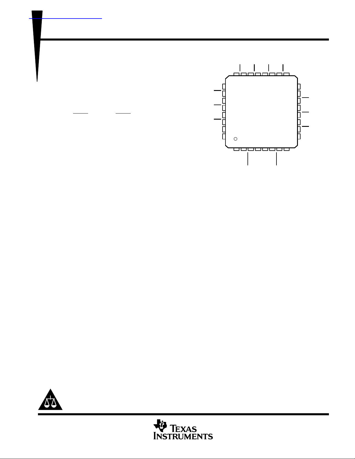
TQFP PACKAGE
(TOP VIEW)
D Distributes One Differential Clock Input to
10 LVDS Differential Clock Outputs
D V
range 2.5 V ±5%
CC
D Typical Signaling Rate Capability of Up to
1.1 GHz
D Configurable Register (SI/CK) Individually
Enables Disables Outputs, Selectable
CLK0, CLK0
or CLK1, CLK1 Inputs
D Full Rail-to-Rail Common-Mode Input
Range
D Receiver Input Threshold ±100 mV
VSS
Q2
Q2
Q1
Q1
Q0
Q0
VDD
Q3Q3Q4Q4Q5Q5Q6
24 18
23 22 21 20 19
25
26
27
28
29
30
31
32
345
12
Q6
17
16
15
14
13
12
11
10
9
67 8
D Available in 32-Pin TQFP Package
SI
D Fail-Safe I/O-Pins for V
Down)
= 0 V (Power
DD
CK
description
The CDCL VD1 10 clock driver distributes one pair of dif ferential L VDS clock inputs (either CLK0 or CLK1) to 10
pairs of differential clock outputs (Q0, Q9) with minimum skew for clock distribution. The CDCLVD110 is
specifically designed for driving 50-Ω transmission lines.
When the control enable is high (EN = 1), the 10 differential outputs are programmable in that each output can
be individually enabled/disabled (3-stated) according to the first 10 bits loaded into the shift register. Once the
shift register is loaded, the last bit selects either CLK0 or CLK1 as the clock input. However, when EN = 0, the
outputs are not programmable and all outputs are enabled.
CLK0
CLK0
V
BB
CLK1
CLK1
EN
VDD
Q7
Q7
Q8
Q8
Q9
Q9
VSS
The CDCLVD110 is characterized for operation from –40 °C to 85°C.
Please be aware that an important notice concerning availability, standard warranty, and use in critical applications of
Texas Instruments semiconductor products and disclaimers thereto appears at the end of this data sheet.
PRODUCTION DATA information is current as of publication date.
Products conform to specifications per the terms of Texas Instruments
standard warranty. Production processing does not necessarily include
testing of all parameters.
POST OFFICE BOX 655303 • DALLAS, TEXAS 75265
Copyright 2002, Texas Instruments Incorporated
1
Page 2
CDCLVD110
PROGRAMMABLE LOW-VOLTAGE 1:10 LVDS CLOCK DRIVER
SCAS684 – SEPTEMBER 2002
functional block diagram
CK
CLK0
CLK0
CLK1
CLK1
SI
EN
0
CLK_SEL
Mux
0
Mux
1
11-Bit Shift Register
11-Bit Control Register
10
1
0198765432
12-Bit
Counter
Q9
Q9
Q8
Q8
Q7
Q7
Q6
Q6
Q5
Q5
Q4
Q4
Q3
Q3
Q2
Q2
Q1
Q1
Q0
V
BB
Q0
2
POST OFFICE BOX 655303 • DALLAS, TEXAS 75265
Page 3
CDCLVD110
PROGRAMMABLE LOW-VOLTAGE 1:10 LVDS CLOCK DRIVER
SCAS684 – SEPTEMBER 2002
Terminal Functions
TERMINAL
NAME NO.
CK 1 I Control register input clock, features a 120-kΩ pullup resistor
SI 2 I Control register serial input/CLK Select, features a 120-kΩ pulldown resistor
CLK0 3 I Complementary differential input, LVDS
CLK0 4 I True differential input, LVDS
V
BB
CLK1 6 I Complementary differential input, LVDS
CLK1 7 I True differential input, LVDS
EN 8 I Control enable (for programmability), features a 120-kΩ pulldown resistor, input
V
SS
V
DD
Q [9:0] 11, 13, 15, 18, 20,
Q[9:0] 10, 12, 14, 17, 19,
5 O Reference voltage output
9, 25 Device ground
16, 32 Supply voltage
22, 24, 27, 29, 31
21,23, 26, 28, 30
absolute maximum ratings
Supply voltage, V
Input voltage, V
Output voltage, V
Driver short circuit current, Qn, Qn
DD
–0.2 V to (VDD + 0.2). . . . . . . . . . . . . . . . . . . . . . . . . . . . . . . . . . . . . . . . . . . . . . . . . . . . . . . . . . . .
I
O
I/O
O Clock outputs, these outputs provide low-skew copies of CLKIN
O Complementary clock outputs, these outputs provide low-skew copies of CLKIN
†
–0.3 V to 2.8 V. . . . . . . . . . . . . . . . . . . . . . . . . . . . . . . . . . . . . . . . . . . . . . . . . . . . . . . . . . . . . .
–0.2 V to (VDD + 0.2). . . . . . . . . . . . . . . . . . . . . . . . . . . . . . . . . . . . . . . . . . . . . . . . . . . . . . . . . .
, I
Continuous. . . . . . . . . . . . . . . . . . . . . . . . . . . . . . . . . . . . . . . . . . . . . . . .
OSD
DESCRIPTION
Electrostatic discharge (HBM 1.5 kΩ, 100 pF), ESD >2000 V. . . . . . . . . . . . . . . . . . . . . . . . . . . . . . . . . . . . . . . .
†
Stresses beyond those listed under “absolute maximum ratings” may cause permanent damage to the device. These are stress ratings only, and
functional operation of the device at these or any other conditions beyond those indicated under “recommended operating conditions” is not
implied. Exposure to absolute-maximum-rated conditions for extended periods may affect device reliability.
recommended operating conditions
Supply voltage, V
Receiver common-mode input voltage, V
Operating free-air temperature, T
DD
IC
A
MIN NOM MAX UNIT
2.375 2.5 2.625 V
0.5|VID| VDD – 0.5|VID| V
–40 85 °C
POST OFFICE BOX 655303 • DALLAS, TEXAS 75265
3
Page 4

CDCLVD110
Su ly current
mA
PROGRAMMABLE LOW-VOLTAGE 1:10 LVDS CLOCK DRIVER
SCAS684 – SEPTEMBER 2002
driver electrical characteristics over recommended operating free-air temperature range (unless
otherwise noted)
PARAMETER TEST CONDITIONS MIN TYP MAX UNIT
|VOD|
∆V
V
OS
∆V
I
OS
V
BB
C
O
receiver electrical characteristics over recommended operating free-air temperature range
(unless otherwise noted)
V
IDH
V
IDL
|VID| Input differential voltage 200 mV
I
IH
I
IL
C
I
Differential output voltage RL = 100 Ω 250 450 600 mV
VOD magnitude change 50 mV
OD
Offset voltage –40°C to 85°C 0.95 1.2 1.45 V
V
magnitude change 350 mV
OS
OS
Output short circuit current
Reference output voltage VDD = 2.5 V, IBB = –100 µA 1.15 1.25 1.35 V
Output capacitance VO = VDD or GND 3 pF
PARAMETER TEST CONDITIONS MIN TYP MAX UNIT
Input threshold high 100 mV
Input threshold low –100 mV
Input current, CLK0/CLK0, CLK1/CLK1
Input capacitance VI = VDD or GND 3 pF
VO = 0 V –20
|VOD| = 0 V
VI = V
DD
VI = 0 V
–5 5 µA
20
mA
supply current electrical characteristics over recommended operating free-air temperature range
(unless otherwise noted)
PARAMETER TEST CONDITIONS MIN TYP MAX UNIT
I
DD
I
DDZ
Supply current
Full loaded All outputs enabled and loaded, RL = 100 Ω, f = 0 Hz 130
No load Outputs enabled, no output load, f = 0 Hz 35
3-State All outputs 3-state by control logic, f = 0 Hz 35
mA
LVDS—switching characteristics over recommended operating free-air temperature range,
= 2.5 V ±5%
V
DD
t
PLH
t
PHL
t
duty
t
sk(o)
t
sk(p)
t
sk(pp)
t
r
t
f
f
clk
PARAMETER
Propagation delay low-to-high
Propagation delay high-to-low
Duty cycle
Output skew Any Qn, Qn 30 ps
Pulse skew Any Qn, Qn 50 ps
Part-to-part skew Any Qn, Qn 600 ps
Output rise time, 20% to 80%, RL = 100 Ω, CL = 5 pF
Output fall time, 20% to 80%, RL = 100 Ω, CL = 5 pF
Max input frequency
FROM
(INPUT)
CLK0, CLK0
CLK1, CLK1
CLK0, CLK0
CLK1, CLK1
CLK0, CLK0
CLK1, CLK1
CLK0, CLK0
CLK1, CLK1
TO
(OUTPUT)
Qn, Qn 2 3 ns
Qn, Qn 2 3 ns
Qn, Qn 45% 55%
Any Qn, Qn 350 ps
Any Qn, Qn 350 ps
Any Qn, Qn 900 1100 MHz
MIN TYP MAX UNIT
4
POST OFFICE BOX 655303 • DALLAS, TEXAS 75265
Page 5

CDCLVD110
PROGRAMMABLE LOW-VOLTAGE 1:10 LVDS CLOCK DRIVER
SCAS684 – SEPTEMBER 2002
control register characteristics over recommended operating free-air temperature range,
VDD = 2.5 V ±5%
PARAMETER TEST CONDITIONS MIN TYP MAX UNIT
f
MAX
t
su
t
h
t
removal
t
w
V
IH
V
IL
I
IH
I
IL
specification of control register
Maximum frequency of shift register 100 150 MHz
Setup time, clock to SI 2 ns
Hold time, clock to SI 1.5 ns
Removal time, enable to clock 1.5 ns
Clock pulse width, minimum 3 ns
Logic input high VDD = 2.5 V 2 V
Logic input low VDD = 2.5 V 0.8 V
Input current, CK pin
Input current, SI and EN pins
Input current, CK pin
Input current, SI and EN pins
VI = V
DD
VI = GND
–5 5
10 30
–10 –30
–5 5
The CDCLVD110 is provided with an 11-bit, serial-in shift register and an 11-bit control register. The control
Register enables/disables each output clock and selects either CLK0 or CLK1 as the input clock. The
CDCLVD110 has two modes of operation:
µA
µA
Programmable Mode (EN=1)
The shift register utilizes a serial input (SI) and a clock input (CK). Once the shift register is loaded with 1 1
clock pulses, the twelfth clock pulse loads the control register. The first bit (bit 0) on SI enables the Q9, Q9
output pair, and the tenth bit (bit 9) enables the Q0, Q0 pair. The eleventh bit (bit 10) on SI selects either
CLK0 or CLK1 as the input clock; a bit value of 0 selects CLK0, whereas a bit value of 1 selects CLK1. To
restart the control register configuration, a reset of the state machine must be done with a clock pulse on CK
(shift register clock input) and EN set to low. The control register can be configured only once after each
reset.
Standard Mode (EN=0)
In this mode, the CDCL VD110 is not programmable and all the clock outputs are enabled. The clock input
(CLK0 or CLK1) is selected with the SI pin, as is shown in the table entitled control register.
state-machine inputs
EN SI CK OUTPUT
L L X All outputs enabled, CLK0 selected, control register disabled, default state
L H X All outputs enabled, CLK1 selected, control register disabled
H L ↑ First stage stores L, other stage stores data of previous stage
H H First stage stores H, other stage stores data of previous stage
L X Reset of state machine, shift and control registers
control register
BIT 10 BITS [0–9] QN[0–9]
L H CLK0
H H CLK1
X L Outputs disabled
POST OFFICE BOX 655303 • DALLAS, TEXAS 75265
5
Page 6

CDCLVD110
PROGRAMMABLE LOW-VOLTAGE 1:10 LVDS CLOCK DRIVER
SCAS684 – SEPTEMBER 2002
serial input (SI) sequence
BIT 10 BIT 9 BIT 8 BIT 7 BIT 6 BIT 5 BIT 4 BIT 3 BIT 2 BIT 1 BIT 0
CLK_SEL Q0 Q1 Q2 Q3 Q4 Q5 Q6 Q7 Q8 Q9
truth table for control logic
CK EN SI CLK0 CLK0 CLK1 CLK1 Q (0–9) Q(0–9)
L L L L H X X L H
L L L H L X X H L
L L L Open Open X X L H
L L H X X L H L H
L L H X X H L H L
L L H X X Open Open L H
All outputs enabled X = Don’t care
APPLICATION INFORMATION
Fail-Safe information:
For V
fail-safe biasing at input pins can be accomplished with a 10-kΩ pullup resistor from CLK0/CLK1 to VDD and
a 10-kΩ pulldown resistor from CLK0
= 0 V (power-down mode) the CDCLVD110 has fail-safe input and output pins. In power-on mode,
DD
/CLK1 to GND.
LVDS Receiver Input termination:
The L VDS receiver inputs need to have 100-Ω termination resistors placed as close as possible across the input
pins.
Control Inputs termination:
No external termination is required. The CK control input has an internal 120-kΩ pullup resistor while SI– and
EN– control inputs each have an internal 120-kΩ pulldown resistor. If the control pins are left open per the
default, all outputs are enabled, CLK0, CLK0
is selected, and the control register is disabled.
6
POST OFFICE BOX 655303 • DALLAS, TEXAS 75265
Page 7

CLKIN
CLKIN
Q0
Q0
CDCLVD110
PROGRAMMABLE LOW-VOLTAGE 1:10 LVDS CLOCK DRIVER
SCAS684 – SEPTEMBER 2002
PARAMETER MEASUREMENT INFORMATION
NOTES: A. Output skew, t
– The difference between the fastest and the slowest t
– The difference between the fastest and the slowest t
B. Part–to–part skew, t
– The difference between the fastest and the slowest t
– The difference between the fastest and the slowest t
C. Pulse skew, t
(t
) propagation delays when a single switching input causes one or more outputs to switch, t
PLH
is sometimes referred to as pulse width distortion or duty cycle skew.
t
PLH1
Q1
Q1
t
PLH2
Q2
Q2
t
PLH3
Q3
Q3
t
PLH4
Q9
Q9
t
PLH9
Figure 1. Waveforms for Calculation of t
, is calculated as the greater of:
sk(o)
, is calculated as the greater of:
sk(pp)
, is calculated as the magnitude of the absolute time difference between the high-to-low (t
sk(p)
(n = 1, 2,…10)
PLHn
(n = 1, 2,…10)
PHLn
(n = 1, 2,…10) across multiple devices
PLHn
(n = 1, 2,…10) across multiple devices
PHLn
t
PHL1
t
PHL2
t
PHL3
t
PHL4
t
PHL9
sk(o)
and t
sk(pp)
sk(p)
= | t
) and the low-to-high
PHL
– t
PHL
|. Pulse skew
PLH
POST OFFICE BOX 655303 • DALLAS, TEXAS 75265
7
Page 8

CDCLVD110
PROGRAMMABLE LOW-VOLTAGE 1:10 LVDS CLOCK DRIVER
SCAS684 – SEPTEMBER 2002
PARAMETER MEASUREMENT INFORMATION
Differential Output Signal
VOD = (Qn) – (Qn)
80%
–250 mV
–5%
Figure 2. Test Criteria for f
5%
20%
t/2t/2
, Duty Cycle, tr, tf, V
clk
250 mV
0-V
Differential
OD
8
POST OFFICE BOX 655303 • DALLAS, TEXAS 75265
Page 9

CDCLVD110
PROGRAMMABLE LOW-VOLTAGE 1:10 LVDS CLOCK DRIVER
SCAS684 – SEPTEMBER 2002
MECHANICAL DATA
VF (S-PQFP-G32) PLASTIC QUAD FLATPACK
25
32
1,45
1,35
0,80
24
0,45
0,25
17
1
5,60 TYP
7,20
SQ
6,80
9,20
SQ
8,80
8
16
9
0,20
M
0,05 MIN
Seating Plane
0,13 NOM
Gage Plane
0,25
0°–ā7°
0,75
0,45
1,60 MAX
NOTES: A. All linear dimensions are in millimeters.
B. This drawing is subject to change without notice.
POST OFFICE BOX 655303 • DALLAS, TEXAS 75265
0,10
4040172/D 04/00
9
Page 10

IMPORTANT NOTICE
Texas Instruments Incorporated and its subsidiaries (TI) reserve the right to make corrections, modifications,
enhancements, improvements, and other changes to its products and services at any time and to discontinue
any product or service without notice. Customers should obtain the latest relevant information before placing
orders and should verify that such information is current and complete. All products are sold subject to TI’s terms
and conditions of sale supplied at the time of order acknowledgment.
TI warrants performance of its hardware products to the specifications applicable at the time of sale in
accordance with TI’s standard warranty . Testing and other quality control techniques are used to the extent TI
deems necessary to support this warranty . Except where mandated by government requirements, testing of all
parameters of each product is not necessarily performed.
TI assumes no liability for applications assistance or customer product design. Customers are responsible for
their products and applications using TI components. T o minimize the risks associated with customer products
and applications, customers should provide adequate design and operating safeguards.
TI does not warrant or represent that any license, either express or implied, is granted under any TI patent right,
copyright, mask work right, or other TI intellectual property right relating to any combination, machine, or process
in which TI products or services are used. Information published by TI regarding third–party products or services
does not constitute a license from TI to use such products or services or a warranty or endorsement thereof.
Use of such information may require a license from a third party under the patents or other intellectual property
of the third party , or a license from TI under the patents or other intellectual property of TI.
Reproduction of information in TI data books or data sheets is permissible only if reproduction is without
alteration and is accompanied by all associated warranties, conditions, limitations, and notices. Reproduction
of this information with alteration is an unfair and deceptive business practice. TI is not responsible or liable for
such altered documentation.
Resale of TI products or services with statements different from or beyond the parameters stated by TI for that
product or service voids all express and any implied warranties for the associated TI product or service and
is an unfair and deceptive business practice. TI is not responsible or liable for any such statements.
Mailing Address:
Texas Instruments
Post Office Box 655303
Dallas, Texas 75265
Copyright 2002, Texas Instruments Incorporated
 Loading...