

Page 1
www.DataSheet4U.com
www.ti.com
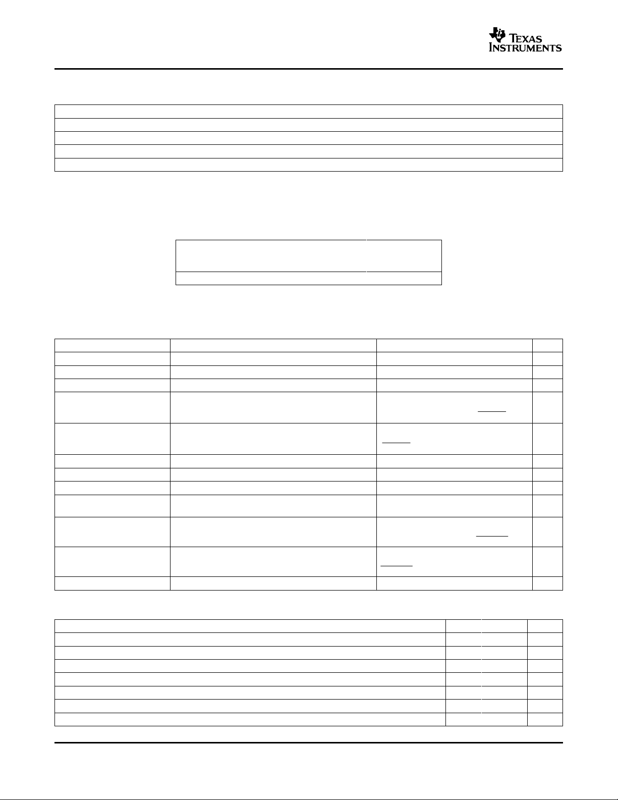
1
2
3
4
5
6
7
8
9
10
11
12
24
23
22
21
20
19
18
17
16
15
14
13
VDDREF
REFCLK
VDDP
GNDP
GND
LEADLAG
DLYCTRL
GNDPA
VDDPA
VDDPD
STOPB
PWRDNB
P0
P1
VDDO
GNDO
CLKOUT
NC
CLKOUTB
GNDO
VDDO
MULT0
MULT1
P2
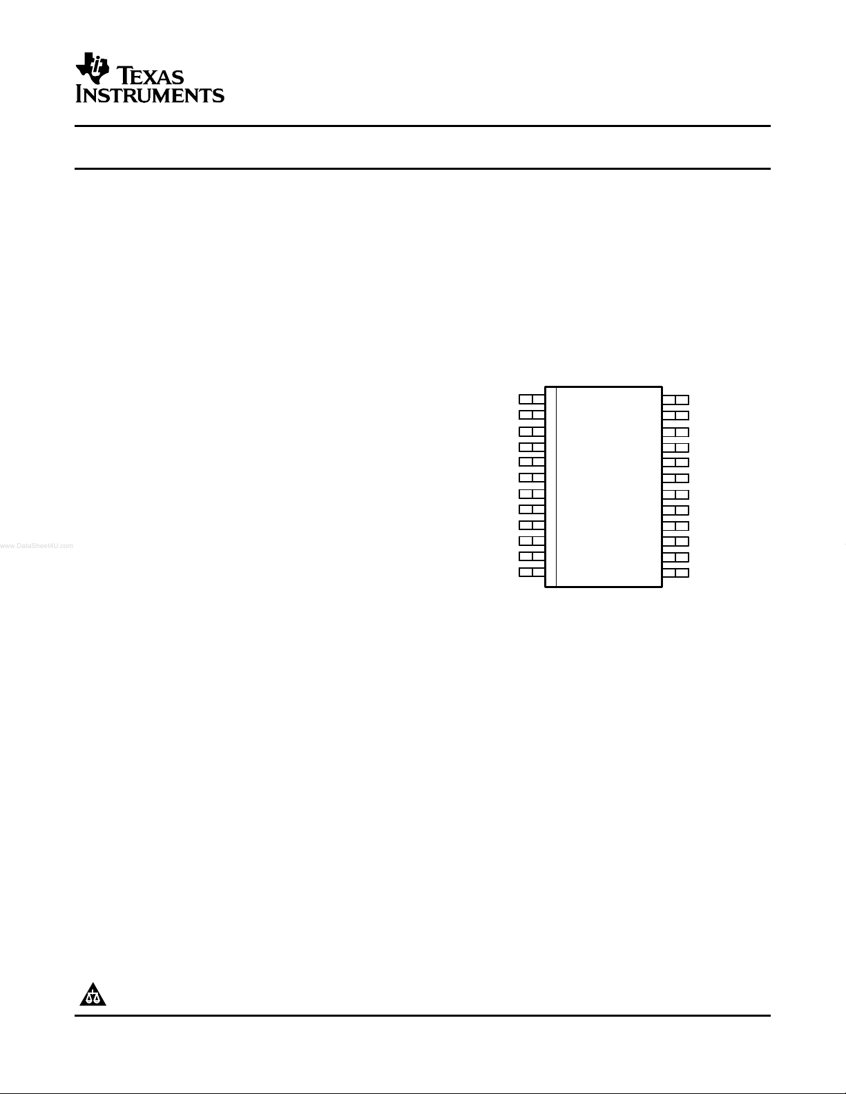
DBQ PACKAGE
(TOP VIEW)
CLOCK MULTIPLIER WITH DELAY CONTROL AND PHASE ALIGNMENT
CDCF5801A
SCAS816 – MARCH 2006
FEATURES
• Low-Jitter Clock Multiplier: ×1, ×2, ×4, ×8
• Fail-Safe Power Up Initialization
• Programmable Bidirectional Delay Steps of
1.3 mUI
• Output Frequency Range of 25 MHz to
280 MHz
• Input Frequency Range of 12.5 MHz to
240 MHz
• Low Jitter Generation
• Single-Ended REFCLK Input With Adjustable
Trigger Level (Works With LVTTL, HSTL, and
LVPECL)
• Differential/Single-Ended Output
• Output Can Drive LVPECL, LVDS, and LVTTL
• Three Power Operating Modes to Minimize
Power
• Low Power Consumption (< 190 mW at
280 MHz/3.3 V)
• Packaged in a Shrink Small-Outline Package
(DBQ)
• No External Components Required for PLL
• Spread Spectrum Clock Tracking Ability to
Reduce EMI (SSC)
APPLICATIONS
• Video Graphics
• Gaming Products
• Datacom
• Telecom
• Noise Cancellation Created by FPGAs
DESCRIPTION
The CDCF5801A provides clock multiplication from a reference clock (REFCLK) signal with the unique capability
to delay or advance the CLKOUT/CLKOUTB with steps of only 1.3 mUI through a phase aligner. For every rising
edge on the DLYCTRL pin the CLKOUT is delayed by a 1.3-mUI step size as long as the LEADLAG input
detects a low signal at the time of the DLYCTRL rising edge. Similarly for every rising edge on the DLYCTRL pin
the CLKOUT is advanced by a 1.3-mUI step size as long as the LEADLAG pin is high during the transition. This
unique capability allows the device to phase align (zero delay) between CLKOUT/CLKOUTB and any one other
CLK in the system by feeding the clocks that need to be aligned to the DLYCTRL and the LEADLAG pins. Also it
provides the capability to program a fixed delay by providing the proper number of edges on the DLYCTRL pin,
while strapping the LEADLAG pin to dc high or low. Further possible applications are:
• Aligning the rising edge of the output clock signal to the input clock rising edge
• Avoiding PLL instability in applications that require very long PLL feedback lines
• Isolation of jitter and digital switching noise
• Limitation of jitter in systems with good ppm frequency stability
The CDCF5801A has a fail-safe power up initialization state-machine which supports proper operation under all
power up conditions.
PRODUCTION DATA information is current as of publication date.
Products conform to specifications per the terms of the Texas
Instruments standard warranty. Production processing does not
necessarily include testing of all parameters.
Please be aware that an important notice concerning availability, standard warranty, and use in critical applications of Texas
Instruments semiconductor products and disclaimers thereto appears at the end of this data sheet.
Copyright © 2006, Texas Instruments Incorporated
Page 2

www.ti.com
CDCF5801A
SCAS816 – MARCH 2006
The CDCF5801A provides clock multiplication and division from a reference clock (REFCLK) signal. The device
is optimized to have extremely low jitter impact from input to output. The predivider pins MULT[0:1] and
post-divider pins P[0:2] provide selection for frequency multiplication and division ratios, generating
CLKOUT/CLOUTKB frequencies ranging from 25 MHz to 280 MHz with clock input references (REFCLK) ranging
from 12.5 MHz to 240 MHz. See Table 1 for detailed frequency support. The selection of pins MULT[0:1] and
P[1:2] determines the multiplication value of 1, 2, 4, or 8. The CDCF5801A offers several power-down/
high-impedance modes, selectable by pins P0, STOPB and PWRDN. Another unique capability of the
CDCF5801A is the high sensitivity and wide common-mode range of the clock-input pin REFCLK by varying the
voltage on the VDDREF pin. The clock signal outputs CLKOUT and CLKOUTB can be used independently to
generate single-ended clock signals. The CLKOUT/CLKOUTB outputs can also be combined to generate a
differential output signal suitable for LVDS, LVPECL, or HSTL/SSTL signaling. The CDCF5801A is characterized
for operation over free-air temperatures of -40°C to 85°C.
2
Submit Documentation Feedback
Page 3
www.ti.com
PWRDNB
>CLK
01 div2
00 div4
11 div8
10 div16
2
PLL
VDDREF/2
12.5-240 MHz
Control
P0
VDDP
GNDP
MULT[0:1]
Delay
Phase Aligner
DLY+ DLY-
VDDPD/2
DLYCTRL
0-240 MHz
LEADLAG
0-280 MHz
CLKOUTB
CLKOUT
25-280 MHz
div2
div4
div8
11
10
01
2
P[1:2]
GNDO
STOPB
VDDO
GNDPA
VDDPA
CDCF5801A
SCAS816 – MARCH 2006
FUNCTIONAL BLOCK DIAGRAM
Submit Documentation Feedback
3
Page 4
www.ti.com
CDCF5801A
SCAS816 – MARCH 2006
TERMINAL FUNCTIONS
TERMINAL
NAME NO.
CLKOUT 2018 O Output CLK signal (low-noise CMOS) Complementary output CLK signal (low-noise CMOS)
CLKOUTB
DLYCTRL 7 I Every rising edge on this pin delays/advances the CLKOUT/CLKOUTB signal by 1/768
GND 5 GND for VDDREF and VDDPD
GNDO 17, 21 GND for the output pins (CLKOUT, CLKOUTB)
GNDP 4 GND for the PLL
GNDPA 8 GND for phase aligner, digital logic, and inputs P[0:2], MULT[0:1], STOPB, PWRDNB
LEADLAG 6 I Controls whether the output CLK is delayed or advanced relative to REFCLK. See Table 3 .
MULT0 15 I PLL multiplication factor select. See Table 1 .
MULT1
NC 19 Not connected; leave pin floating or tied to GND.
P0 24 I Mode control pins (see Table 1 )
P1 23 I Post divider control (see Table 1 )
P2 13 P[1:2] = 01: div8
PWRDNB 12 I Active-low power-down state. CLKOUT/CLKOUTB goes low, See Table 2 ).
REFCLK 2 I Reference input clock
STOPB 11 I Active low output disabler, PLL and PA still running, CLKOUT and CLKOUTB goes to a dc value as
VDDO 16, 22 VDD for the output pin (CLKOUT, CLKOUTB) and power down circuit
VDDP 3 VDD for PLL and input buffer
VDDPA 9 VDD for phase aligner, digital logic, and inputs P[0:2], MULT[0:1], and STOPB
VDDPD 10 Reference voltage for inputs LEADLAG and DLYCTRL
VDDREF 1 Reference voltage for REFCLK
14 MULT[0:1] = 10: ×16
I/O DESCRIPTION
CLKOUT/CLKOUTB period (1.3 mUI). (E.g., for a 90-degree delay or advancement one needs to
provide 192 rising edges). See Table 3 .
MULT[0:1] = 11: ×8
MULT[0:1] = 00: ×4
MULT[0:1] = 01: ×2
0 - Normal operation
1 - High-Z outputs and other special settings
P[1:2] = 11: div2
P[1:2] = 10: div4
0 - IC in power down
1 - Normal operation
listed in Table 2 .
0 - Outputs disabled
1 - Normal operation
th
of the
4
Submit Documentation Feedback
Page 5
www.ti.com
CDCF5801A
SCAS816 – MARCH 2006
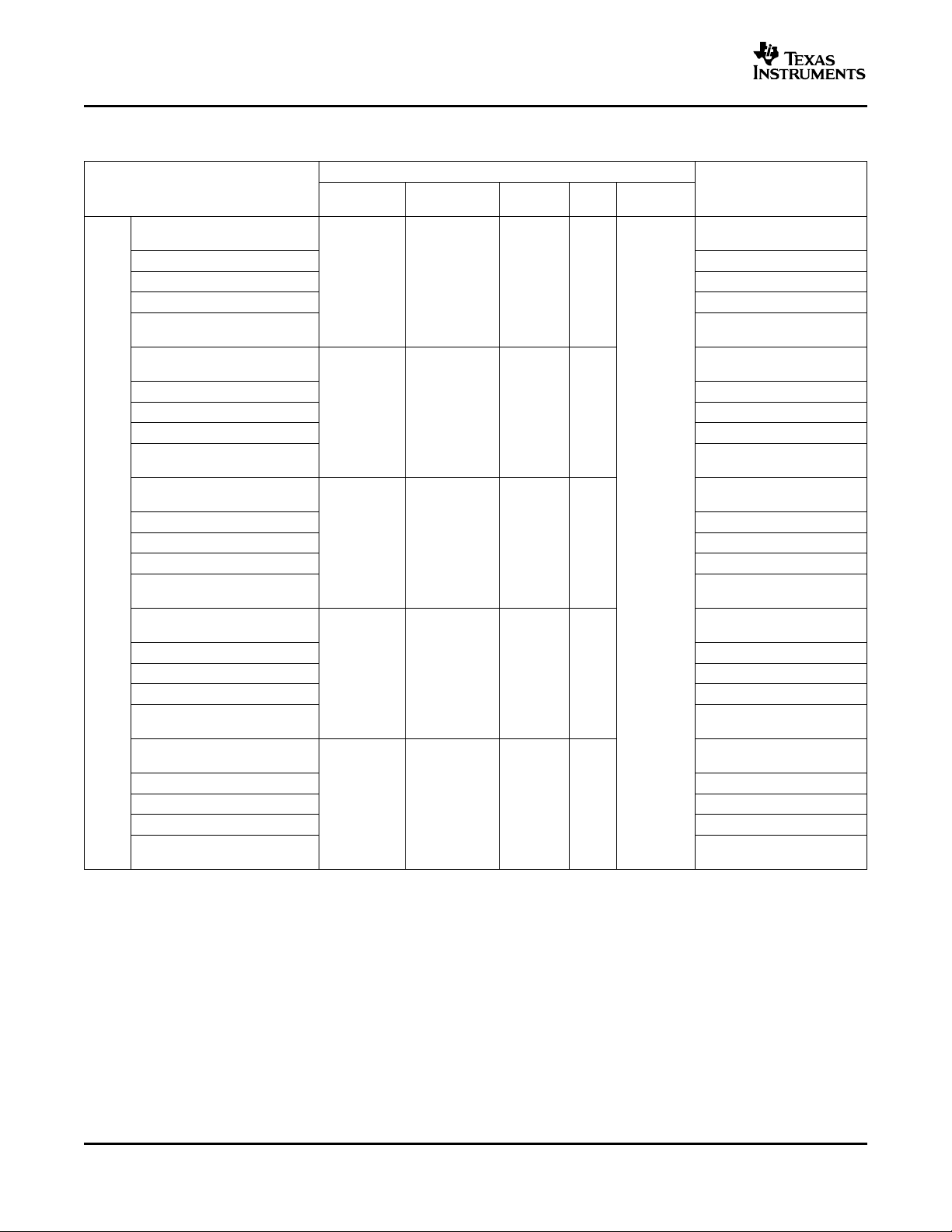
Table 1. Input-to-Output Settings
INPUT-TO-OUTPUT
MULTIPLICATION-RATIO
8 12.5 35 100 280 1 0 1 1
4
2 25 78 50 156 1 1 0 1 0 Normal operation
1 50 156 50 156 0 0 1 0
INPUT OUTPUT
FREQUENCY (MHz) FREQUENCY (MHz)
FROM TO FROM TO MULT0 MULT1 P0 P1 P2
12.5 39 50 156 1 0 1 0
25 70 100 280 1 1 1 1
12.5 39 25 78 1 0 0 1
50 140 100 280 0 0 1 1
25 78 25 78 1 1 0 1
100 240 100 240 0 1 1 1
CLKOUT high-impedance
CLOUOTB high-impedance
CLKOUT = high
CLKOUTB = high
CLKOUT = P2
CLKOUTB = P2
(1) There is some overlapping of the input frequency ranges for multiplication ratios of 1, 2, and 4. For example, an input frequency of 30
MHz for a multiplication ratio of four falls within both the 12.5 to 39-MHz range and the 25 to 70-MHz range. For best device operation in
a case such as this, always select the input frequency range nearer to the top of the table.
PREDIVIDER POST DIVIDER
X X 0 0
X X 1 0 1 Special mode of operation
X X 1 X
NOTE
(1)
PLL DIVIDER/MULITPLIER SELECTION
Table 2. Power Down Modes
STATE PWRDNB STOPB CLKOUT and CLKOUTB
Power down 0 X GNDO
Clock stop 1 0 VO, STOP
Normal 1 1 See Table 1
Table 3. Programmable Delay and Phase Alignment
DLYCTR NOTE LEADLAG CLKOUT and CLKOUTB
Each rising step size: 1/768 of the CLKOUT period (1.3 mUI) at P[1:2] = 11
edge+ 1/1536 of the CLKOUT period (0.65 mUI) at P[1:2] = 10
Each rising step size: 1/768 of the CLKOUT period (1.3 mUI) at P[1:2] = 11
edge+ 1/1536 of the CLKOUT period (0.65 mUI) at P[1:2] = 10
For every 32 edges, there are one or two
edges for which the phase aligner does not
update the phase. Therefore, CLKOUT
phase is not updated for every 32
nd
The frequency of the DLYCTRL pin should
always be equal to or less than the
frequency of the LEADLAG pin.
HI
edge.
LO
Advanced by one step:
1/3072 of the CLKOUT period (0.325 mUI) at P[1:2] = 01
Delayed by one step:
1/3072 of the CLKOUT period (0.325 mUI) at P[1:2] = 01
Submit Documentation Feedback
5
Page 6
www.ti.com
VDDPD
2
0.2
VDDPD
2
0.2
VDDREF
2
0.2
VDDREF
2
0.2
CDCF5801A
SCAS816 – MARCH 2006
ABSOLUTE MAXIMUM RATINGS
over operating free-air temperature (unless otherwise noted)
(2)
V
DDx
Supply voltage range -0.5 V to 4 V
Voltage range at any output terminal -0.5 V to V
Voltage range at any input terminal -0.5 V to V
T
stg
Storage temperature range -65°C to 150°C
Lead temperature 1,6 mm (1/16 inch) from case for 10 seconds 260°C
(1) Stresses beyond those listed under, , absolute maximum ratings” may cause permanent damage to the device. These are stress ratings
only, and functional operation of the device at these or any other conditions beyond those indicated under, , recommended operating
conditions” is not implied. Exposure to absolute-maximum-rated conditions for extended periods may affect device reliability.
(2) All voltage values are with respect to the GND terminals.
POWER DISSIPATION RATING TABLE
PACKA
DBQ 830 mW 8.3 mW/°C 332 mW
(1) This is the inverse of the junction-to-ambient thermal resistance
TA≤ 25°C POWER DERATING TA= 85°C
GE
RATING FACTOR
when board-mounted and with no air flow.
RECOMMENDED OPERATING CONDITIONS
VDDP, VDDPA, VDDO Supply voltage 3 3.3 3.6 V
V
IH (CMOS)
V
IL (CMOS)
High-level input voltage 0.7 VDD V
Low-level input voltage 0.3 VDD V
(1)
(1)
ABOVE TA= 25°C
+ 0.5 V
DD
+ 0.5 V
DD
POWER RATING
MIN NOM MAX UNIT
VIL(DLYCTRL, LEADLAG) Input signal low voltage V
VIH(DLYCTRL, LEADLAG) Input signal high voltage V
(VDDPD) Input reference voltage for DLYCNTRL and LEADLAG 1.2 VDD V
I
OH
I
OL
(VDDREF) (see Application
section)
High-level output current -16 mA
Low-level output current 16 mA
Input reference voltage for REFCLK 1.2 VDD V
VIL(see Application section) REFCLK input low voltage V
VIH(see Application section) REFCLK input high voltage V
T
A
Operating free-air temperature -40 85 °C
TIMING REQUIREMENTS
PARAMETER MIN MAX UNIT
F
SR Input slew rate 1 4 V/ns
Input frequency of modulation, (if driven by SSC CLKIN) 33 kHz
mod
Modulation index, nonlinear maximum 0.5% 0.6%
Input duty cycle on REFCLK 40% 60%
Input frequency on REFCLK 12.5 240 MHz
Output frequency on CLKOUT and CLKOUTB 25 280 MHz
Allowable frequency on DLYCTRL 240 MHz
6
Submit Documentation Feedback
Page 7

www.ti.com
VDDO
2
0.2
VDDO
2
0.2
TIMING REQUIREMENTS (continued)
PARAMETER MIN MAX UNIT
Allowable frequency on LEADLAG 280 MHz
Allowable duty cycle on DLYCTRL and LEADLAG pins 25% 75%
ELECTRICAL CHARACTERISTICS
over recommended operating conditions (unless otherwise noted)
PARAMETER TEST CONDITIONS
V
O(STOP)
Output voltage during Clkstop mode See Figure 1 1.1 2 V
CDCF5801A
SCAS816 – MARCH 2006
(1)
MIN TYP
(2)
MAX UNIT
V
O(X)
V
O
V
IK
V
OH
V
OL
I
OH
I
OL
I
OZ
I
OZ(STOP)
I
OZ(PD)
I
IH
I
IL
Output crossing-point voltage See Figure 1 and Figure 4 V
Output voltage swing (V
Input clamp voltage V
High-level output voltage V
Low-level output voltage V
High-level output current V
Low-level output current V
- VOL) See Figure 1 1.7 2.9 V
OH
= 3 V, II= -18 mA -1.2 V
DD
V
= 3 to 3.6 V, See Figure 1 2 2.5
DD
V
= 3 V, IOH= -16 mA 2.2
DD
V
= 3 to 3.6 V, See Figure 1 0.4 0.6
DD
V
= 3 V, IOH= 16 mA 0.5
DD
V
= 3.135 V, VO= 1 V -32 -52
DD
= 3.3 V, VO= 1.65 V -51 mA
DD
V
= 3.465 V, VO= 3.135 V -14.5 -21
DD
V
= 3.135 V, VO= 1.95 V 43 61.5
DD
= 3.3 V, VO= 1.65 V 65 mA
DD
V
= 3.465 V, VO= 0.4 V 25.5 40
DD
High-impedance-state output current P0 = 1, P1 = P2 = 0 ±10 µA
High-impedance-state output current
during Clk Stop
High-impedance-state output current
in power-down state
REFCLK; STOPB; V
High-level PWRDNB; P[0:2];
input current MULT[0:1];
DLYCTRL; LEADLAG
Stop = 0, VO= GND or V
PWRDNB = 0, VO= GND or V
= 3.6 V, VI= V
DD
V
= 3.6 V, VI=0 -10 µA
DD
DD
DD
DD
-10 100 µA
±100 µA
Output High state RIat IO-14.5 mA to -16.5 mA 15 35 50
Z
O
I
REF
C
I
C
O
IDD(PD) Supply current in power-down state 4 mA
impedance
(single
ended)
Reference
current
Input capacitance VI= V
Low state RIat IO14.5 mA to 16.5 mA 10 17 35
VDDREF; VDDPD V
= 3.6 V
DD
or GND 2 pF
DD
Output capacitance VO= GND or V
REFCLK = 0 MHz to 280 MHz;
PWRDNB = 0; STOPB = 1
PWRDNB = 0 50 µA
PWRDNB = 1 0.5 mA
DD
3 pF
IDD(CLKSTOP) Supply current in CLK stop state BUSCLK configured for 280 MHz 44 mA
IDD(NORMAL) 75 mA
(1) V
DD
(2) All typical values are at V
Supply current (normal operation BUSCLK 280 MHz, MULT[0:1] = 10;
mode) P[0:2] = 011; Load , See Figure 1
refers to any of the following; VDDP, VDDREF, VDDO, VDDPD, and VDDPA
= 3.3 V, TA= 25°C.
DD
10 µA
Ω
Submit Documentation Feedback
7
Page 8
www.ti.com
CDCF5801A
SCAS816 – MARCH 2006
JITTER SPECIFICATION
over recommended free-air temperature range and V
PARAMETER TYP (ps) MAX (ps)
Period rms (1-sigma jitter, full 25 25 11 001 20 48
frequency band)
Period p-p 120 225
Cycle to cycle + 70 165
Cycle to cycle - 70 165
RMS phase jitter (accumulated, 80 160
100 kHz-12.5 MHz)
Period rms (1-sigma jitter, full 50 50 11 001 7 15
frequency band)
Period p-p 37 75
Cycle to cycle + 27 55
Cycle to cycle - 27 55
RMS phase jitter (accumulated, 27 65
100 kHz-25 MHz)
Period rms (1-sigma jitter, full 100 100 00 010 5 14
frequency band)
Period p-p 30 65
t
Cycle to cycle + tight to 24 55
(jitter)
Cycle to cycle - 24 55
RMS phase jitter (accumulated, 35 65
100 kHz-40 MHz)
Period rms (1-sigma jitter, full 156 156 00 010 4 8
frequency band)
Period p-p 20 40
Cycle to cycle + 17 40
Cycle to cycle - 17 40
RMS phase jitter (accumulated, 15 35
100 kHz-40 MHz)
Period rms (1-sigma jitter, full 200 200 01 011 8 15
frequency band)
Period p-p 38 60
Cycle to cycle + 5 55
Cycle to cycle - 35 55
RMS phase jitter (accumulated, 30 60
100 kHz-40 MHz)
REFCLK CLKOUT
(MHz) (MHz)
range (unless otherwise noted)
CC
TEST CONDITIONS
MULT[0:1] P[0:2] NOTES
Phase
aligner
running
(CLKOUT
tight to
LEADLAG;
REFCLK
DLYCTRL).
All typical
values are
at
VDD = 3.3
V,
TA= 25°C.
8
Submit Documentation Feedback
Page 9

www.ti.com
JITTER SPECIFICATION (continued)
over recommended free-air temperature range and V
PARAMETER TYP (ps) MAX (ps)
Period rms (1-sigma jitter, full 25 200 10 011 4 11
frequency band)
Period p-p 20 48
Cycle to cycle + 16 45
Cycle to cycle - 16 45
Period rms (1-sigma jitter, full 25 100 10 010 4 11
frequency band)
Period p-p 22 55
Cycle to cycle + 15 45
Cycle to cycle - 15 45
Period rms (1-sigma jitter, full 70 280 11 011 4 11
frequency band)
Period p-p 18 48
Cycle to cycle + 15 45
t
Cycle to cycle - 15 45
(jitter)
Period rms (1-sigma jitter, full 25 50 10 001 6 16
frequency band)
Period p-p 34 75
Cycle to cycle + 20 65
Cycle to cycle - 20 65
Period rms (1-sigma jitter, full 78 156 11 010 3 11
frequency band)
Period p-p 15 44
Cycle to cycle + 13 40
Cycle to cycle - 13 40
Period rms (1-sigma jitter, full 62.5 125 00 011 6 20
frequency band)
Period p-p 35 80
Cycle to cycle + 25 75
Cycle to cycle - 25 75
REFCLK CLKOUT
(MHz) (MHz)
range (unless otherwise noted)
CC
TEST CONDITIONS
CDCF5801A
SCAS816 – MARCH 2006
MULT[0:1] P[0:2] NOTES
Phase
aligner
not running
(LEADLAG
= 0,
DLYCTRL =
0). All
typical
values are
at
VDD = 3.3
V, TA=
25°C.
SWITCHING CHARACTERISTICS
over recommended operating free-air temperature range (unless otherwise noted)
PARAMETER TEST CONDITIONS MIN TYP MAX UNIT
t
(DC)
tr, t
Output duty cycle over 1000 cycles See Figure 3 42% 58%
Output rise and fall times (measured at 20%-80% of output voltage See Figure 5 150 250 350 ps
f
STATE TRANSITION LATENCY SPECIFICATIONS
PARAMETER FROM TO MIN TYP MAX UNIT
Delay time, PWRDNB ↑ to CLKOUT /
t
(powerup)
CLKOUTB settled
Delay time, PWRDNB ↑ to internal PLL
and clock are on and settled
Power down Normal See Figure 6 ms
Submit Documentation Feedback
TEST
CONDITION
3
3
9
Page 10

www.ti.com
CLKOUT
10 pF
50 Ω
50 Ω
CLKOUTB
V
CM
CLKOUT
CLKOUTB
t
CYCLE
(i)
Cycle-to-Cycle Jitter (t
(jitter)
) = | t
CYCLE
(i) - t
CYCLE
(i+1) | over 1000 consecutive cycles
t
CYCLE
(i+1)
CDCF5801A
SCAS816 – MARCH 2006
STATE TRANSITION LATENCY SPECIFICATIONS (continued)
PARAMETER FROM TO MIN TYP MAX UNIT
Delay time, power up to CLKOUT
t
(VDDpowerup)
t
(MULT)
t
(CLKON)
t
(CLKSETL)
t
(CLKOFF)
t
(powerdown)
t
(STOP)
t
(ON)
output settled
Delay time, power up to internal PLL
and clock are on and settled
MULT0 and MULT1 change to
CLKOUT output resettled
STOPB ↑ to CLKOUT glitch-free clock
edges
STOPB ↑ to CLKOUT output settled to
within 50 ps of the phase before CLK stop Normal See Figure 8 20 cycles
STOPB was disabled
STOPB ↓ to CLKOUT output disabled Normal CLK stop See Figure 8 5 ns
Delay time, PWRDNB ↓ to the device in
the power-down mode
Maximum time in CLKSTOP (STOPB =
0) before reentering normal mode STOPB Normal See Figure 8 100 µs
(STOPB = 1)
Minimum time in normal mode (STOPB
= 1) before reentering CLKSTOP Normal CLK stop See Figure 8 100 ms
(STOPB = 0)
TEST
CONDITION
3
V
DD
Normal See Figure 6 ms
3
Normal Normal See Figure 7 1 ms
CLK stop Normal See Figure 8 10 ns
Normal Power down See Figure 6 1 ms
PARAMETER MEASUREMENT INFORMATION
TESTING CONDITIONS
Figure 1. Test Load and Voltage Definitions V
, V
OH
, V
OL
O(STOP)
10
Figure 2. Cycle-to-Cycle Jitter
Submit Documentation Feedback
Page 11

www.ti.com
CLKOUT
CLKOUTB
t
PW+
t
CYCLE
Duty Cycle = (t
PW+/tCYCLE
)
CLKOUT
CLKOUTB
V
O(X)+
V
O(X), nom
V
O(X)-
80%
t
f
t
r
20%
V
OL
V
OH
PWRDNB
CLKOUTB
t
(powerdown)
t
(powerup)
CLKOUT
MULT0
and/or
MULT1
CLKOUTB
t
(MULT)
CLKOUT
PARAMETER MEASUREMENT INFORMATION (continued)
Figure 3. Output Duty Cycle
Figure 4. Crossing Point Voltage
CDCF5801A
SCAS816 – MARCH 2006
Figure 5. Voltage Waveforms
Figure 6. PWRDNB Transition Timings
Figure 7. MULT Transition Timings
Submit Documentation Feedback
11
Page 12

www.ti.com
STOPB
t
(CLKOFF)
(see Note A)
t
(ON)
t
(STOP)
t
(CLKSETL)
t
(CLKON)
(see Note A)
Clock output settled
within 50 ps of the
phase before disabled
Clock enabled
and glitch free
Output clock
not specified
glitches ok
CLKOUT
CLKOUTB
CDCF5801A
SCAS816 – MARCH 2006
PARAMETER MEASUREMENT INFORMATION (continued)
A. V
ref
= VO±200 mV
Figure 8. STOPB Transition Timings
12
Submit Documentation Feedback
Page 13

www.ti.com
Z = 50 Ω
Z = 50 Ω
CDCV304
Clock Buffer
25 MHz
P0
P1
VDDO
GNDO
CLKOUT
NC
CLKOUTB
GNDO
VDDO
MULT0
MULT1
P2
VDDREF
REFCLK
VDDP
GNDP
GND
LEADLAG
DLYCTRL
GNDPA
VDDPA
VDDPD
STOPB
PWRDNB
3.3 V
CLK
35 Ω
3.3 V
3.3 V
CDCF5801A
CDCV304
Clock Buffer
CLK
Z = 50 Ω; Length = L1
25 MHz
25 MHz
25 MHz
Z = 50 Ω
Outputs are Phase Aligned
Between the Two Buffers
3.3 V
Z = 50 Ω; Length = L1
30 Ω
3.3 V
CDCF5801A
SCAS816 – MARCH 2006
APPLICATION INFORMATION
APPLICATION EXAMPLE
The following figure shows an example of using the CDCF5801A as a phase aligner de-skewing the unknown
buffer delay of the two CDCV304s in the circuit. This circuitry would not be possible with a simple PLL because
the feedback of the PLL would have the second CDCV304 in the loop, causing instability of the PLL due to a
long delay.
Figure 9. Application Example
NOTE:
If an active element (microcontroller, ASIC, DSP< FPYA, DSP, etc.) is used in the
CDCF5801A CLKOUT to DLYCTRL feedback loop, see application report SCAA075.
SELECTING VDDREF
Generally, VDDREF can be set to any value between 1.2 V and VDD. The setting of VDDREF directly influences
the trigger voltage of the input. Special care must be taken when using small signal swings to drive the
CVDCF5801 input (e.g., PECL). It is recommended to connect VDDREF directly to VDD, ac-couple the REFCLK
input, and rebias the signal.
The following circuit is recommended to drive the CDCF5801A from a differential clock signal like PECL.
Submit Documentation Feedback
13
Page 14

www.ti.com
Z = 50 Ω
VDDREF
REFCLK
GNDP
GND
CDCF5801A
100 Ω
150 Ω
150 Ω
PECL
3.3 V ± 10%
100 Ω
R1
R2
CDCF5801A
SCAS816 – MARCH 2006
APPLICATION INFORMATION (continued)
A. NOTE: If more signal swing is required and an unterminated transmission is on option, then R1 and R2 can both be
replaced with 10-k Ω resistors.
Figure 10. Driving the CDCF5801A From a Differential Clock Signal
Submit Documentation Feedback
14
Page 15

www.ti.com
Revision History
DATE REV PAGE SECTION DESCRIPTION
15 MAR * – – Original version
05
CDCF5801A
SCAS816 – MARCH 2006
Submit Documentation Feedback
15
Page 16

PACKAGE OPTION ADDENDUM
www.ti.com
6-Dec-2006
PACKAGING INFORMATION
Orderable Device Status
CDCF5801ADBQ ACTIVE SSOP/
CDCF5801ADBQG4 ACTIVE SSOP/
CDCF5801ADBQR ACTIVE SSOP/
CDCF5801ADBQRG4 ACTIVE SSOP/
(1)
The marketing status values are defined as follows:
(1)
Package
Type
QSOP
QSOP
QSOP
QSOP
Package
Drawing
Pins Package
Qty
Eco Plan
DBQ 24 50 Green (RoHS &
no Sb/Br)
DBQ 24 50 Green (RoHS &
no Sb/Br)
DBQ 24 2500 Green (RoHS&
no Sb/Br)
DBQ 24 2500 Green (RoHS&
no Sb/Br)
ACTIVE: Product device recommended for new designs.
LIFEBUY: TI has announced that the device will be discontinued, and a lifetime-buy period isin effect.
NRND: Not recommended for new designs. Device is in production to support existing customers, but TI does not recommend using this part in
a new design.
PREVIEW: Device has been announced but is not in production. Samples may or may notbe available.
OBSOLETE: TI has discontinued the production of the device.
(2)
Eco Plan - The planned eco-friendly classification: Pb-Free (RoHS), Pb-Free (RoHS Exempt), or Green (RoHS & no Sb/Br) - please check
http://www.ti.com/productcontent for the latest availability information and additional product content details.
TBD: The Pb-Free/Green conversion plan has not been defined.
Pb-Free (RoHS): TI's terms "Lead-Free" or "Pb-Free" mean semiconductor products that are compatible with the current RoHS requirements
for all 6 substances, including the requirement that lead not exceed 0.1% by weight in homogeneous materials. Where designed to be soldered
at high temperatures, TI Pb-Free products are suitable for use in specified lead-free processes.
Pb-Free (RoHS Exempt): This component has a RoHS exemption for either 1) lead-based flip-chip solder bumps used between the die and
package, or 2) lead-based die adhesive used between the die and leadframe. The component is otherwise considered Pb-Free (RoHS
compatible) as defined above.
Green (RoHS & no Sb/Br): TI defines "Green" to mean Pb-Free (RoHS compatible), and free of Bromine (Br) and Antimony (Sb) based flame
retardants (Br or Sb do not exceed 0.1% by weight in homogeneous material)
(2)
Lead/Ball Finish MSL Peak Temp
CU NIPDAU Level-2-260C-1 YEAR
CU NIPDAU Level-2-260C-1 YEAR
CU NIPDAU Level-2-260C-1 YEAR
CU NIPDAU Level-2-260C-1 YEAR
(3)
(3)
MSL, Peak Temp. -- The Moisture Sensitivity Level rating according to the JEDEC industry standard classifications, and peak solder
temperature.
Important Information and Disclaimer:The information provided on this page represents TI's knowledge and belief as of the date that it is
provided. TI bases its knowledge and belief on information provided by third parties, and makes no representation or warranty as to the
accuracy of such information. Efforts are underway to better integrate information from third parties. TI has taken and continues to take
reasonable steps to provide representative and accurate information but may not have conducted destructive testing or chemical analysis on
incoming materials and chemicals. TI and TI suppliers consider certain information to be proprietary, and thus CAS numbers and other limited
information may not be available for release.
In no event shall TI's liability arising out of such information exceed the total purchase price of the TI part(s) at issue in this document sold by TI
to Customer on an annual basis.
Addendum-Page 1
Page 17

Page 18

IMPORTANT NOTICE
Texas Instruments Incorporated and its subsidiaries (TI) reserve the right to make corrections, modifications,
enhancements, improvements, and other changes to its products and services at any time and to discontinue
any product or service without notice. Customers should obtain the latest relevant information before placing
orders and should verify that such information is current and complete. All products are sold subject to TI’s terms
and conditions of sale supplied at the time of order acknowledgment.
TI warrants performance of its hardware products to the specifications applicable at the time of sale in
accordance with TI’s standard warranty. Testing and other quality control techniques are used to the extent TI
deems necessary to support this warranty . Except where mandated by government requirements, testing of all
parameters of each product is not necessarily performed.
TI assumes no liability for applications assistance or customer product design. Customers are responsible for
their products and applications using TI components. To minimize the risks associated with customer products
and applications, customers should provide adequate design and operating safeguards.
TI does not warrant or represent that any license, either express or implied, is granted under any TI patent right,
copyright, mask work right, or other TI intellectual property right relating to any combination, machine, or process
in which TI products or services are used. Information published by TI regarding third-party products or services
does not constitute a license from TI to use such products or services or a warranty or endorsement thereof.
Use of such information may require a license from a third party under the patents or other intellectual property
of the third party, or a license from TI under the patents or other intellectual property of TI.
Reproduction of information in TI data books or data sheets is permissible only if reproduction is without
alteration and is accompanied by all associated warranties, conditions, limitations, and notices. Reproduction
of this information with alteration is an unfair and deceptive business practice. TI is not responsible or liable for
such altered documentation.
Resale of TI products or services with statements different from or beyond the parameters stated by TI for that
product or service voids all express and any implied warranties for the associated TI product or service and
is an unfair and deceptive business practice. TI is not responsible or liable for any such statements.
Following are URLs where you can obtain information on other Texas Instruments products and application
solutions:
Products Applications
Amplifiers amplifier.ti.com Audio www.ti.com/audio
Data Converters dataconverter.ti.com Automotive www.ti.com/automotive
DSP dsp.ti.com Broadband www.ti.com/broadband
Interface interface.ti.com Digital Control www.ti.com/digitalcontrol
Logic logic.ti.com Military www.ti.com/military
Power Mgmt power.ti.com Optical Networking www.ti.com/opticalnetwork
Microcontrollers microcontroller.ti.com Security www.ti.com/security
Low Power Wireless www.ti.com/lpw Telephony www.ti.com/telephony
Video & Imaging www.ti.com/video
Wireless www.ti.com/wireless
Mailing Address: Texas Instruments
Post Office Box 655303 Dallas, Texas 75265
Copyright 2006, Texas Instruments Incorporated
 Loading...