


www.ti.com
Y4
Y5
Crystal or
Clock Input
V
DD
GND
Vctr
V
DDOUT
S2/S1/S0or
SDA/SCL
Y1
VCXO
XO
LVCMOS
3
Y2
Y3
LV
CMOS
LV
CMOS
PLL1
withSSC
LV
CMOS
LV
CMOS
LV
CMOS
PLL2
withSSC
Y6
Y7
LV
CMOS
LV
CMOS
PLL3
withSSC
Y8
Y9
LV
CMOS
LV
CMOS
PLL4
withSSC
Xin/Clk 1 24 Xout
S0 2 23 S1/SDA
Vdd 3 22 S2/SCL
Vctr 4 21 Y1
GND 5 20 GND
Vddout 6 19 Y2
Y4 7 18 Y3
Y5 8 17 Vddout
GND 9 16 Y6
Vddout 10 15 Y7
Y8 11 14 GND
Y9 12 13 Vdd
Divider
and
Output
Control
EEPROM
Programming
and
ControlRegister
Programmable 4-PLL VCXO Clock Synthesizer with 1.8V and 3.3V I/Os
CDCE949
CDCEL949
SCAS844 – JUNE 2007
FEATURES
• Member of Programmable Clock Generator
Family
– CDCE949/CDCEL949: 4 PLLs, 9 Outputs
– CDCE937/CDCEL937: 3 PLLs, 7 Outputs
– CDCE925/CDCEL925: 2 PLLs, 5 Outputs
– CDCE913/CDCEL913: 1 PLLs, 3 Outputs
• In-System Programmability and EEPROM
– Serial Programmable Volatile Register
– Non-Volatile EEPROM to Store Customer
Settings
• Very Flexible Input Clocking Concept
– External Crystal: 8 to 32 MHz
– On-Chip VCXO: Pull-Range ± 150 ppm
– Single-Ended LVCMOS up to 160 MHz
• Selectable Output Frequency up to 230 MHz
• Very Low-Noise PLL Core
– Integrated PLL Loop Filter Components
– Very Low Period Jitter (typ 60 ps)
• Highly Flexible Clock Driver
– Three User-Definable Control Inputs
[S0/S1/S2] e.g. SSC-Selection, Frequency
Switching, Output Enable or Power Down
– Programmable SSC Modulation
– Enables 0-PPM Clock Generation
– Generates Common Clock Frequencies
Used with TI DaVinci™, OMAP™, DSPs
– Generates Highly-Accurate Clocks for
Video, Audio, USB, IEEE1394, RFID,
BlueTooth™, WLAN, Ethernet and GPS
• 1.8 V Device Power Supply
• Separate Output Supply Pins
– CDCE949: 3.3 V and 2.5 V
– CDCEL949: 1.8 V
• Wide Temperature Range –40 ° C to 85 ° C
• Packaged in TSSOP
• Development and Programming Kit for Ease
PLL Design and Programming (TI-Pro Clock)
APPLICATIONS
• D-TV, HD-TV, STB, IP-STB, DVD-Player,
DVD-Recorder, Printer
• General Purpose Frequency Synthesizing
Please be aware that an important notice concerning availability, standard warranty, and use in critical applications of Texas
Instruments semiconductor products and disclaimers thereto appears at the end of this data sheet.
DaVinci, OMAP, Pro Clock are trademarks of Texas Instruments.
BlueTooth is a trademark of Bluetooth SIG, Inc.
I2C is a trademark of Philips Electronics.
PRODUCTION DATA information is current as of publication date.
Products conform to specifications per the terms of the Texas
Instruments standard warranty. Production processing does not
necessarily include testing of all parameters.
Copyright © 2007, Texas Instruments Incorporated
www.ti.com
CDCE949
CDCEL949
SCAS844 – JUNE 2007
These devices have limited built-in ESD protection. The leads should be shorted together or the device placed in conductive foam
during storage or handling to prevent electrostatic damage to the MOS gates.
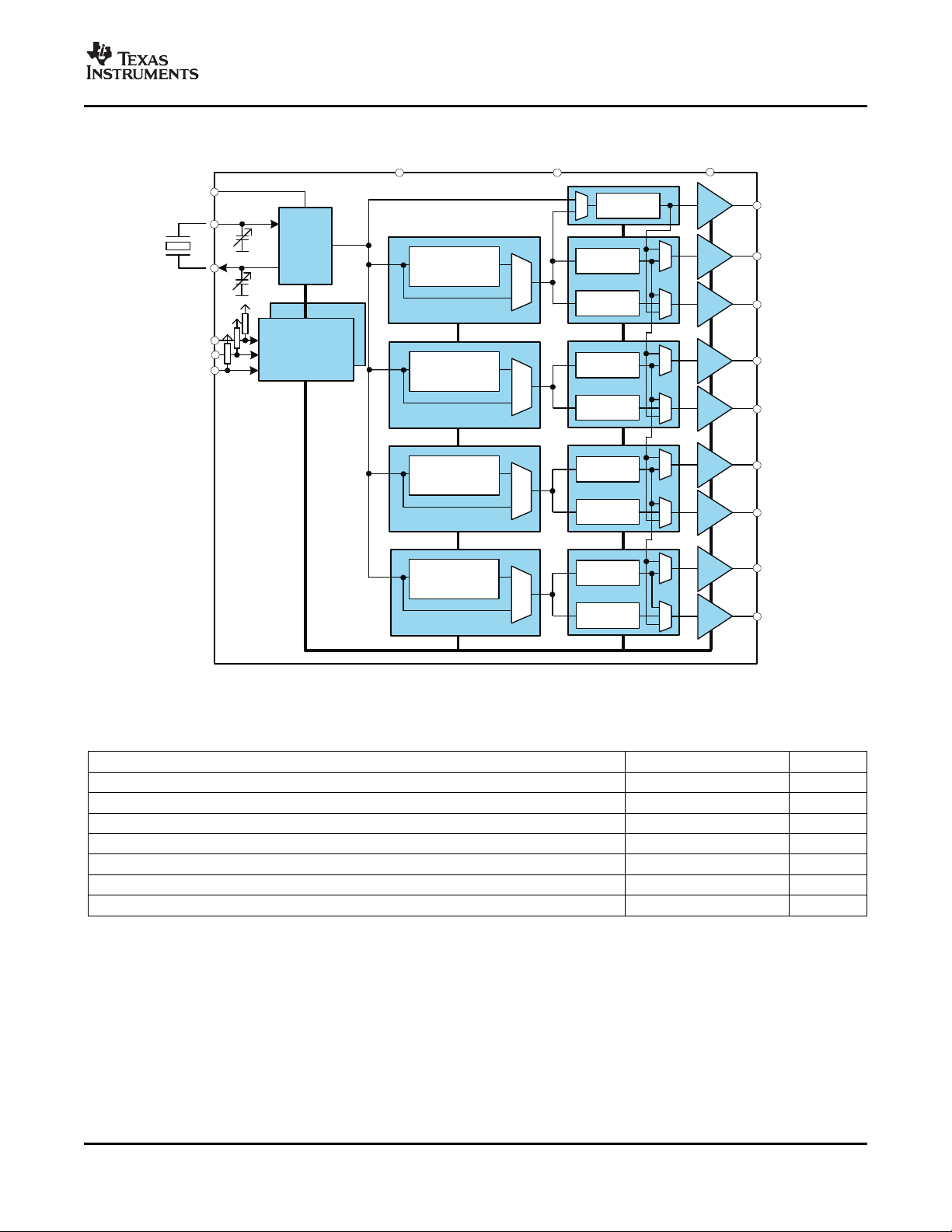
DESCRIPTION
The CDCE949 and CDCEL949 are modular PLL-based low cost, high-performance, programmable clock
synthesizers, multipliers and dividers. They generate up to 9 output clocks from a single input frequency. Each
output can be programmed in-system for any clock frequency up to 230 MHz, using up to four independent
configurable PLLs.
The CDCx949 has separate output supply pins, V
CDC E949.
The input accepts an external crystal or LVCMOS clock signal. If an external crystal is used, an on-chip load
capacitor is adequate for most applications. The value of the load capacitor is programmable from 0 to 20 pF.
Additionally, an on-chip VCXO is selectable, allowing synchronization of the output frequency to an external
control signal, i.e. a PWM signal.
The deep M/N divider ratio allows the generation of zero-ppm audio/video, networking (WLAN, BlueTooth™,
Ethernet, GPS) or Interface (USB, IEEE1394, Memory Stick) clocks from a reference input frequency such as
27-MHz.
All PLLs support SSC (Spread-Spectrum Clocking). SSC can be Center-Spread or Down-Spread clocking. This
is a common technique to reduce electro-magnetic interference (EMI).
Based on the PLL frequency and the divider settings, the internal loop-filter components are automatically
adjusted to achieve high stability, and to optimize the jitter-transfer characteristics of each PLL.
The device supports non-volatile EEPROM programming for easy customization of the device to the application.
It is preset to a factory-default configuration (see the Default Device Configuration section). It can be
reprogrammed to a different application configuration before PCB assembly, or reprogrammed by in-system
programming. All device settings are programmable through the SDA/SCL bus, a 2-wire serial interface.
Three programmable control inputs, S0, S1 and S2, can be used to control various aspects of operation
including frequency selection, changing the SSC parameters to lower EMI, PLL bypass, power down, and
choosing between low level or 3-state for the output-disable function.
The CDCx949 operates in a 1.8-V environment. It is characterized for operation from –40 ° C to 85 ° C.
, 1.8 V for the CDC EL949, and 2.5 V to 3.3 V for
DDOUT
DEVICE INFORMATION
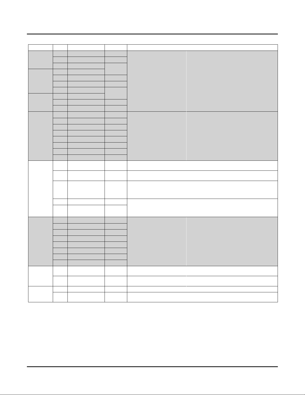
TERMINAL FUNCTIONS
TERMINAL
NAME NO. (TSSOP24)
Y1, Y2, ...Y9 O LVCMOS outputs
Xin/CLK 1 I Crystal oscillator input or LVCMOS clock input (selectable via SDA/SCL bus)
Xout 24 O Crystal oscillator output (leave open or pull up when not used)
V
Ctrl
V
DD
V
DDOUT
GND 5, 9, 14, 20 Ground Ground
S0 2 I User-programmable control input S0; LVCMOS inputs; internal pull-up 500 k Ω
SDA / S1 23 I/O / I pull-up 500 k Ω ; or
SCL / S2 22 I
2
21, 19, 18, 7, 8,
16, 15, 11, 12
4 I VCXO control voltage (leave open or pull up when not used)
3, 13 Power 1.8V power supply for the device
6, 10, 17 Power
I/O
CDCEL949: 1.8 V supply for all outputs
CDCE949: 3.3 V or 2.5 V supply for all outputs
SDA: Bi-directional serial data input/output (default configuration), LVCMOS; internal
S1: User-programmable control input; LVCMOS inputs; internal pull-up 500 k Ω
SCL: Serial clock input (default configuration), LVCMOS; internal pull-up 500 k Ω ; or
S2: User-programmable control input; LVCMOS inputs; internal pull-up 500 k Ω
Submit Documentation Feedback
www.ti.com
EEPROM
Xin/CLK
Xout
V
DD
GND
Vctr
V
DDOUT
VCXO
XO
LVCMOS
Y2
Y1
Y3
LV
CMOS
Pdiv1
10-Bit
Y4
Y5
Y6
Y7
Y8
Y9
LV
CMOS
Pdiv9
7-Bit
Pdiv8
7-Bit
M8
M9
LV
CMOS
LV
CMOS
Pdiv7
7-Bit
Pdiv6
7-Bit
M6
M7
LV
CMOS
LV
CMOS
Pdiv5
7-Bit
Pdiv4
7-Bit
M4
M5
LV
CMOS
LV
CMOS
Pdiv3
7-Bit
Pdiv2
7-Bit
M2
M3
LV
CMOS
Programming
and
SDA/SCL
Register
InputClock
M1
PLL Bypass
PLL 1
withSSC
MUX1
PLL Bypass
PLL 2
withSSC
MUX2
PLL Bypass
PLL 3
withSSC
MUX3
PLL Bypass
PLL 4
withSSC
M
U
X4
S0
S1/SDA
S2/SCL
FUNCTIONAL BLOCK DIAGRAM
CDCE949
CDCEL949
SCAS844 – JUNE 2007
ABSOLUTE MAXIMUM RATINGS
over operating free-air temperature range (unless otherwise noted)
V
V
V
I
I
I
O
T
stg
T
J
(1) Stresses beyond those listed under absolute maximum ratings may cause permanent damage to the device. These are stress ratings
(2) The input and output negative voltage ratings may be exceeded if the input and output clamp–current ratings are observed.
Supply voltage range –0.5 to 2.5 V
DD
Input voltage range
I
Output voltage range
O
Input current (Vi< 0, Vi> VDD) 20 mA
Continuous output current 50 mA
Storage temperature range –65 to 150 ° C
Maximum junction temperature 125 ° C
only and functional operation of the device at these or any other conditions beyond those indicated under recommended operating
conditions is not implied. Exposure to absolute–maximum–rated conditions for extended periods may affect device reliability.
(2)
(2)
Submit Documentation Feedback
(1)
VALUE UNIT
–0.5 to V
–0.5 to V
+ 0.5 V
DD
+ 0.5 V
DDOUT
3
www.ti.com
CDCE949
CDCEL949
SCAS844 – JUNE 2007
THERMAL RESISTANCE FOR TSSOP (PW) PACKAGE
PARAMETER
T
Thermal Resistance Junction to Ambient
JA
T
Thermal Resistance Junction to Case — 26
JC
(1) The package thermal impedance is calculated in accordance with JESD 51 and JEDEC2S2P (high-k board).
RECOMMENDED OPERATING CONDITIONS
V
V
V
V
V
V
V
IOH/I
C
T
DD
DD(OUT)
IL
IH
I(thresh)
IS
ICLK
OL
L
A
Device supply voltage 1.7 1.8 1.9 V
Output Yx supply
voltage
CDCE949 2.3 3.6
CDCEL949 1.7 1.9
Low level input voltage LVCMOS 0.3 × V
High level input voltage LVCMOS 0.7 × V
Input voltage threshold LVCMOS 0.5 × V
Input voltage range S0 0 1.9
Input voltage range S1, V
S2, SDA, SCL
= 0.5 V
Ithresh
DD
Input voltage range CLK 0 1.9 V
V
= 3.3 V ± 12 mA
DDout
Output current V
= 2.5 V ± 10 mA
DDout
V
= 1.8 V ± 8 mA
DDout
Output load LVCMOS 10 pF
Operating free-air temperature –40 85 ° C
(1)
AIRFLOW TSSOP24
(lfm) ° C/W
0 85
150 80
250 78
500 76
MIN NOM MAX UNIT
DD
DD
0 3.6
V
DD
V
V
V
V
RECOMMENDED CRYSTAL/VCXO SPECIFICATIONS
(1)
MIN NOM MAX UNIT
f
Xtal
Crystal Input frequency range (fundamental mode) 8 27 32 MHz
ESR Effective series resistance 100 Ω
f
PR
V
(Ctrl)
C0/C
C
L
Pulling range (0 V ≤ V
Ctrl
Frequency control voltage 0 V
Pullability ratio 220
1
On-chip load capacitance at Xin and Xout 0 20 pF
≤ 1.8 V)
(2)
± 120 ± 150 ppm
DD
(1) For more information about VCXO configuration and crystal recommendation see application report SCAA085 .
(2) Pulling range depends on crystal type, on-chip crystal load capacitance and PCB stray capacitance; pulling range of min ± 120 ppm
applies for crystal listed in the application report SCAA085 .
EEPROM SPECIFICATION
MIN TYP MAX UNIT
EEcyc EEcyc programming cycles of EEPROM 1000 cycles
EEret EEret data retention 10 years
V
4
Submit Documentation Feedback
www.ti.com
TIMING REQUIREMENTS
over recommended ranges of supply voltage, load and operating free-air temperature
CLK_IN Requirements MIN NOM MAX UNIT
f
tr/ t
duty
f
t
t
t
t
t
t
t
t
t
t
(CLK)
f
CLK
LVCMOS clock input frequency MHz
Rise and fall time CLK signal (20% to 80%) 3 ns
Duty cycle CLK at V
/ 2 40% 60%
DD
SDA/SCL TIMING REQUIREMENTS (see Figure 12 ) UNIT
(SCL)
su(START)
h(START)
w(SCLL)
w(SCLH)
h(SDA)
su(SDA)
r
f
su(STOP)
BUF
SCL clock frequency 0 100 0 400 kHz
START setup time (SCL high before SDA low) 4.7 0.6 μ s
START hold time (SCL low after SDA low) 4 0.6 μ s
SCL low-pulse duration 4.7 1.3 μ s
SCL high-pulse duration 4 0.6 μ s
SDA hold time (SDA valid after SCL low) 0 3.45 0 0.9 μ s
SDA setup time 250 100 ns
SCL/SDA input rise time 1000 300 ns
SCL/SDA input fall time 300 300 ns
STOP setup time 4.0 0.6 μ s
Bus free time between a STOP and START condition 4.7 1.3 μ s
PLL Bypass Mode 0 160
PLL Mode 8 160
CDCE949
CDCEL949
SCAS844 – JUNE 2007
STANDARD FAST
MODE MODE
MIN MAX MIN MAX
DEVICE CHARACTERISTICS
over recommended operating free-air temperature range (unless otherwise noted)
PARAMETER TEST CONDITIONS MIN TYP
OVERALL PARAMETER
I
DD
I
DD(OUT)
I
DD(PD)
V
f
VCO
f
OUT
Supply current (see Figure 3 ) mA
Supply current (see Figure 4 and No load, all outputs on,
Figure 5 ) f
Power down current. Every circuit
powered down except SDA/SCL
Supply voltage Vdd threshold for power
(PUC)
up control circuit
VCO frequency range of PLL 80 230 MHz
LVCMOS output frequency 230 MHz
LVCMOS PARAMETER
V
I
I
I
IH
I
IL
LVCMOS input voltage VDD = 1.7 V; II = –18 mA –1.2 V
IK
LVCMOS input current VI= 0 V or VDD; V
LVCMOS input current for S0/S1/S2 VI= VDD; V
LVCMOS input current for S0/S1/S2 VI= 0 V; V
Input capacitance at Xin/Clk V
C
Input capacitance at Xout V
I
Input capacitance at S0/S1/S2 VIS= 0 V or V
(1) All typical values are at respective nominal VDD.
All outputs off, f
MHz, f
out
= 135 MHz;
VCO
= 27 MHz
fIN= 0 MHz, V
DD
= 0 V or V
ICLK
= 0 V or V
IXout
= 27
CLK
= 1.9 V 50 μ A
DD
= 1.9 V ± 5 μ A
DD
= 1.9 V 5 μ A
DD
= 1.9 V –4 μ A
DD
DD
DD
All PLLs on 38
Per PLL 9
CDCE949
V
=3.3 V
DDOUT
CDCEL949
V
=1.8 V
DDOUT
0.85 1.45 V
(1)
MAX UNIT
4
2
6
2 pF
3
mA
Submit Documentation Feedback
5
www.ti.com
CDCE949
CDCEL949
SCAS844 – JUNE 2007
DEVICE CHARACTERISTICS (Continued)
over recommended operating free-air temperature range (unless otherwise noted)
PARAMETER TEST CONDITIONS MIN TYP
CDCE949 – LVCMOS PARAMETER FOR V
V
V
t
PLH
t
PHL
tr/t
t
jit(cc)
t
jit(per)
t
sk(o)
odc Output duty cycle
LVCMOS high-level output voltage V
OH
LVCMOS low-level output voltage V
OL
,
Propagation delay PLL bypass 3.2 ns
Rise and fall time V
f
Cycle-to-cycle jitter
Peak-to-peak period jitter
Output skew
(2) (3)
(2) (3)
(4)
(5)
CDCE949 – LVCMOS PARAMETER FOR V
V
V
t
PLH
t
PHL
tr/t
t
jit(cc)
t
jit(per)
t
sk(o)
odc Output duty cycle
LVCMOS high-level output voltage V
OH
LVCMOS low-level output voltage V
OL
,
Propagation delay PLL bypass 3.4 ns
Rise and fall time V
f
Cycle-to-cycle jitter
Peak-to-peak period jitter
Output skew
(2) (3)
(2) (3)
(4)
(5)
= 3.3 V – MODE
DDOUT
V
= 3 V, IOH= –0.1 mA 2.9
DDOUT
= 3 V, IOH= –8 mA 2.4 V
DDOUT
V
= 3 V, IOH= –12 mA 2.2
DDOUT
V
= 3 V, IOL= 0.1 mA 0.1
DDOUT
= 3 V, IOL= 8 mA 0.5 V
DDOUT
V
= 3 V, IOL= 12 mA 0.8
DDOUT
= 3.3 V (20%–80%) 0.6 ns
DDOUT
1 PLL switching, Y2-to-Y3 60 90
4 PLLs switching, Y2-to-Y9 120 170
1 PLL switching, Y2-to-Y3 70 100
4 PLLs switching, Y2-to-Y9 130 180
f
= 50 MHz; Y1-to-Y3 60
OUT
f
= 50 MHz; Y2-to-Y5 or Y6-to-Y9 160
OUT
f
= 100 MHz; Pdiv = 1 45 55 %
VCO
= 2.5 V – MODE
DDOUT
V
= 2.3 V, IOH= –0.1 mA 2.2
DDOUT
= 2.3 V, IOH= –6 mA 1.7 V
DDOUT
V
= 2.3 V, IOH= –10 mA 1.6
DDOUT
V
= 2.3 V, IOL= 0.1 mA 0.1
DDOUT
= 2.3 V, IOL= 6 mA 0.5 V
DDOUT
V
= 2.3 V, IOL= 10 mA 0.7
DDOUT
= 2.5 V (20%–80%) 0.8 ns
DDOUT
1 PLL switching, Y2-to-Y3 60 90 ps
4 PLLs switching, Y2-to-Y9 120 170
1 PLL switching, Y2-to-Y3 70 100 ps
4 PLLs switching, Y2-to-Y9 130 180
f
= 50 MHz; Y1-to-Y3 60
OUT
f
= 50 MHz; Y2-to-Y5 or Y6-to-Y9 160
OUT
f
= 100 MHz; Pdiv = 1 45 55 %
VCO
(1) All typical values are at respective nominal VDD.
(2) 10000 cycles.
(3) Jitter depends on device configuration. Data is taken under the following conditions: 1-PLL: fIN= 27 MHz, Y2/3 = 27 MHz, (measured at
Y2), 4-PLL: fIN= 27 MHz, Y2/3 = 27 MHz, (manured at Y2), Y4/5 = 16.384 MHz, Y6/7 = 74.25 MHz, Y8/9 = 48 MHz.
(4) The t
sampled on rising edge (tr).
specification is only valid for equal loading of each bank of outputs and outputs are generated from the same divider; data
sk(o)
(5) odc depends on output rise- and fall-time (tr/tf).
(1)
MAX UNIT
ps
ps
ps
ps
6
Submit Documentation Feedback
www.ti.com
10pF
1kW
LVCMOS
CDCE949
CDCEL949
1kW
LVCMOS LVCMOS
CDCE949
CDCEL949
Driver
Impedance
~50 W
LineImpedance
Zo=50 W
Series
Termination
(Optional)
CDCE949
CDCEL949
SCAS844 – JUNE 2007
DEVICE CHARACTERISTICS (Continued)
over recommended operating free-air temperature range (unless otherwise noted)
PARAMETER TEST CONDITIONS MIN TYP
SAVE THIS CDCEL949 – LVCMOS PARAMETER FOR V
V
DDOUT
V
V
t
PLH
t
PHL
tr/t
t
jit(cc)
t
jit(per)
t
sk(o)
odc Output duty cycle
LVCMOS high-level output voltage V
OH
LVCMOS low-level output voltage V
OL
,
Propagation delay PLL bypass 2.6 ns
Rise and fall time V
f
Cycle-to-cycle jitter
Peak-to-peak period jitter
Output skew
(2) (3)
(2) (3)
(4)
(5)
DDOUT
V
DDOUT
V
DDOUT
DDOUT
V
DDOUT
DDOUT
1 PLL switching, Y2-to-Y3 70 120 ps
4 PLLs switching, Y2-to-Y9 120 170
1 PLL switching, Y2-to-Y3 90 140 ps
4 PLLs switching, Y2-to-Y9 130 190
f
OUT
f
OUT
f
VCO
= 50 MHz; Y1-to-Y3 60 ps
= 50 MHz; Y2-to-Y5 or Y6-to-Y9 160
= 100 MHz; Pdiv = 1 45 55 %
= 1.8 V – MODE
DDOUT
= 1.7 V, IOH= –0.1 mA 1.6
= 1.7 V, IOH= –4 mA 1.4 V
= 1.7 V, IOH= –8 mA 1.1
= 1.7 V, IOL= 0.1 mA 0.1
= 1.7 V, IOL= 4 mA 0.3 V
= 1.7 V, IOL= 8 mA 0.6
= 1.8 V (20%–80%) 0.7 ns
SDA/SCL PARAMETER
V
I
IH
V
V
V
C
SCL and SDA input clamp voltage V
IK
SCL and SDA input current VI= VDD; V
SDA/SCL input high voltage
IH
SDA/SCL input low voltage
IL
SDA low-level output voltage IOL= 3 mA, V
OL
SCL/SDA input capacitance VI= 0 V or V
I
(6)
(6)
= 1.7 V; II= –18 mA –1.2 V
DD
= 1.9 V ± 10 μ A
DD
0.7 V
DD
= 1.7 V V
DD
DD
(1) All typical values are at respective nominal VDD.
(2) 10000 cycles.
(3) Jitter depends on device configuration. Data is taken under the following conditions: 1-PLL: fIN= 27 MHz, Y2/3 = 27 MHz, (measured at
Y2), 4-PLL: fIN= 27 MHz, Y2/3 = 27 MHz, (measured at Y2), Y4/5 = 16.384 MHz, Y6/7 = 74.25 MHz, Y8/9 = 48 MHz.
(4) The t
sampled on rising edge (tr).
specification is only valid for equal loading of each bank of outputs and outputs are generated from same divider; data
sk(o)
(5) odc depends on output rise- and fall-time (tr/tf).
(6) SDA and SCL pins are 3.3-V tolerant.
(1)
MAX UNIT
0.3
V
DD
0.2
V
DD
3 10 pF
V
V
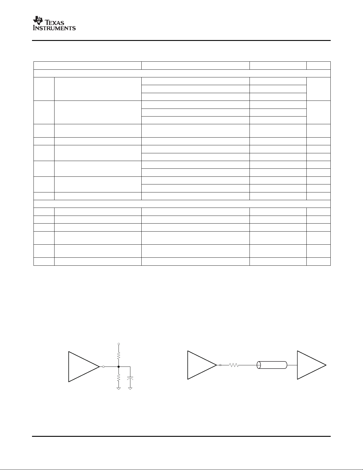
PARAMETER MEASUREMENT INFORMATION
Figure 1. Test Load Figure 2. Test Load for 50 Ω Board Environment
Submit Documentation Feedback
7
www.ti.com
0
10
20
30
40
50
60
70
80
90
100
10 60 110 160 210
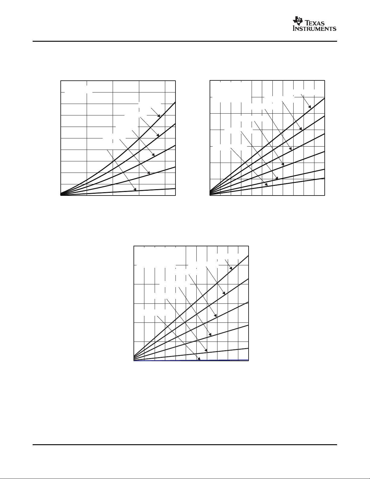
PLL -Frequency-MHz
I
-SupplyCurrent-mA
D
D
3PLL on
V =1.8V
DD
allPLL off
1PLL on
4PLL on
2PLL on
0
5
10
15
20
25
30
35
10 30 50 70 90 110 130 150 170 190 210 230
f -OutputFrequency-MHz
OUT
I -mA
D
DOUT
alloutputsoff
9outputson
7outputson
5outputson
3outputson
1outputon
V =1.8V,
V =3.3V,
NoLoad
DD
DDOUT
10 30 50 70 90 110 130 150 170 190 210 230
f -OutputFrequency-MHz
OUT
I -mA
D
DOUT
0
2
4
6
8
10
12
alloutputsoff
9outputson
7outputson
5outputson
3outputson
1outputon
V =1.8V,
V =1.8V,
NoLoad
DD
DDOUT
CDCE949
CDCEL949
SCAS844 – JUNE 2007
TYPICAL CHARACTERISTICS
CDCE949 AND CDCEL949 SUPPLY CURRENT CDCE949 OUTPUT CURRENT
vs vs
PLL FREQUENCY OUTPUT FREQUENCY
Figure 3. Figure 4.
CDCEL949 OUTPUT CURRENT
vs
OUTPUT FREQUENCY
8
Figure 5.
Submit Documentation Feedback
www.ti.com
APPLICATION INFORMATION
Control Terminal Configuration
The CDCE949/CDCEL949 has three user-definable control terminals (S0, S1 and S2) which allow external
control of device settings. They can be programmed to perform any of the following functions:
• Spread-Spectrum Clocking selection: Spread-type and spread-amount selection
• Frequency selection: Switching between any of two user-defined frequencies
• Output-State selection: Output configuration and power-down control
The user can predefine up to eight different control settings. Table 1 and Table 2 explain these settings.
Table 1. Control Terminal Definition
External Control-Bits PLL1 Setting PLL2 Setting PLL3 Setting PLL4 Setting Y1 Setting
Control Function
CDCE949
CDCEL949
SCAS844 – JUNE 2007
SSC Selection
PLL Frequency Selection
Output Y2/Y3 Selection
SSC Selection
PLL Frequency Selection
Output Y4/Y5 Selection
PLL Frequency Selection
SSC Selection
Output Y6/Y7 Selection
PLL Frequency Selection
SSC Selection
Table 2. PLLx Setting (can be selected for each PLL individual)
SSC Selection (Center/Down)
SSCx [3-bits] Center Down
0 0 0 0% (off) 0% (off)
0 0 1 ± 0.25% –0.25%
0 1 0 ± 0.5% –0.5%
0 1 1 ± 0.75% –0.75%
1 0 0 ± 1.0% –1.0%
1 0 1 ± 1.25% –1.25%
1 1 0 ± 1.5% –1.5%
1 1 1 ± 2.0% –2.0%
FREQUENCY SELECTION
FSx FUNCTION
0 Frequency0
1 Frequency1
OUTPUT SELECTION
YxYx FUNCTION
0 State0
1 State1
(1) Center/Down-Spread, Frequency0/1 and State0/1 are user-definable in PLLx Configuration Register;
(2) Frequency0 and Frequency1 can be any frequency within the specified f
(3) State0/1 selection is valid for both outputs of the corresponding PLL module and can be power down,
3-state, low or active
(2)
(3)
(Y2 ... Y9)
range.
VCO
Output Y8/Y9 Selection
Output Y1 and Power Down Selection
(1)
Submit Documentation Feedback
9

EEPROM
Xin
Xout
V
DD
GND
V
DDOUT
X-tal
Y2=27MHz
Y1=27MHz
Y3=27MHz
LV
CMOS
Pdiv1=1
Y4=27MHz
Y5=27MHz
Y6=27MHz
Y7=27MHz
Y8=27MHz
Y9=27MHz
LV
CMOS
Pdiv9=1
Pdiv8=1
M8
M9
LV
CMOS
LV
CMOS
Pdiv7=1
Pdiv6=1
M6
M7
LV
CMOS
LV
CMOS
Pdiv5=1
Pdiv4=1
M4
M5
LV
CMOS
LV
CMOS
Pdiv3=1
Pdiv2=1
M2
M3
LV
CMOS
Programming
and
SDA/SCL
Register
InputClock
M1
PLL Bypass
PLL 1
powerdown
MUX1
PLL Bypass
PLL 2
powerdown
MUX2
PLL Bypass
PLL 3
powerdown
MUX3
PLL Bypass
PLL 4
powerdown
MUX4
S0
SDA
SCL
27MHz
Crystal
ProgrammingBus
“1” =outputsenabled
“0” =outputs3-State
CDCE949
CDCEL949
SCAS844 – JUNE 2007
Table 3. Y1 Setting
Y1 SELECTION
Y1 FUNCTION
0 State 0
1 State 1
(1) State0 and State1 are user-definable in Generic Configuration
Register and can be power down, 3-state, low or active.
The S1/SDA and S2/SCL pins of the CDCE949/CDCEL949 are dual-function pins. In the default configuration
they are defined as SDA/SCL for the serial interface. They can be programmed as control pins (S1/S2) by
setting the appropriate bits in the EEPROM. Note that changes to the Control register (Bit [6] of Byte 02) have
no effect until they are written into the EEPROM.
Once they are set as control pins, the serial programming interface is no longer available. However, if V
forced to GND, the two control-pins, S1 and S2, temporarily act as serial programming pins (SDA/SCL).
S0 is not a multi-use pin, it is a control pin only.
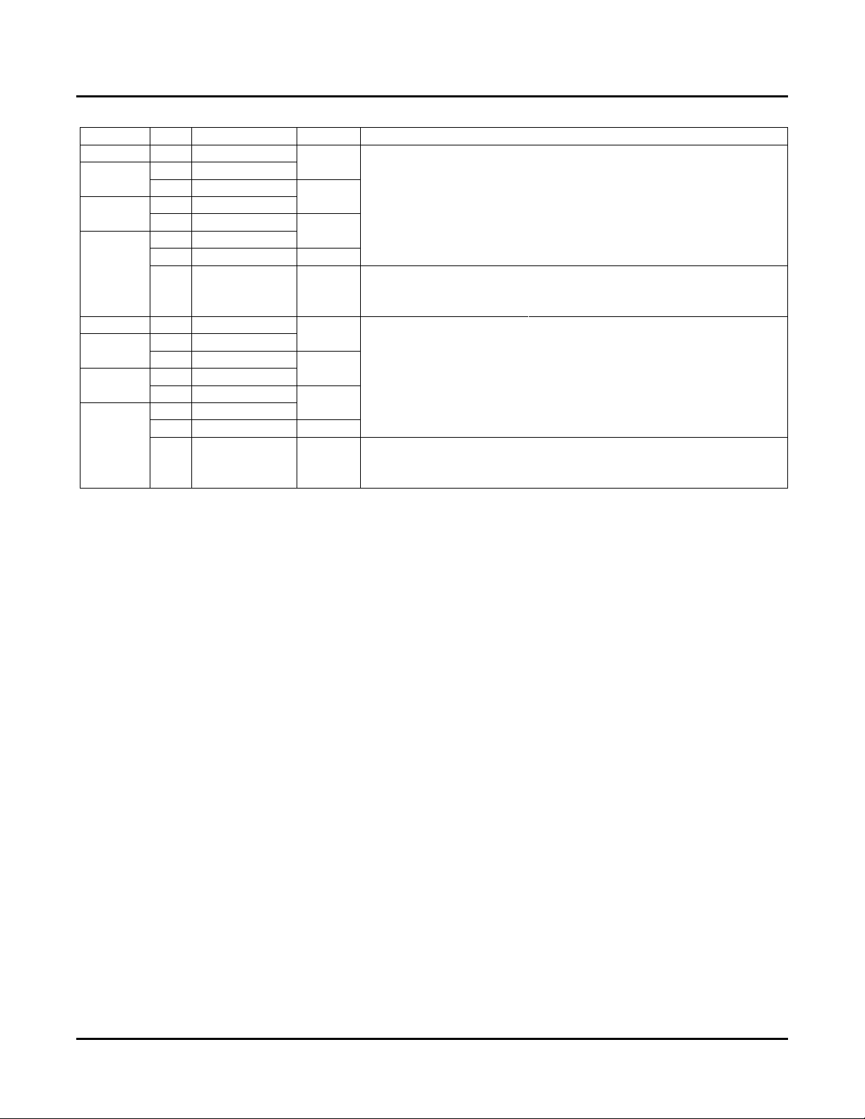
DEFAULT DEVICE SETTING
The internal EEPROM of CDCE949/CDCEL949 is preconfigured as shown in Figure 6 . (The input frequency is
passed through to the output as a default.) This allows the device to operate in default mode without the extra
production step of programming it. The default setting appears after power is supplied or after a power-down/up
sequence until it is reprogrammed by the user to a different application configuration. A new register setting is
programmed via the serial SDA/SCL Interface.
(1)
DDOUT
is
A different default setting can be programmed upon customer request. Contact Texas Instruments sales or
Figure 6. Default Configuration
marketing representative for more information.
Table 4 shows the default setting for the Control Terminal Register (external control pins). In normal operation,
all 8 register settings are available, but in the default configuration only the first two settings (0 and 1) can be
selected with S0, as S1 and S2 are configured as programming pins in default mode.
10
Submit Documentation Feedback

CDCE949
CDCEL949
SCAS844 – JUNE 2007
Table 4. Factory Default Setting for Control Terminal Register
EXTERNAL
CONTROL-PINS
S2 S1 S0 Y1 FS1 SSC1 Y2Y3 FS2 SSC2 Y4Y5 FS3 SSC3 Y6Y7 FS4 SSC4 Y8Y9
SCL (I2C) SDA (I2C)
SCL (I2C) SDA (I2C)
(1) In default mode or when programmed respectively, S1 and S2 act as a serial programming interface, SDA/SCL. In this mode, they have
no control-pin function, but are internally interpreted as if S1=0 and S2=0. S0, however, is a control-pin which in the default mode
switches all outputs ON or OFF (as pre-defined above).
(1)
SDA/SCL SERIAL INTERFACE
The CDCE949/CDCEL949 operates as a slave device on the 2-wire serial SDA/SCL bus, compatible with the
popular SMBus or I2C™ specification. It operates in the standard-mode transfer (up to 100 kbps) and fast-mode
transfer (up to 400 kbps) and supports 7-bit addressing.
The S1/SDA and S2/SCL pins of the CDC9xx are dual-function pins. In the default configuration they are used
as SDA/SCL serial programming interface. They can be reprogrammed as general purpose control pins, S1 and
S2, by changing the corresponding EEPROM setting, Byte 02, Bit [6].
DATA PROTOCOL
The device supports Byte Write and Byte Read and Block Write and Block Read operations.
For Byte Write/Read operations, the system controller can individually access addressed bytes.
For Block Write/Read operations, the bytes are accessed in sequential order from lowest to highest byte (with
most significant bit first) with the ability to stop after any complete byte has been transferred. The number of
bytes read out is defined by the Byte Count field in the Generic Configuration Register. During a Block Read
instruction, the entire number of bytes defined in Byte Count must be read out to correctly finish the read cycle.
When a byte is sent to the device, it is written into the internal register and immediately takes effect. This applies
to each transferred byte, whether in a Byte Write or a Block Write sequence.
If the EEPROM Write Cycle is initiated, the internal SDA register contents are written into the EEPROM. During
this write cycle, data is not accepted at the SDA/SCL bus until the write cycle is completed. However, data can
be read during the programming sequence (Byte Read or Block Read). The programming status can be
monitored by reading EEPIP, Byte 01–Bit [6].
The offset of the indexed byte is encoded in the command code, as described in Table 6 .
Y1 PLL1 SETTING PLL2 SETTING PLL3 SETTING PLL4 SETTING
Output Freq. SSC Output Freq. SSC Output Freq. SSC Output Freq. SSC Output
Select Select Sel. Select Select Sel. Select Select Sel. Select Select Sel. Select
0 3-State f
1 enabled f
VCO1_0
VCO1_0
off 3-State f
off enabled f
VCO2_0
VCO2_0
off 3-State f
off enabled f
VCO3_0
VCO3_0
off 3-State f
off enabled f
VCO4_0
VCO4_0
off 3-State
off enabled
Table 5. Slave Receiver Address (7 bits)
Device A6 A5 A4 A3 A2 A1
CDCE913/CDCEL913 1 1 0 0 1 0 1 1/0
CDCE925/CDCEL925 1 1 0 0 1 0 0 1/0
CDCE937/CDCEL937 1 1 0 1 1 0 1 1/0
CDCE949/CDCEL949 1 1 0 1 1 0 0 1/0
(1) Address bits A0 and A1 are programmable via the SDA/SCL bus (Byte 01, Bit [1:0]. This allows addressing up to 4 devices connected to
the same SDA/SCL bus. The least significant bit of the address byte designates a write or read operation.
Submit Documentation Feedback
(1)
(1)
A0
R/ W
11

1 7 1 1 8 1 1
S Slave Address A DataByte A P
MSB LSB MSB LSB
S StartCondition
Sr RepeatedStartCondition
1=Read(Rd)fromCDCE9xxdevice;0=Write(Wr)totheCDCE9xxx
A Acknowledg(ACK=0andNACK=1)
P StopCondition
MastertoSlave Transmission
SlavetoMaster Transmission
R/W
R/W
1 7 1 1 8 1 1 1
S Slave Address Wr A A A PDataByteCommandCode
8
1 7 1 1 1 1 1 1
S Slave Address Wr A A S Rd A
8 1 1
DataByte A P
CommandCode
8 7
Slave Address
1 7 1 1 1 1
S Slave Address Wr A A A
8 1 1 1 1
DataByte0 A A A P
8
DataByteN-1…
8
DataByte1
8
CommandCode ByteCount=N
8
CDCE949
CDCEL949
SCAS844 – JUNE 2007
Table 6. Command Code Definition
BIT DESCRIPTION
7
(6:0) Byte Offset for Byte Read, Block Read, Byte Write and Block Write operation.
Generic Programming Sequence
0 = Block Read or Block Write operation
1 = Byte Read or Byte Write operation
Byte Write Programming Sequence
Byte Read Programming Sequence
Block Write Programming Sequence
Figure 7. Generic Programming Sequence
Figure 8. Byte Write Protocol
Figure 9. Byte Read Protocol
NOTE: Data Byte 0 Bits [7:0] is reserved for Revision Code and Vendor Identification. Also it is used for internal test purpose
and should not be overwritten.
12
Figure 10. Block Write Programming
Submit Documentation Feedback

Block Read Programming Sequence
1 7 1 1 1 1 1 1
S Slave Address Wr A A Sr Rd A
8 1 1 1 1
ByteCountN A A A PDataByte0 … DataByteN-1
8
CommandCode
7
Slave Address
8 8
P S P
t
(BUS)
t
w(SCLL)tw(SCLH)
t
r
t
f
t
h(START)
t
SU(SDA)
t
h(SDA)
t
SU(STOP)
t
SU(START)
t
r
t
f
SCL
SDA
V
IH
V
IL
V
IH
V
IL
A
Bit7(MSB)
Bit6 Bit0(LSB)
R
P
Master
R
P
SDA
SCL
C
BUS
Slave
CDCE949
CDCEL949
C
BUS
Figure 11. Block Read Protocol
Timing Diagram for the SDA/SCL Serial Control Interface
CDCE949
CDCEL949
SCAS844 – JUNE 2007
Figure 12. Timing Diagram for the SDA/SCL Serial Control Interface
SDA/SCL Hardware Interface
Figure 13 shows how the CDCE949/CDCEL949 clock synthesizer is connected to the SDA/SCL serial interface
bus. Multiple devices can be connected to the bus but the speed may need to be reduced (400 kHz is the
maximum) if many devices are connected.
Note that the pull-up resistor value (R
connected devices. The recommended pull-up value is 4.7 k Ω . It must meet the minimum sink current of 3 mA
at V
= 0.4 V for the output stages (for more details see the SMBus or I2C Bus specification).
OLmax
) depends on the supply voltage, bus capacitance and number of
P
Figure 13. SDA/SCL Hardware Interface
Submit Documentation Feedback
13

CDCE949
CDCEL949
SCAS844 – JUNE 2007
SDA/SCL CONFIGURATION REGISTERS
The clock input, control pins, PLLs and output stages are user configurable. The following tables and
explanations describe the programmable functions of the CDCE949/CDCEL949. All settings can be manually
written to the device via the SDA/SCL bus, or are easily programmable by using the TI Pro Clock software. TI
Pro Clock software allows the user to quickly make all settings and automatically calculates the values for
optimized performance at lowest jitter.
Table 7. SDA/SCL Registers
ADDRESS OFFSET REGISTER DESCRIPTION TABLE
00h Generic Configuration Register Table 9
10h PLL1 Configuration Register Table 10
20h PLL2 Configuration Register Table 11
30h PLL3 Configuration Register Table 12
40h PLL4 Configuration Register Table 13
The grey-highlighted Bits described in the Configuration Registers tables on the following pages, belong to the
Control Terminal Register. The user can predefine up to eight different control settings. These settings can then
be selected by the external control pins, S0, S1, and S2 (See the Control Terminal Configuration section).
Table 8. Configuration Register, External Control Terminals
EXTERNAL
CONTROL
PINS
S2 S1 S0 Y1 FS1 SSC1 Y2Y3 FS2 SSC2 Y4Y5 FS3 SSC3 Y6Y7 FS4 SSC4 Y8Y9
0 0 0 Y1_0 FS1_0 SSC1_0 Y2Y3_0 FS2_0 SSC2_0 Y4Y5_0 FS3_0 SSC3_0 Y6Y7_0 FS4_0 SSC4_0 Y8Y9_0
0 0 1 Y1_1 FS1_1 SSC1_1 Y2Y3_1 FS2_1 SSC2_1 Y4Y5_1 FS3_1 SSC3_1 Y6Y7_1 FS4_1 SSC4_1 Y8Y9_1
0 1 0 Y1_2 FS1_2 SSC1_2 Y2Y3_2 FS2_2 SSC2_2 Y4Y5_2 FS3_2 SSC3_2 Y6Y7_2 FS4_2 SSC4_2 Y8Y9_2
0 1 1 Y1_3 FS1_3 SSC1_3 Y2Y3_3 FS2_3 SSC2_3 Y4Y5_3 FS3_3 SSC3_3 Y6Y7_3 FS4_3 SSC4_3 Y8Y9_3
1 0 0 Y1_4 FS1_4 SSC1_4 Y2Y3_4 FS2_4 SSC2_4 Y4Y5_4 FS3_4 SSC3_4 Y6Y7_4 FS4_4 SSC4_4 Y8Y9_4
1 0 1 Y1_5 FS1_5 SSC1_5 Y2Y3_5 FS2_5 SSC2_5 Y4Y5_5 FS3_5 SSC3_5 Y6Y7_5 FS4_5 SSC4_5 Y8Y9_5
1 1 0 Y1_6 FS1_6 SSC1_6 Y2Y3_6 FS2_6 SSC2_6 Y4Y5_6 FS3_6 SSC3_6 Y6Y7_6 FS4_6 SSC4_6 Y8Y9_6
1 1 1 Y1_7 FS1_7 SSC1_7 Y2Y3_7 FS2_7 SSC2_7 Y4Y5_7 FS3_7 SSC3_7 Y6Y7_7 FS4_7 SSC4_7 Y8Y9_7
Addr.
Offset
(1) Address Offset refers to the byte address in the Configuration Register on following pages.
Y1 PLL1 SETTING PLL2 SETTING PLL3 SETTING PLL4 SETTING
Output Freq. SSC Output Freq. SSC Output Freq. SSC Output Freq. SSC Output
Select Select Select Select Select Select Select Select Select Select Select Select Select
04h 13h 10h-12h 15h 23h 20h-22h 25h 33h 30h-32h 35h 43h 40h-42h 45h
(1)
14
Submit Documentation Feedback

Xin
Xout
Vctr
VCXO
XO
20pF
20pF
i.e.
XCSEL =10pF
Table 9. Generic Configuration Register
(1)
OFFSET
(2)
Bit
Acronym Default
00h 7 E_EL xb Device Identification (read only): ‘1’ is CDCE949 (3.3V), ‘0’ is CDCEL949 (1.8V)
6:4 RID 0h Revision Identification Number (read only)
3:0 VID 1h Vendor Identification Number (read only)
01h 7 – 0b Reserved - always write 0
6 EEPIP 0b
5 EELOCK 0b
4 PWDN 0b
3:2 INCLK 00b
1:0 SLAVE_ADR 00b Programmable Address Bits A0 and A1 of the Slave Receiver Address
02h Clock source selection for output Y1: 0 – input clock
7 M1 1b
6 SPICON 0b
5:4 Y1_ST1 11b Y1-State0/1 Definition (applies to Y1_ST1 and Y1_ST0)
3:2 Y1_ST0 01b
1:0 Pdiv1 [9:8] 10-Bit Y1-Output-Divider Pdiv1: 0 – divider reset and stand-by
03h 7:0 Pdiv1 [7:0]
04h 7 Y1_7 0b Y1_x State Selection
6 Y1_6 0b 0 – State0 (predefined by Y1-State0 Definition [Y1_ST0])
5 Y1_5 0b
4 Y1_4 0b
3 Y1_3 0b
2 Y1_2 0b
1 Y1_1 1b
0 Y1_0 0b
05h Crystal load capacitor 00h → 0 pF
7:3 XCSEL 0Ah
(3)
EEPROM Programming 0 – EEPROM programming is completed
(4)
Status
: (read only) 1 – EEPROM is in programming mode
Permanently Lock EEPROM 0 – EEPROM is not locked
(5)
Data
: 1 – EEPROM will be permanently locked
DESCRIPTION
Device power down (overwrites S0/S1/S2 setting; configuration register settings are unchanged)
0 – device active (all PLLs and all outputs are enabled)
1 – device power down (all PLLs in power down and all outputs in 3-State)
Input clock selection: 00 – X-tal 10 – LVCMOS
01 – VCXO 11 – reserved
Operation mode selection for pin 22/23
(6)
0 – serial programming interface SDA (pin 23) and SCL (pin 22)
1 – control pins S1 (pin 23) and S2 (pin 22)
00 – device power down (all PLLs in power down and all outputs in 3-state)
01 – Y1 disabled to 3-state
10 – Y1 disabled to low
11 – Y1 enabled (normal operation)
001h
(7)
1-to-1023 – divider value
1 – State1 (predefined by Y1-State1 Definition [Y1_ST1])
(8)
selection
: 01h → 1 pF
02h → 2 pF
14h-to-1Fh → 20 pF
CDCE949
CDCEL949
SCAS844 – JUNE 2007
1 – PLL1 clock
2:0 — 0b Reserved - do not write others than 0
(1) Writing data beyond ‘50h’ may adversely affect device function.
(2) All data is transferred MSB-first.
(3) Unless custom setting is used.
(4) During EEPROM programming, no data is allowed to be sent to the device via the SDA/SCL bus until the programming sequence is
completed. Data, however, can be read during the programming sequence (Byte Read or Block Read).
(5) If this bit is set high in the EEPROM, the actual data in the EEPROM is permanently locked, and no further programming is possible.
Data, however can still be written via SDA/SCL bus to the internal register to change device function on the fly. But new data can no
longer be saved to the EEPROM. EELOCK is effective only if written into the EEPROM
(6) Selection of control-pins is effective only if written into the EEPROM. Once written into the EEPROM, the serial programming pins are
no longer available. However, if V
(SDA/SCL), and the two slave receiver address bits are reset to A0 = 0 and A1 = 0.
is forced to GND, the two control-pins, S1 and S2, temporally act as serial programming pins
DDOUT
(7) These are the bits of the Control Terminal Register. The user can pre-define up to eight different control settings. These settings can
then be selected by the external control pins, S0, S1, and S2.
(8) The internal load capacitor (C
a fine adjustment of CLby few pF. The value of CLcan be programmed with a resolution of 1 pF for a total crystal load range of 0 pF to
, C2) must be used to achieve the best clock performance. External capacitors should be used only to do
1
20 pF. For CL> 20 pF use additional external capacitors. Also, the device input capacitance must be considered; this adds 1.5 pF
(6pF//2pF) to the selected CL. For more information about VCXO configuration and crystal recommendations, see application report
SCAA085
Submit Documentation Feedback
15

CDCE949
CDCEL949
SCAS844 – JUNE 2007
Table 9. Generic Configuration Register (continued)
(1)
OFFSET
06h 7-Bit Byte Count (Defines the number of Bytes which will be sent from this device at the next Block
07h-0Fh — — 0h Reserved – do not write others than 0
(2)
Bit
Acronym Default
7:1 BCOUNT 50h
0 EEWRITE 0b
(9) NOTE: The EEPROM WRITE bit must be sent last. This ensures that the content of all internal registers are written into the EEPROM.
The EEWRITE cycle is initiated by the rising edge of the EEWRITE-Bit. A static level high does not trigger an EEPROM WRITE cycle.
The EEWRITE-Bit must be reset low after the programming is completed. The programming status can be monitored by readout EEPIP.
If EELOCK is set high, no EEPROM programming will be possible.
(3)
Read transfer; all bytes must be read out to correctly finish the read cycle.)
Initiate EEPROM Write Cycle
0 – no EEPROM write cycle
1 – start EEPROM write cycle (internal configuration register are saved to the EEPROM)
(4) (9)
DESCRIPTION
16
Submit Documentation Feedback

SCAS844 – JUNE 2007
Table 10. PLL1 Configuration Register
(1)
OFFSET
10h 7:5 SSC1_7 [2:0] 000b SSC1: PLL1 SSC Selection (Modulation Amount)
11h 7 SSC1_5 [0]
12h 7:6 SSC1_2 [1:0]
13h
14h PLL1 Multiplexer: 0 – PLL1
15h
16h PLL1 SSC down/center selection: 0 – down
17h 7 — 0b Reserved – do not write others than 0
(1) Writing data beyond 50h may adversely affect device function.
(2) All data is transferred MSB-first.
(3) Unless a custom setting is used
(4) The user can pre-define up to eight different control settings. In normal device operation, these settings can be selected by the external
control pins, S0, S1, and S2.
(2)
Bit
4:2 SSC1_6 [2:0] 000b Down Center
1:0 SSC1_5 [2:1]
6:4 SSC1_4 [2:0] 000b
3:1 SSC1_3 [2:0] 000b
0 SSC1_2 [2]
5:3 SSC1_1 [2:0] 000b
2:0 SSC1_0 [2:0] 000b
7 FS1_7 0b
6 FS1_6 0b 0 – f
5 FS1_5 0b
4 FS1_4 0b
3 FS1_3 0b
2 FS1_2 0b
1 FS1_1 0b
0 FS1_0 0b
7 MUX1 1b
6 M2 1b
5:4 M3 10b
3:2 Y2Y3_ST1 11b Y2, 00 – Y2/Y3 disabled to 3-State (PLL1 is in power down)
1:0 Y2Y3_ST0 01b
7 Y2Y3_7 0b
6 Y2Y3_6 0b 0 – state0 (predefined by Y2Y3_ST0)
5 Y2Y3_5 0b
4 Y2Y3_4 0b
3 Y2Y3_3 0b
2 Y2Y3_2 0b
1 Y2Y3_1 1b
0 Y2Y3_0 0b
7 SSC1DC 0b
6:0 Pdiv2 01h
6:0 Pdiv3 01h
Acronym Default
(3)
000 (off) 000 (off)
000b
000b
001 – 0.25% 001 ± 0.25%
010 – 0.5% 010 ± 0.5%
011 – 0.75% 011 ± 0.75%
100 – 1.0% 100 ± 1.0%
101 – 1.25% 101 ± 1.25%
110 – 1.5% 110 ± 1.5%
111 – 2.0% 111 ± 2.0%
FS1_x: PLL1 Frequency Selection
(predefined by PLL1_0 – Multiplier/Divider value)
VCO1_0
1 – f
Output Y2 Multiplexer: 0 – Pdiv1
Output Y3 Multiplexer: 00 – Pdiv1-Divider
Y3-State0/1definition: 01 – Y2/Y3 disabled to 3-State (PLL1 on)
Y2Y3_x Output State Selection
1 – state1 (predefined by Y2Y3_ST1)
7-Bit Y2-Output-Divider Pdiv2: 0 – reset and stand-by
7-Bit Y3-Output-Divider Pdiv3: 0 – reset and stand-by
(predefined by PLL1_1 – Multiplier/Divider value)
VCO1_1
1 – PLL1 Bypass (PLL1 is in power down)
1 – Pdiv2
01 – Pdiv2-Divider
10 – Pdiv3-Divider
11 – reserved
10–Y2/Y3 disabled to low (PLL1 on)
11 – Y2/Y3 enabled (normal operation, PLL1 on)
DESCRIPTION
(4)
(4)
(4)
1 – center
1-to-127 – divider value
1-to-127 – divider value
CDCE949
CDCEL949
Submit Documentation Feedback
17

CDCE949
CDCEL949
SCAS844 – JUNE 2007
Table 10. PLL1 Configuration Register (continued)
(1)
OFFSET
18h 7:0 PLL1_0N [11:4 PLL1_0: 30-Bit Multiplier/Divider value for frequency f
19h 7:4 PLL1_0N [3:0]
1Ah 7:3 PLL1_0R[4:0]
1Bh 7:5 PLL1_0Q [2:0]
1Ch 7:0 PLL1_1N [11:4] PLL1_1: 30-Bit Multiplier/Divider value for frequency f
1Dh 7:4 PLL1_1N [3:0]
1Eh 7:3 PLL1_1R[4:0]
1Fh 7:5 PLL1_1Q [2:0]
(2)
Bit
Acronym Default
3:0 PLL1_0R [8:5]
2:0 PLL1_0Q [5:3]
4:2 PLL1_0P [2:0] 010b
1:0 VCO1_0_RANGE 00b
3:0 PLL1_1R [8:5]
2:0 PLL1_1Q [5:3]
4:2 PLL1_1P [2:0] 010b
1:0 VCO1_1_RANGE 00b
(3)
004h
(for more information see PLL Multiplier/Divider Definition )
000h
10h
f
range selection: 00 – f
VCO1_0
004h
(for more information see paragraph PLL Multiplier/Divider Definition)
000h
10h
f
range selection: 00 – f
VCO1_1
DESCRIPTION
< 125 MHz
VCO1_0
01 – 125 MHz ≤ f
10 – 150 MHz ≤ f
11 – f
01 – 125 MHz ≤ f
≥ 175 MHz
VCO1_0
< 125 MHz
VCO1_1
10 – 150 MHz ≤ f
11 – f
≥ 175 MHz
VCO1_1
VCO1_0
< 150 MHz
VCO1_0
< 175 MHz
VCO1_0
VCO1_1
< 150 MHz
VCO1_1
< 175 MHz
VCO1_1
18
Submit Documentation Feedback

SCAS844 – JUNE 2007
Table 11. PLL2 Configuration Register
(1)
OFFSET
20h 7:5 SSC2_7 [2:0] 000b SSC2: PLL2 SSC Selection (Modulation Amount)
21h 7 SSC2_5 [0]
22h 7:6 SSC2_2 [1:0]
23h
24h PLL2 Multiplexer: 0 – PLL2
25h
26h PLL2 SSC down/center selection: 0 – down
27h 7 — 0b Reserved – do not write others than 0
(1) Writing data beyond 50h may adversely affect device function.
(2) All data is transferred MSB-first.
(3) Unless a custom setting is used
(4) The user can pre-define up to eight different control settings. In normal device operation, these settings can be selected by the external
control pins, S0, S1, and S2.
(2)
Bit
4:2 SSC2_6 [2:0] 000b Down Center
1:0 SSC2_5 [2:1]
6:4 SSC2_4 [2:0] 000b
3:1 SSC2_3 [2:0] 000b
0 SSC2_2 [2]
5:3 SSC2_1 [2:0] 000b
2:0 SSC2_0 [2:0] 000b
7 FS2_7 0b
6 FS2_6 0b 0 – f
5 FS2_5 0b
4 FS2_4 0b
3 FS2_3 0b
2 FS2_2 0b
1 FS2_1 0b
0 FS2_0 0b
7 MUX2 1b
6 M4 1b
5:4 M5 10b
3:2 Y4Y5_ST1 11b Y4, 00 – Y4/Y5 disabled to 3-State (PLL2 is in power down)
1:0 Y4Y5_ST0 01b
7 Y4Y5_7 0b
6 Y4Y5_6 0b 0 – state0 (predefined by Y4Y5_ST0)
5 Y4Y5_5 0b
4 Y4Y5_4 0b
3 Y4Y5_3 0b
2 Y4Y5_2 0b
1 Y4Y5_1 1b
0 Y4Y5_0 0b
7 SSC2DC 0b
6:0 Pdiv4 01h
6:0 Pdiv5 01h
Acronym Default
(3)
000 (off) 000 (off)
000b
000b
001 – 0.25% 001 ± 0.25%
010 – 0.5% 010 ± 0.5%
011 – 0.75% 011 ± 0.75%
100 – 1.0% 100 ± 1.0%
101 – 1.25% 101 ± 1.25%
110 – 1.5% 110 ± 1.5%
111 – 2.0% 111 ± 2.0%
FS2_x: PLL2 Frequency Selection
(predefined by PLL2_0 – Multiplier/Divider value)
VCO2_0
1 – f
Output Y4 Multiplexer: 0 – Pdiv2
Output Y5 Multiplexer: 00 – Pdiv2-Divider
Y5-State0/1definition: 01 – Y4/Y5 disabled to 3-State (PLL2 on)
Y4Y5_x Output State Selection
1 – state1 (predefined by Y4Y5_ST1)
7-Bit Y4-Output-Divider Pdiv4: 0 – reset and stand-by
7-Bit Y5-Output-Divider Pdiv5: 0 – reset and stand-by
(predefined by PLL2_1 – Multiplier/Divider value)
VCO2_1
1 – PLL2 Bypass (PLL2 is in power down)
1 – Pdiv4
01 – Pdiv4-Divider
10 – Pdiv5-Divider
11 – reserved
10–Y4/Y5 disabled to low (PLL2 on)
11 – Y4/Y5 enabled (normal operation, PLL2 on)
DESCRIPTION
(4)
(4)
(4)
1 – center
1-to-127 – divider value
1-to-127 – divider value
CDCE949
CDCEL949
Submit Documentation Feedback
19

CDCE949
CDCEL949
SCAS844 – JUNE 2007
Table 11. PLL2 Configuration Register (continued)
(1)
OFFSET
28h 7:0 PLL2_0N [11:4 PLL2_0: 30-Bit Multiplier/Divider value for frequency f
29h 7:4 PLL2_0N [3:0]
2Ah 7:3 PLL2_0R[4:0]
2Bh 7:5 PLL2_0Q [2:0]
2Ch 7:0 PLL2_1N [11:4] PLL2_1: 30-Bit Multiplier/Divider value for frequency f
2Dh 7:4 PLL2_1N [3:0]
2Eh 7:3 PLL2_1R[4:0]
2Fh 7:5 PLL2_1Q [2:0]
(2)
Bit
Acronym Default
3:0 PLL2_0R [8:5]
2:0 PLL2_0Q [5:3]
4:2 PLL2_0P [2:0] 010b
1:0 VCO2_0_RANGE 00b
3:0 PLL2_1R [8:5]
2:0 PLL2_1Q [5:3]
4:2 PLL2_1P [2:0] 010b
1:0 VCO2_1_RANGE 00b
(3)
004h
(for more information see paragraph PLL Multiplier/Divider Definition)
000h
10h
f
range selection: 00 – f
VCO2_0
004h
(for more information see paragraph PLL Multiplier/Divider Definition)
000h
10h
f
range selection: 00 – f
VCO2_1
DESCRIPTION
VCO2_0
01 – 125 MHz ≤ f
10 – 150 MHz ≤ f
11 – f
VCO2_0
VCO2_1
01 – 125 MHz ≤ f
10 – 150 MHz ≤ f
11 – f
VCO2_1
VCO2_0
< 125 MHz
< 150 MHz
VCO2_0
< 175 MHz
VCO2_0
≥ 175 MHz
VCO1_1
< 125 MHz
< 150 MHz
VCO2_1
< 175 MHz
VCO2_1
≥ 175 MHz
20
Submit Documentation Feedback
SCAS844 – JUNE 2007
Table 12. PLL3 Configuration Register
(1)
OFFSET
30h 7:5 SSC3_7 [2:0] 000b SSC3: PLL3 SSC Selection (Modulation Amount)
31h 7 SSC3_5 [0]
32h 7:6 SSC3_2 [1:0]
33h
34h PLL3 Multiplexer: 0 – PLL3
35h
36h PLL3 SSC down/center selection: 0 – down
37h 7 — 0b Reserved – do not write others than 0
(1) Writing data beyond 50h may adversely affect device function.
(2) All data is transferred MSB-first.
(3) Unless a custom setting is used
(4) The user can pre-define up to eight different control settings. In normal device operation, these settings can be selected by the external
control pins, S0, S1, and S2.
(2)
Bit
4:2 SSC3_6 [2:0] 000b Down Center
1:0 SSC3_5 [2:1]
6:4 SSC3_4 [2:0] 000b
3:1 SSC3_3 [2:0] 000b
0 SSC3_2 [2]
5:3 SSC3_1 [2:0] 000b
2:0 SSC3_0 [2:0] 000b
7 FS3_7 0b
6 FS3_6 0b 0 – f
5 FS3_5 0b
4 FS3_4 0b
3 FS3_3 0b
2 FS3_2 0b
1 FS3_1 0b
0 FS3_0 0b
7 MUX3 1b
6 M6 1b
5:4 M7 10b
3:2 Y6Y7_ST1 11b Y6, 00 – Y6/Y7 disabled to 3-State (PLL3 is in power down)
1:0 Y6Y7_ST0 01b
7 Y6Y7_7 0b
6 Y6Y7_6 0b 0 – state0 (predefined by Y6Y7_ST0)
5 Y6Y7_5 0b
4 Y6Y7_4 0b
3 Y6Y7_3 0b
2 Y6Y7_2 0b
1 Y6Y7_1 1b
0 Y6Y7_0 0b
7 SSC3DC 0b
6:0 Pdiv6 01h
6:0 Pdiv7 01h
Acronym Default
(3)
000 (off) 000 (off)
000b
000b
001 – 0.25% 001 ± 0.25%
010 – 0.5% 010 ± 0.5%
011 – 0.75% 011 ± 0.75%
100 – 1.0% 100 ± 1.0%
101 – 1.25% 101 ± 1.25%
110 – 1.5% 110 ± 1.5%
111 – 2.0% 111 ± 2.0%
FS3_x: PLL3 Frequency Selection
(predefined by PLL3_0 – Multiplier/Divider value)
VCO3_0
1 – f
Output Y6 Multiplexer: 0 – Pdiv4
Output Y7 Multiplexer: 00 – Pdiv4-Divider
Y7-State0/1definition: 01 – Y6/Y7 disabled to 3-State (PLL3 on)
Y6Y7_x Output State Selection
1 – state1 (predefined by Y6Y7_ST1)
7-Bit Y6-Output-Divider Pdiv6: 0 – reset and stand-by
7-Bit Y7-Output-Divider Pdiv7: 0 – reset and stand-by
(predefined by PLL3_1 – Multiplier/Divider value)
VCO3_1
1 – PLL3 Bypass (PLL3 is in power down)
1 – Pdiv6
01 – Pdiv6-Divider
10 – Pdiv7-Divider
11 – reserved
10 –Y6/Y7 disabled to low (PLL3 on)
11 – Y6/Y7 enabled (normal operation, PLL3 on)
DESCRIPTION
(4)
(4)
(4)
1 – center
1-to-127 – divider value
1-to-127 – divider value
CDCE949
CDCEL949
Submit Documentation Feedback
21
CDCE949
CDCEL949
SCAS844 – JUNE 2007
Table 12. PLL3 Configuration Register (continued)
(1)
OFFSET
38h 7:0 PLL3_0N [11:4 PLL3_0: 30-Bit Multiplier/Divider value for frequency f
39h 7:4 PLL3_0N [3:0]
3Ah 7:3 PLL3_0R[4:0]
3Bh 7:5 PLL3_0Q [2:0]
3Ch 7:0 PLL3_1N [11:4] PLL3_1: 30-Bit Multiplier/Divider value for frequency f
3Dh 7:4 PLL3_1N [3:0]
3Eh 7:3 PLL3_1R[4:0]
3Fh 7:5 PLL3_1Q [2:0]
(2)
Bit
Acronym Default
3:0 PLL3_0R [8:5]
2:0 PLL3_0Q [5:3]
4:2 PLL3_0P [2:0] 010b
1:0 VCO3_0_RANGE 00b
3:0 PLL3_1R [8:5]
2:0 PLL3_1Q [5:3]
4:2 PLL3_1P [2:0] 010b
1:0 VCO3_1_RANGE 00b
(3)
004h
(for more information see paragraph PLL Multiplier/Divider Definition)
000h
10h
f
range selection: 00 – f
VCO3_0
004h
(for more information see paragraph PLL Multiplier/Divider Definition)
000h
10h
f
range selection: 00 – f
VCO3_1
DESCRIPTION
< 125 MHz
VCO3_0
01 – 125 MHz ≤ f
10 – 150 MHz ≤ f
11 – f
01 – 125 MHz ≤ f
≥ 175 MHz
VCO3_0
< 125 MHz
VCO3_1
10 – 150 MHz ≤ f
11 – f
≥ 175 MHz
VCO3_1
VCO3_0
< 150 MHz
VCO3_0
< 175 MHz
VCO3_0
VCO3_1
< 150 MHz
VCO3_1
< 175 MHz
VCO3_1
22
Submit Documentation Feedback

SCAS844 – JUNE 2007
Table 13. PLL4 Configuration Register
(1)
OFFSET
40h 7:5 SSC4_7 [2:0] 000b SSC4: PLL4 SSC Selection (Modulation Amount)
41h 7 SSC4_5 [0]
42h 7:6 SSC4_2 [1:0]
43h
44h PLL4 Multiplexer: 0 – PLL4
45h
46h PLL4 SSC down/center selection: 0 – down
47h 7 — 0b Reserved – do not write others than 0
(1) Writing data beyond 50h may adversely affect device function.
(2) All data is transferred MSB-first.
(3) Unless a custom setting is used
(4) The user can pre-define up to eight different control settings. In normal device operation, these settings can be selected by the external
control pins, S0, S1, and S2.
(2)
Bit
4:2 SSC4_6 [2:0] 000b Down Center
1:0 SSC4_5 [2:1]
6:4 SSC4_4 [2:0] 000b
3:1 SSC4_3 [2:0] 000b
0 SSC4_2 [2]
5:3 SSC4_1 [2:0] 000b
2:0 SSC4_0 [2:0] 000b
7 FS4_7 0b
6 FS4_6 0b 0 – f
5 FS4_5 0b
4 FS4_4 0b
3 FS4_3 0b
2 FS4_2 0b
1 FS4_1 0b
0 FS4_0 0b
7 MUX4 1b
6 M8 1b
5:4 M9 10b
3:2 Y8Y9_ST1 11b Y8, 00 – Y8/Y9 disabled to 3-State (PLL4 is in power down)
1:0 Y8Y9_ST0 01b
7 Y8Y9_7 0b
6 Y8Y9_6 0b 0 – state0 (predefined by Y8Y9_ST0)
5 Y8Y9_5 0b
4 Y8Y9_4 0b
3 Y8Y9_3 0b
2 Y8Y9_2 0b
1 Y8Y9_1 1b
0 Y8Y9_0 0b
7 SSC4DC 0b
6:0 Pdiv8 01h
6:0 Pdiv9 01h
Acronym Default
(3)
000 (off) 000 (off)
000b
000b
001 – 0.25% 001 ± 0.25%
010 – 0.5% 010 ± 0.5%
011 – 0.75% 011 ± 0.75%
100 – 1.0% 100 ± 1.0%
101 – 1.25% 101 ± 1.25%
110 – 1.5% 110 ± 1.5%
111 – 2.0% 111 ± 2.0%
FS4_x: PLL4 Frequency Selection
(predefined by PLL4_0 – Multiplier/Divider value)
VCO4_0
1 – f
Output Y8 Multiplexer: 0 – Pdiv6
Output Y9 Multiplexer: 00 – Pdiv6-Divider
Y9-State0/1definition: 01 – Y8/Y9 disabled to 3-State (PLL4 on)
Y8Y9_x Output State Selection
1 – state1 (predefined by Y8Y9_ST1)
7-Bit Y8-Output-Divider Pdiv8: 0 – reset and stand-by
7-Bit Y9-Output-Divider Pdiv9: 0 – reset and stand-by
(predefined by PLL4_1 – Multiplier/Divider value)
VCO4_1
1 – PLL4 Bypass (PLL4 is in power down)
1 – Pdiv8
01 – Pdiv8-Divider
10 – Pdiv9-Divider
11 – reserved
10 –Y8/Y9 disabled to low (PLL4 on)
11 – Y8/Y9 enabled (normal operation, PLL4 on)
DESCRIPTION
(4)
(4)
(4)
1 – center
1-to-127 – divider value
1-to-127 – divider value
CDCE949
CDCEL949
Submit Documentation Feedback
23

CDCE949
CDCEL949
SCAS844 – JUNE 2007
Table 13. PLL4 Configuration Register (continued)
(1)
OFFSET
48h 7:0 PLL4_0N [11:4 PLL4_0: 30-Bit Multiplier/Divider value for frequency f
49h 7:4 PLL4_0N [3:0]
4Ah 7:3 PLL4_0R[4:0]
4Bh 7:5 PLL4_0Q [2:0]
4Ch 7:0 PLL4_1N [11:4] PLL4_1: 30-Bit Multiplier/Divider value for frequency f
4Dh 7:4 PLL4_1N [3:0]
4Eh 7:3 PLL4_1R[4:0]
4Fh 7:5 PLL4_1Q [2:0]
(2)
Bit
Acronym Default
3:0 PLL4_0R [8:5]
2:0 PLL4_0Q [5:3]
4:2 PLL4_0P [2:0] 010b
1:0 VCO4_0_RANGE 00b
3:0 PLL4_1R [8:5]
2:0 PLL4_1Q [5:3]
4:2 PLL4_1P [2:0] 010b
1:0 VCO4_1_RANGE 00b
(3)
004h
(for more information see paragraph PLL Multiplier/Divider Definition)
000h
10h
f
range selection: 00 – f
VCO4_0
004h
(for more information see paragraph PLL Multiplier/Divider Definition)
000h
10h
f
range selection: 00 – f
VCO4_1
DESCRIPTION
< 125 MHz
VCO4_0
01 – 125 MHz ≤ f
10 – 150 MHz ≤ f
11 – f
01 – 125 MHz ≤ f
≥ 175 MHz
VCO4_0
< 125 MHz
VCO4_1
10 – 150 MHz ≤ f
11 – f
≥ 175 MHz
VCO4_1
VCO4_0
< 150 MHz
VCO4_0
< 175 MHz
VCO4_0
VCO4_1
< 150 MHz
VCO4_1
< 175 MHz
VCO4_1
24
Submit Documentation Feedback

PLL MULTIPLIER/DIVIDER DEFINITION
ƒ
OUT
+
ƒ
IN
Pdiv
N
M
ƒ
VCO
+ ƒ
IN
N
M
)
M
N
int(log4P
2
-=
)
M
'N
int(Q =
QM'NR ´-=
At a given input frequency (fIN), the output frequency (f
where
M (1 to 511) and N (1 to 4095) are the multiplier/divider values of the PLL;
Pdiv (1 to 127) is the output divider.
The target VCO frequency (f
) of each PLL can be calculated:
VCO
The PLL operates as fractional divider and needs following multiplier/divider settings
N
{if P < 0 then P = 0}
) of the CDCE949/CDCEL949 can be calculated by:
OUT
CDCE949
CDCEL949
SCAS844 – JUNE 2007
Where:
N’ = N × 2P;
N ≥ M;
80 MHz < f
> 230 MHz.
VCO
Example 1: for fIN= 27 MHz; M = 1; N = 4; Pdiv = 2; Example 2: for fIN= 27 MHz; M = 2; N = 11; Pdiv = 2;
→ f
→ f
→ P = 4 – int(log
= 54 MHz; → f
OUT
= 108 MHz; → f
VCO
4) = 4 –2 = 2; → P = 4 – int(log
2
= 75.25 MHz;
OUT
= 148.50 MHz;
VCO
5.5) = 4 – 2 = 2;
2
→ N’ = 4 × 22= 16; → N’ = 11 × 22= 44;
→ Q = int(16) = 16; → Q = int(22) = 22;
→ R = 16 – 16 = 0; → R = 44 – 44 = 0;
The values for P, Q, R and N’ are automatically calculated when using TI Pro Clock™ Software.
Submit Documentation Feedback
25

PACKAGE OPTION ADDENDUM
www.ti.com
20-Jul-2007
PACKAGING INFORMATION
Orderable Device Status
(1)
Package
Type
Package
Drawing
Pins Package
Qty
Eco Plan
CDCE949PW ACTIVE TSSOP PW 24 60 Green (RoHS &
no Sb/Br)
CDCE949PWG4 ACTIVE TSSOP PW 24 60 TBD Call TI Call TI
CDCE949PWR ACTIVE TSSOP PW 24 2000 Green (RoHS &
no Sb/Br)
CDCE949PWRG4 ACTIVE TSSOP PW 24 2000 TBD Call TI Call TI
(1)
The marketing status values are defined as follows:
ACTIVE: Product device recommended for new designs.
LIFEBUY: TI has announced that the device will be discontinued, and a lifetime-buy period is in effect.
NRND: Not recommended for new designs. Device is in production to support existing customers, but TI does not recommend using this part in
a new design.
PREVIEW: Device has been announced but is not in production. Samples may or may not be available.
OBSOLETE: TI has discontinued the production of the device.
(2)
Eco Plan - The planned eco-friendly classification: Pb-Free (RoHS), Pb-Free (RoHS Exempt), or Green (RoHS & no Sb/Br) - please check
http://www.ti.com/productcontent for the latest availability information and additional product content details.
TBD: The Pb-Free/Green conversion plan has not been defined.
Pb-Free (RoHS): TI's terms "Lead-Free" or "Pb-Free" mean semiconductor products that are compatible with the current RoHS requirements
for all 6 substances, including the requirement that lead not exceed 0.1% by weight in homogeneous materials. Where designed to be soldered
at high temperatures, TI Pb-Free products are suitable for use in specified lead-free processes.
Pb-Free (RoHS Exempt): This component has a RoHS exemption for either 1) lead-based flip-chip solder bumps used between the die and
package, or 2) lead-based die adhesive used between the die and leadframe. The component is otherwise considered Pb-Free (RoHS
compatible) as defined above.
Green (RoHS & no Sb/Br): TI defines "Green" to mean Pb-Free (RoHS compatible), and free of Bromine (Br) and Antimony (Sb) based flame
retardants (Br or Sb do not exceed 0.1% by weight in homogeneous material)
(2)
Lead/Ball Finish MSL Peak Temp
CU NIPDAU Level-1-260C-UNLIM
CU NIPDAU Level-1-260C-UNLIM
(3)
(3)
MSL, Peak Temp. -- The Moisture Sensitivity Level rating according to the JEDEC industry standard classifications, and peak solder
temperature.
Important Information and Disclaimer:The information provided on this page represents TI's knowledge and belief as of the date that it is
provided. TI bases its knowledge and belief on information provided by third parties, and makes no representation or warranty as to the
accuracy of such information. Efforts are underway to better integrate information from third parties. TI has taken and continues to take
reasonable steps to provide representative and accurate information but may not have conducted destructive testing or chemical analysis on
incoming materials and chemicals. TI and TI suppliers consider certain information to be proprietary, and thus CAS numbers and other limited
information may not be available for release.
In no event shall TI's liability arising out of such information exceed the total purchase price of the TI part(s) at issue in this document sold by TI
to Customer on an annual basis.
Addendum-Page 1

PACKAGE MATERIALS INFORMATION
www.ti.com
11-Jul-2007
TAPE AND REEL INFORMATION
Pack Materials-Page 1

PACKAGE MATERIALS INFORMATION
www.ti.com
Device Package Pins Site Reel
Diameter
(mm)
CDCE949PWR PW 24 MLA 330 16 6.95 8.3 1.6 8 16 Q1
Reel
Width
(mm)
A0 (mm) B0 (mm) K0 (mm) P1
(mm)W(mm)
11-Jul-2007
Pin1
Quadrant
TAPE AND REEL BOX INFORMATION
Device Package Pins Site Length (mm) Width (mm) Height (mm)
CDCE949PWR PW 24 MLA 346.0 346.0 33.0
Pack Materials-Page 2

MECHANICAL DATA
MTSS001C – JANUARY 1995 – REVISED FEBRUARY 1999
PW (R-PDSO-G**) PLASTIC SMALL-OUTLINE PACKAGE
14 PINS SHOWN
0,65
1,20 MAX
14
0,30
0,19
8
4,50
4,30
PINS **
7
Seating Plane
0,15
0,05
8
1
A
DIM
14
0,10
6,60
6,20
M
0,10
0,15 NOM
0°–8°
2016
Gage Plane
24
0,25
0,75
0,50
28
A MAX
A MIN
NOTES: A. All linear dimensions are in millimeters.
B. This drawing is subject to change without notice.
C. Body dimensions do not include mold flash or protrusion not to exceed 0,15.
D. Falls within JEDEC MO-153
3,10
2,90
5,10
4,90
5,10
4,90
6,60
6,40
7,90
7,70
9,80
9,60
4040064/F 01/97
POST OFFICE BOX 655303 • DALLAS, TEXAS 75265

IMPORTANT NOTICE
Texas Instruments Incorporated and its subsidiaries (TI) reserve the right to make corrections, modifications, enhancements,
improvements, and other changes to its products and services at any time and to discontinue any product or service without notice.
Customers should obtain the latest relevant information before placing orders and should verify that such information is current and
complete. All products are sold subject to TI’s terms and conditions of sale supplied at the time of order acknowledgment.
TI warrants performance of its hardware products to the specifications applicable at the time of sale in accordance with TI’s
standard warranty. Testing and other quality control techniques are used to the extent TI deems necessary to support this
warranty. Except where mandated by government requirements, testing of all parameters of each product is not necessarily
performed.
TI assumes no liability for applications assistance or customer product design. Customers are responsible for their products and
applications using TI components. To minimize the risks associated with customer products and applications, customers should
provide adequate design and operating safeguards.
TI does not warrant or represent that any license, either express or implied, is granted under any TI patent right, copyright, mask
work right, or other TI intellectual property right relating to any combination, machine, or process in which TI products or services
are used. Information published by TI regarding third-party products or services does not constitute a license from TI to use such
products or services or a warranty or endorsement thereof. Use of such information may require a license from a third party under
the patents or other intellectual property of the third party, or a license from TI under the patents or other intellectual property of TI.
Reproduction of TI information in TI data books or data sheets is permissible only if reproduction is without alteration and is
accompanied by all associated warranties, conditions, limitations, and notices. Reproduction of this information with alteration is an
unfair and deceptive business practice. TI is not responsible or liable for such altered documentation. Information of third parties
may be subject to additional restrictions.
Resale of TI products or services with statements different from or beyond the parameters stated by TI for that product or service
voids all express and any implied warranties for the associated TI product or service and is an unfair and deceptive business
practice. TI is not responsible or liable for any such statements.
TI products are not authorized for use in safety-critical applications (such as life support) where a failure of the TI product would
reasonably be expected to cause severe personal injury or death, unless officers of the parties have executed an agreement
specifically governing such use. Buyers represent that they have all necessary expertise in the safety and regulatory ramifications
of their applications, and acknowledge and agree that they are solely responsible for all legal, regulatory and safety-related
requirements concerning their products and any use of TI products in such safety-critical applications, notwithstanding any
applications-related information or support that may be provided by TI. Further, Buyers must fully indemnify TI and its
representatives against any damages arising out of the use of TI products in such safety-critical applications.
TI products are neither designed nor intended for use in military/aerospace applications or environments unless the TI products are
specifically designated by TI as military-grade or "enhanced plastic." Only products designated by TI as military-grade meet military
specifications. Buyers acknowledge and agree that any such use of TI products which TI has not designated as military-grade is
solely at the Buyer's risk, and that they are solely responsible for compliance with all legal and regulatory requirements in
connection with such use.
TI products are neither designed nor intended for use in automotive applications or environments unless the specific TI products
are designated by TI as compliant with ISO/TS 16949 requirements. Buyers acknowledge and agree that, if they use any
non-designated products in automotive applications, TI will not be responsible for any failure to meet such requirements.
Following are URLs where you can obtain information on other Texas Instruments products and application solutions:
Products Applications
Amplifiers amplifier.ti.com Audio www.ti.com/audio
Data Converters dataconverter.ti.com Automotive www.ti.com/automotive
DSP dsp.ti.com Broadband www.ti.com/broadband
Interface interface.ti.com Digital Control www.ti.com/digitalcontrol
Logic logic.ti.com Military www.ti.com/military
Power Mgmt power.ti.com Optical Networking www.ti.com/opticalnetwork
Microcontrollers microcontroller.ti.com Security www.ti.com/security
RFID www.ti-rfid.com Telephony www.ti.com/telephony
Low Power www.ti.com/lpw Video & Imaging www.ti.com/video
Wireless
Wireless www.ti.com/wireless
Mailing Address: Texas Instruments, Post Office Box 655303, Dallas, Texas 75265
Copyright © 2007, Texas Instruments Incorporated
 Loading...