

Page 1
1
2
3
4
5
6
7
8
9
10
20
19
18
17
16
15
14
13
12
11
S0/A0/CLK_SEL
S1/A1
V
CC
GND
CLK_IN0
CLK_IN1
V
CC
GND
SDATA
SCLOCK
Y5
Y4
V
CCOUT2
GND
Y3
Y2
V
CCOUT1
GND
Y1
Y0
PW PACKAGE
(TOP VIEW)
TSSOP 20
Pitch 0,65 mm
6.6 x 6.6
CDCE906
www.ti.com
SCAS814H – NOVEMBER 2005 – REVISED DECEMBER 2007
PROGRAMMABLE 3-PLL CLOCK SYNTHESIZER / MULTIPLIER / DIVIDER
1
FEATURES
2
• High Performance 3:6 PLL based Clock
Synthesizer / Multiplier / Divider • Programmable Output Slew-Rate Control
• User Programmable PLL Frequencies
• EEPROM Programming Without the Need to
Apply High Programming Voltage • Commercial Temperature Range 0 ° C to 70 ° C
• Easy In-Circuit Programming via SMBus Data • Development and Programming Kit for Easy
Interface PLL Design and Programming
• Wide PLL Divider Ratio Allows 0-ppm Output
Clock Error • Packaged in 20-Pin TSSOP
• Generates Precise Video (27 MHz or 54 MHz)
and Audio System Clocks from Multiple
Sampling Frequencies (f
44.1, 48, 96 kHz)
• Clock Inputs Accept a Crystal or a
Single-Ended LVCMOS or a Differential Input
Signal
• Accepts Crystal Frequencies from 8 MHz up to
54 MHz
• Accepts LVCMOS or Differential Input
Frequencies up to 167 MHz
• Two Programmable Control Inputs [S0/S1,
A0/A1] for User Defined Control Signals
• Six LVCMOS Outputs with Output Frequencies
up to 167 MHz
• LVCMOS Outputs can be Programmed for
Complementary Signals
• Free Selectable Output Frequency via
Programmable Output Switching Matrix [6x6]
Including 7-Bit Post-Divider for Each Output
• PLL Loop Filter Components Integrated
• Low Period Jitter (Typ 60 ps)
• Features Spread Spectrum Clocking (SSC) for
Lowering System EMI
• Programmable Center Spread SSC Modulation
( ± 0.1%, ± 0.25%, and ± 0.4%) with a Mean Phase
Equal to the Phase of the Non-Modulated
Frequency
= 16, 22.05, 24, 32,
S
• Programmable Down Spread SSC Modulation
(1%, 1.5%, 2%, and 3%)
(SRC) for Lowering System EMI
• 3.3-V Device Power Supply
(TI Pro-Clock™)
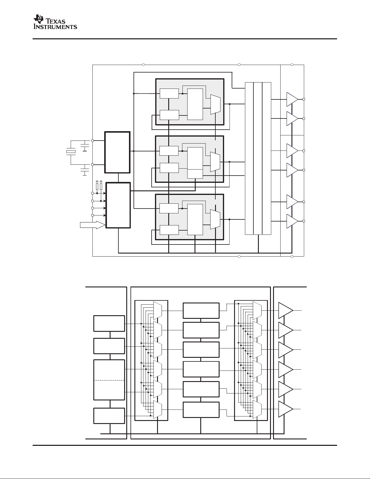
TERMINAL ASSIGNMENT
DESCRIPTION
The CDCE906 is one of the smallest and powerful
PLL synthesizer / multiplier / divider available today.
Despite its small physical outlines, the CDCE906 is
flexible. It has the capability to produce an almost
independent output frequency from a given input
frequency.
The input frequency can be derived from a LVCMOS,
differential input clock, or a single crystal. The
appropriate input waveform can be selected via the
SMBus data interface controller.
1
2 Pro-Clock is a trademark of Texas Instruments.
PRODUCTION DATA information is current as of publication date.
Products conform to specifications per the terms of the Texas
Instruments standard warranty. Production processing does not
necessarily include testing of all parameters.
Please be aware that an important notice concerning availability, standard warranty, and use in critical applications of
Texas Instruments semiconductor products and disclaimers thereto appears at the end of this data sheet.
Copyright © 2005 – 2007, Texas Instruments Incorporated
Page 2

www.ti.com
CDCE906
SCAS814H – NOVEMBER 2005 – REVISED DECEMBER 2007
DESCRIPTION (CONTINUED)
To achieve an independent output frequency the reference divider M and the feedback divider N for each PLL
can be set to values from 1 up to 511 for the M-Divider and from 1 up to 4095 for the N-Divider. The PLL-VCO
(voltage controlled oscillator) frequency than is routed to the free programmable output switching matrix to any of
the six outputs. The switching matrix includes an additional 7-bit post-divider (1-to-127) and an inverting logic for
each output.
The deep M/N divider ratio allows the generation of zero ppm clocks from any reference input frequency (e.g., a
27 MHz).
The CDCE906 includes three PLLs of those one supports SSC (spread-spectrum clocking). PLL1, PLL2, and
PLL3 are designed for frequencies up to 167 MHz and optimized for zero-ppm applications with wide divider
factors.
PLL2 also supports center-spread and down-spread spectrum clocking (SSC). This is a common technique to
reduce electro-magnetic interference. Also, the slew-rate controllable (SRC) output edges minimize EMI noise.
Based on the PLL frequency and the divider settings, the internal loop filter components will be automatically
adjusted to achieve high stability and optimized jitter transfer characteristic of the PLL.
The device supports non-volatile EEPROM programming for easy-customized application. It is preprogrammed
with a factory default configuration (see Figure 13 ) and can be reprogrammed to a different application
configuration before it goes onto the PCB or reprogrammed by in-system programming. A different device setting
is programmed via the serial SMBus interface.
Two free programmable inputs, S0 and S1, can be used to control for each application the most demanding logic
control settings (outputs disable to low, outputs 3-state, power down, PLL bypass, etc).
The CDCE906 has three power supply pins, V
operates from a single 3.3-V supply voltage. V
V
CCOUT1
supplies the outputs Y0 and Y1 and V
supplies can be 2.3 V to 3.6 V. At output voltages lower than 3.3 V, the output drive current is limited.
The CDCE906 is characterized for operation from 0 ° C to 70 ° C.
, V
CC
CCOUT1
CCOUT1
CCOUT2
and V
and V
CCOUT2
. V
CCOUT2
is the power supply for the device. It
CC
are the power supply pins for the outputs.
supplies the outputs Y2, Y3, Y4, and Y5. Both outputs
2 Submit Documentation Feedback Copyright © 2005 – 2007, Texas Instruments Incorporated
Product Folder Link(s): CDCE906
Page 3
www.ti.com
PLL1
XO
or
2LVCMOS
or
Differential
Input
MUX
MUX
PLL3
PFD
Filter
VCO
PLL2
w/SSC
PFD
Filter
VCO
SO/AO/CLK_SEL
S1/A1
SCLOCK
OutputSwitchMatrix
LV
CMOS
LV
CMOS
LV
CMOS
LV
CMOS
LV
CMOS
LV
CMOS
EEPROM
LOGIC
SMBUS
LOGIC
PFD
Filter
VCO
SDATA
Y5
Y4
Y3
Y2
Y1
Y0
VCO1Bypass
VCO2Bypass
VCO3Bypass
MUX
6xProgrammable7-BitDividerP0,P1,P2,P3,P4,P5,andInversionLogic
5x6ProgrammableSwitch A
PLL Bypass
V
CC
GND V
CCOUT1
GND V
CCOUT2
prg. 9Bit
DividerM
prg.12Bit
DividerN
prg.9Bit
DividerM
prg.12Bit
DividerN
prg.9Bit
DividerM
prg.12Bit
DividerN
Crystalor
ClockInput
CLK_IN1
FactoryPrg.
CLK_IN0
SSC
On/Off
6x6ProgrammableSwitchB
5x6 − Switch A
Input CLK
(PLL Bypass)
PLL 1
PLL 2
non SSC
PLL 2
w/ SSC
PLL 3
6x6 − Switch B7-Bit Divider
Y0
Y1
Y2
Y3
Y4
Y5
P0
P1
P2
P3
P4
P5
Programming
FUNCTIONAL BLOCK DIAGRAM
CDCE906
SCAS814H – NOVEMBER 2005 – REVISED DECEMBER 2007
OUTPUT SWITCH MATRIX
Copyright © 2005 – 2007, Texas Instruments Incorporated Submit Documentation Feedback 3
Product Folder Link(s): CDCE906
Page 4
www.ti.com
CDCE906
SCAS814H – NOVEMBER 2005 – REVISED DECEMBER 2007
TERMINAL FUNCTIONS
TERMINAL
NAME
Y0 to Y5 O LVCMOS outputs
TSSOP20
NO.
11, 12, 15,
16, 19, 20
CLK_IN0 5 I
CLK_IN1 6 I/O
V
CC
V
CCOUT1
V
CCOUT2
3, 7 Power 3.3-V power supply for the device.
14 Power Power supply for outputs Y0, Y1.
18 Power Power supply for outputs Y2, Y3, Y4, Y5.
GND 4, 8, 13, 17 Ground Ground
S0, A0,
CLK_SEL
1 I CLK_SEL (selects one of two LVCMOS clock inputs), dependent on the SMBus settings; LVCMOS
S1, A1 2 I
SDATA 9 I/O Serial control data input/output for SMBus controller; LVCMOS input
SCLOCK 10 I Serial control clock input for SMBus controller; LVCMOS input
I/O DESCRIPTION
Dependent on SMBus settings, CLK_IN0 is the crystal oscillator input and can also be used as
LVCMOS input or as positive differential signal inputs.
Dependent on SMBus settings, CLK_IN1 is serving as the crystal oscillator output or can be the
second LVCMOS input or the negative differential signal input.
User programmable control input S0 (PLL bypass or power-down mode) or AO (address bit 0), or
inputs; internal pullup 150 k Ω .
User programmable control input S1 (output enable/disable or all output low), A1 (address bit 1),
dependent on the SMBus settings; LVCMOS inputs; internal pullup 150 k Ω
ABSOLUTE MAXIMUM RATINGS
over operating free-air temperature range (unless otherwise noted)
V
V
V
I
I
I
O
T
stg
T
J
(1) Stresses beyond those listed under absolute maximum ratings may cause permanent damage to the device. These are stress ratings
(2) The input and output negative voltage ratings may be exceeded if the input and output clamp-current ratings are observed.
Supply voltage range – 0.5 to 4.6 V
CC
Input voltage range
I
Output voltage range
O
(2)
(2)
Input current (VI< 0, VI> VCC) ± 20 mA
Continuous output current ± 50 mA
Storage temperature range – 65 to 150 ° C
Maximum junction temperature 125 ° C
only and functional operation of the device at these or any other conditions beyond those indicated under recommended operating
conditions is not implied. Exposure to absolute maximum rated conditions for extended periods may affect device reliability.
(1)
VALUE UNIT
– 0.5 to V
– 0.5 to V
+ 0.5 V
CC
+ 0.5 V
CC
PACKAGE THERMAL RESISTANCE
for TSSOP20 (PW) Package
θ
JA
θ
JC
(1) The package thermal impedance is calculated in accordance with JESD 51 and JEDEC2S2P (high-k board).
Thermal resistance junction-to-ambient
Thermal resistance junction-to-case 19.7
(1)
PARAMETER AIRFLOW (LFM) ° C/W
0 66.3
150 59.3
250 56.3
500 51.9
4 Submit Documentation Feedback Copyright © 2005 – 2007, Texas Instruments Incorporated
Product Folder Link(s): CDCE906
Page 5
www.ti.com
SCAS814H – NOVEMBER 2005 – REVISED DECEMBER 2007
RECOMMENDED OPERATING CONDITIONS
over operating free-air temperature range (unless otherwise noted)
MIN NOM MAX UNIT
V
CC
V
CCOUT1
V
CCOUT2
V
IL
V
IH
V
Ithresh
V
I
|V
| Differential input voltage 0.1 V
ID
V
IC
IOH/ I
IOH/ I
C
L
T
A
(1) The minimum output voltage can be down to 1.8 V. See the application note for more information.
Device supply voltage 3 3.3 3.6 V
(1)
Output Y0,Y1 supply voltage 2.3 3.6 V
(1)
Output Y2, Y3, Y4, Y5 supply voltage 2.3 3.6 V
Low level input voltage LVCMOS 0.3 V
High level input voltage LVCMOS 0.7 V
Input voltage threshold LVCMOS 0.5 V
CC
CC
Input voltage range LVCMOS 0 3.6 V
Common-mode for differential input voltage 0.2 Vcc- 0.6 V
Output current (3.3 V) ± 6 mA
OL
Output current (2.5 V) ± 4 mA
OL
Output load LVCMOS 25 pF
Operating free-air temperature 0 70 ° C
RECOMMENDED CRYSTAL SPECIFICATIONS
MIN NOM MAX UNIT
f
Xtal
ESR Effective series resistance
C
(1) For crystal frequencies above 50 MHz the effective series resistor should not exceed 50 Ω to assure stable start-up condition.
(2) Maximum Power Handling (Drive Level) see Figure 16 .
Crystal input frequency range (fundamental mode) 8 27 54 MHz
(1) (2)
Input capacitance CLK_IN0 and CLK_IN1 3 pF
IN
15 60 Ω
CDCE906
CC
V
V
V
EEPROM SPECIFICATION
MIN TYP MAX UNIT
EEcyc Programming cycles of EEPROM 100 1000 Cycles
EEret Data retention 10 Years
TIMING REQUIREMENTS
over recommended ranges of supply voltage, load, and operating-free air temperature
MIN NOM MAX UNIT
CLK_IN REQUIREMENTS
f
CLK_IN
tr/ t
f
duty
REF
CLK_IN clock input frequency (LVCMOS or Differential) MHz
Rise and fall time CLK_IN signal (20% to 80%) 4 ns
Duty cycle CLK_IN at V
/ 2 40% 60%
CC
SMBus TIMING REQUIREMENTS (see Figure 11 )
f
SCLK
t
h(START)
t
w(SCLL)
t
w(SCLH)
t
su(START)
t
h(SDATA)
t
su(SDATA)
t
r
t
f
SCLK frequency 100 kHz
START hold time 4 µ s
SCLK low-pulse duration 4.7 µ s
SCLK high-pulse duration 4 50 µ s
START setup time 0.6 µ s
SDATA hold time 0.3 µ s
SDATA setup time 0.25 µ s
SCLK / SDATA input rise time 1000 ns
SCLK / SDATA input fall time 300 ns
PLL mode 1 167
PLL bypass mode 0 167
Copyright © 2005 – 2007, Texas Instruments Incorporated Submit Documentation Feedback 5
Product Folder Link(s): CDCE906
Page 6
www.ti.com
CDCE906
SCAS814H – NOVEMBER 2005 – REVISED DECEMBER 2007
TIMING REQUIREMENTS (continued)
over recommended ranges of supply voltage, load, and operating-free air temperature
MIN NOM MAX UNIT
t
su(STOP)
t
BUS
t
POR
DEVICE CHARACTERISTICS
over recommended operating free-air temperature range and test load (unless otherwise noted), see Figure 1
OVERALL PARAMETER
I
CC
I
CCPD
V
PUC
f
VCO
f
OUT
LVCMOS PARAMETER
V
IK
I
I
I
IH
I
IL
C
I
LVCMOS PARAMETER FOR V
V
OH
V
OL
t
,
PLH
t
PHL
tr0/t
f0
tr1/t
f1
tr2/t
f2
tr3/t
f3
STOP setup time 4 µ s
Bus free time 4.7 µ s
Time in which the device must be operational after power-on reset 500 ms
PARAMETER TEST CONDITIONS MIN TYP
Supply current
(2)
Power down current. Every circuit
powered down except SMBus
All PLLs on, all outputs on,
f
= 80 MHz, f
out
f
= 160 MHz
vco
fIN= 0 MHz, V
CLK_IN
= 3.6 V 50 µ A
CC
= 27 MHz, 90 115 mA
Supply voltage Vccthreshold for
power up control circuit
VCO frequency of internal PLL (any
of three PLLs)
Normal
speed-mode
(3)
High-speed mode
LVCMOS output frequency range
LVCMOS input voltage V
LVCMOS input current (CLK_IN0 /
CLK_IN1)
LVCMOS input current (For S1/S0) VI= VCC, V
LVCMOS input current (For S1/S0) VI= 0 V, V
Input capacitance at CLK_IN0 and VI= 0 V or V
CLK_IN1
ccout
LVCMOS high-level output voltage V
LVCMOS low-level output voltage V
Propagation delay ns
Rise and fall time for output slew
rate 0
Rise and fall time for output slew
rate 1
Rise and fall time for output slew
rate 2
Rise and fall time for output slew
rate 3 (Default Configuration)
(4)
V
= 2.5 V or 3.3 V 167 MHz
CC
= 3 V, II= – 18 mA – 1.2 V
CC
VI= 0 V or VCC, V
= 3.6 V 5 µ A
CC
= 3.6 V -35 -10 µ A
CC
CC
= 3.3-V Mode
V
= 3 V, IOH= – 0.1 mA 2.9
ccout
= 3 V, IOH= – 4 mA 2.4 V
ccout
V
= 3 V, IOH= – 6 mA 2.1
ccout
V
= 3 V, IOL= 0.1 mA 0.1
ccout
= 3 V, IOL= 4 mA 0.5 V
ccout
V
= 3 V, IOL= 6 mA 0.85
ccout
All PLL bypass 9
VCO bypass 11
V
= 3.3 V (20% – 80%) 1.7 3.3 4.8 ns
ccout
V
= 3.3 V (20% – 80%) 1.5 2.5 3.2 ns
ccout
V
= 3.3 V (20% – 80%) 1.2 1.6 2.1 ns
ccout
V
= 3.3 V (20% – 80%) 0.4 0.6 1 ns
ccout
All PLLs 80 200
PLL2 with SSC 80 167 MHz
(3)
= 3.6 V ± 5 µ A
CC
180 300
(1)
MAX UNIT
2.1 V
3 pF
(1) All typical values are at respective nominal VCC.
(2) For calculating total supply current, add the current from Figure 2 , Figure 3 , and Figure 4 . Using high-speed mode of the VCO reduces
the current consumption significantly. See Figure 3
(3) Normal-speed mode or high-speed mode must be selected by the VCO frequency selection bit in Byte 6, Bit [7:5]. The min f
lower but impacts jitter-performance.
(4) The maximum output frequency may be exceeded, but specifications under the Recommended Operating Condition may change and
are no longer assured. Do not exceed the maximum power dissipation of the 20-pin TSSOP package (600 mW at no air flow).
6 Submit Documentation Feedback Copyright © 2005 – 2007, Texas Instruments Incorporated
Product Folder Link(s): CDCE906
can be
VCO
Page 7
www.ti.com
SCAS814H – NOVEMBER 2005 – REVISED DECEMBER 2007
DEVICE CHARACTERISTICS (continued)
over recommended operating free-air temperature range and test load (unless otherwise noted), see Figure 1
PARAMETER TEST CONDITIONS MIN TYP
t
jit(cc)
t
jit(per)
t
sk(o)
Cycle-to-cycle jitter
Peak-to-peak period jitter
Output skew (see
odc Output duty cycle
LVCMOS PARAMETER FOR V
V
OH
V
OL
t
PLH
t
PHL
tr0/t
tr1/t
tr2/t
tr3/t
t
jit(cc)
t
jit(per)
t
sk(o)
LVCMOS high-level output voltage V
LVCMOS low-level output voltage V
,
Propagation delay ns
Rise and fall time for output
f0
slew rate 0
Rise and fall time for output
f1
slew rate 1
Rise and fall time for output
f2
slew rate 2
Rise and fall time for output
f3
slew rate 3 (Default Configuration)
Cycle-to-cycle jitter
Peak-to-peak period jitter
Output skew (see
odc Output duty cycle
(5) (6)
1 PLL, 1 Output f
3 PLLs, 3 Outputs f
(5) (6)
1 PLL, 1 Output f
3 PLLs, 3 Outputs f
(7)
and Table 5 ) 1.6-ns rise/fall time at
(8)
= 2.5-V Mode
ccout
f
= 150 MHz, Pdiv = 3
vco
f
= 100 MHz, Pdiv = 1 45% 55%
vco
(9)
V
= 2.3 V, IOH= 0.1 mA 2.2
ccout
= 2.3 V, IOH= – 3 mA 1.7 V
ccout
V
= 2.3 V, IOH= – 4 mA 1.5
ccout
V
= 2.3 V, IOL= 0.1 mA 0.1
ccout
= 2.3 V, IOL= 3 mA 0.5 V
ccout
V
= 2.3 V, IOL= 4 mA 0.85
ccout
All PLL bypass 9
VCO bypass 11
V
= 2.5 V (20% – 80%) 2 3.9 5.6 ns
ccout
V
= 2.5 V (20% – 80%) 1.8 2.9 4.4 ns
ccout
V
= 2.5 V (20% – 80%) 1.3 2 3.2 ns
ccout
V
= 2.5 V (20% – 80%) 0.4 0.8 1.1 ns
ccout
(10) (11)
1 PLL, 1 Output f
3 PLLs, 3 Outputs f
(10) (11)
1 PLL, 1 Output f
3 PLLs, 3 Outputs f
(12)
and Table 5 ) 250 ps
(13)
2-ns rise/fall time at
f
= 150 MHz, Pdiv = 3
VCO
f
= 100 MHz, Pdiv = 1 45% 55%
VCO
= 24.576 MHz 65 95
OUT
= 24.576 MHz 85 135
OUT
= 24.576 MHz 90 115
OUT
= 24.576 MHz 100 150
OUT
= 24.576 MHz 85 120
OUT
= 24.576 MHz 95 155
OUT
= 24.576 MHz 110 135
OUT
= 24.576 MHz 110 175
OUT
SMBus PARAMETER
V
IK
I
I
V
IH
V
IL
V
OL
C
C
SCLK and SDATA input clamp
voltage
SCLK and SDATA input current VI= 0 V or VCC, V
V
= 3 V, II= – 18 mA – 1.2 V
CC
= 3.6 V ± 5 µ A
CC
SCLK input high voltage 2.1 V
SCLK input low voltage 0.8 V
SDATA low-level output voltage IOL= 4 mA, V
Input capacitance at SCLK VI= 0 V or V
ISCLK
Input capacitance at SDATA VI= 0 V or V
ISDATA
= 3 V 0.4 V
CC
CC
CC
(5) 50000 cycles.
(6) Jitter depends on configuration. Jitter data is for normal tr/tf, input frequency = 27 MHz, f
(7) The t
(8) odc depends on output rise and fall time (tr/tf); above limits are for normal tr/tf.
specification is only valid for equal loading of all outputs.
sk(o)
= 147 MHz output.
VCO
(9) There is a limited drive capability at output supply voltage of 2.5 V. For proper termination, see application report SCAA080 .
(10) 50000 cycles.
(11) Jitter depends on configuration. Jitter data is for normal tr/tf, input frequency = 27 MHz, f
(12) The t
(13) odc depends on output rise and fall time (tr/tf); above limits are for normal tr/tf.
specification is only valid for equal loading of all outputs.
sk(o)
= 147 MHz output.
VCO
(1)
3 10 pF
3 10 pF
CDCE906
MAX UNIT
ps
ps
200 ps
ps
ps
Copyright © 2005 – 2007, Texas Instruments Incorporated Submit Documentation Feedback 7
Product Folder Link(s): CDCE906
Page 8
www.ti.com
Yn
1 kW
1 kW
10 pF
LVCMOS
CDCE906
PLL 1+PLL 2SSC+PLL3
V =3.3V,
Mdiv=1,
Ndiv=2,
P div=1,
VCOnormal-speedmode
CC
PLL 1+PLL 2+PLL3
PLL 1+PLL 2
f -[MHz]
VCO
210
I -[mA]
CC
PLL 1
20017016015090
90
80
80
0
0
70
70
60
60
50
50
40
40
30
30
20
20
10
10
140130120
120
110
110
100
100
190180
CDCE906
SCAS814H – NOVEMBER 2005 – REVISED DECEMBER 2007
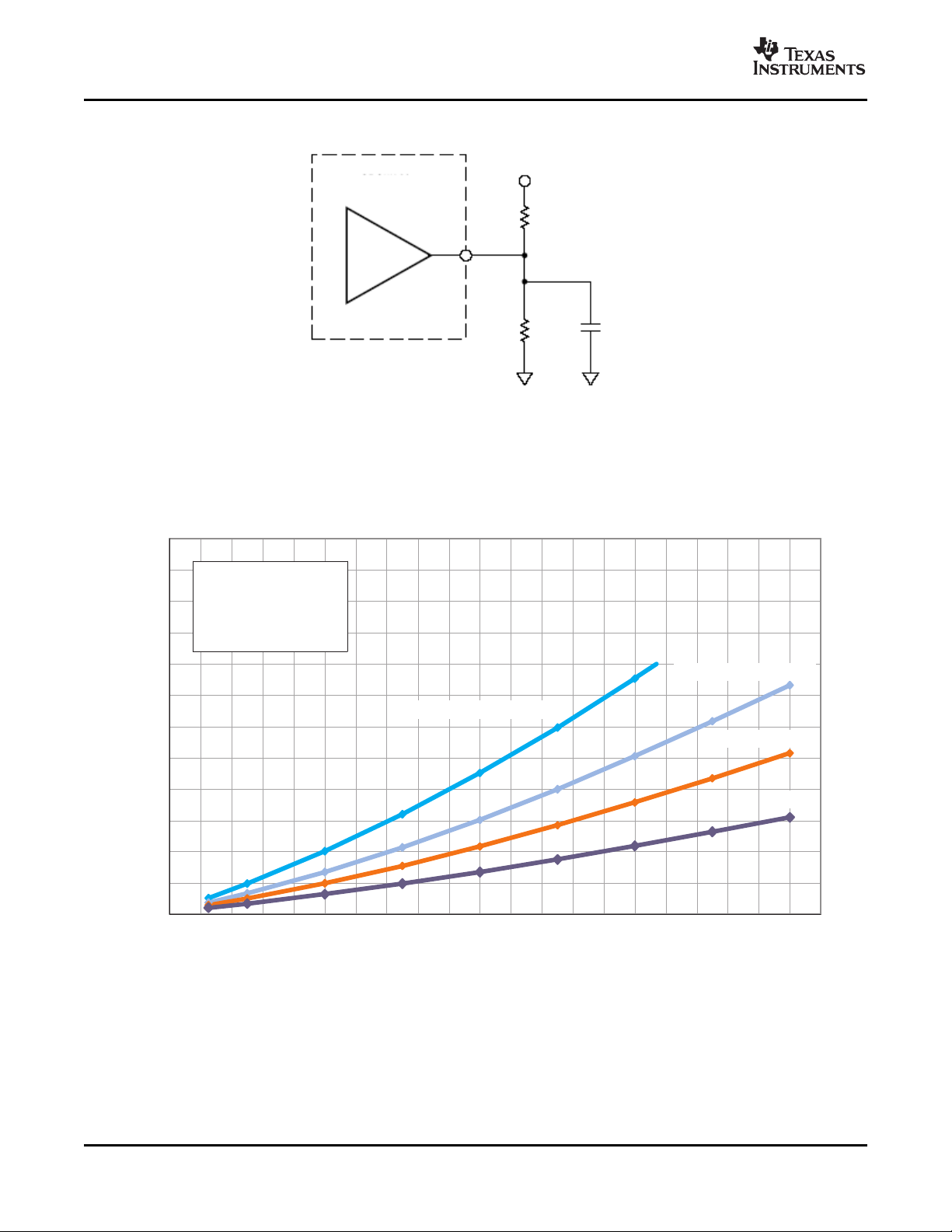
PARAMETER MEASUREMENT INFORMATION
Figure 1. Test Load
Figure 2. ICCvs Number of PLLs and VCO Frequency (VCO at Normal-Speed Mode, Byte 6 Bit [7:5])
TYPICAL CHARACTERISTICS
8 Submit Documentation Feedback Copyright © 2005 – 2007, Texas Instruments Incorporated
Product Folder Link(s): CDCE906
Page 9
www.ti.com
PLL 1+PLL 2SSC+PLL3
V =3.3V,
Mdiv=1,
Ndiv=2,
P div=1,
VCOhigh-speedmode
CC
PLL 1+PLL 2+PLL3
PLL 1+PLL 2
f -[MHz]
VCO
310
I
-[mA]
CC
PLL 1
300250190180
90
80
0
70
60
50
40
30
20
10
170160150
120
140
110
130
100
270260240230200 220210 290280
0
5
10
15
20
25
30
35
40
45
50
55
0 10 20 30 40 50 60 70 80 90 100 110 120 130 140 150 160 170 180
6Outputs
5Outputs
4Outputs
3Outputs
2Outputs
1Outputs
V =3.3V,
Mdiv=1,
Ndiv=2,
P div=1
CC
f -[MHz]
VCO
I -[mA]
CC
TYPICAL CHARACTERISTICS (continued)
CDCE906
SCAS814H – NOVEMBER 2005 – REVISED DECEMBER 2007
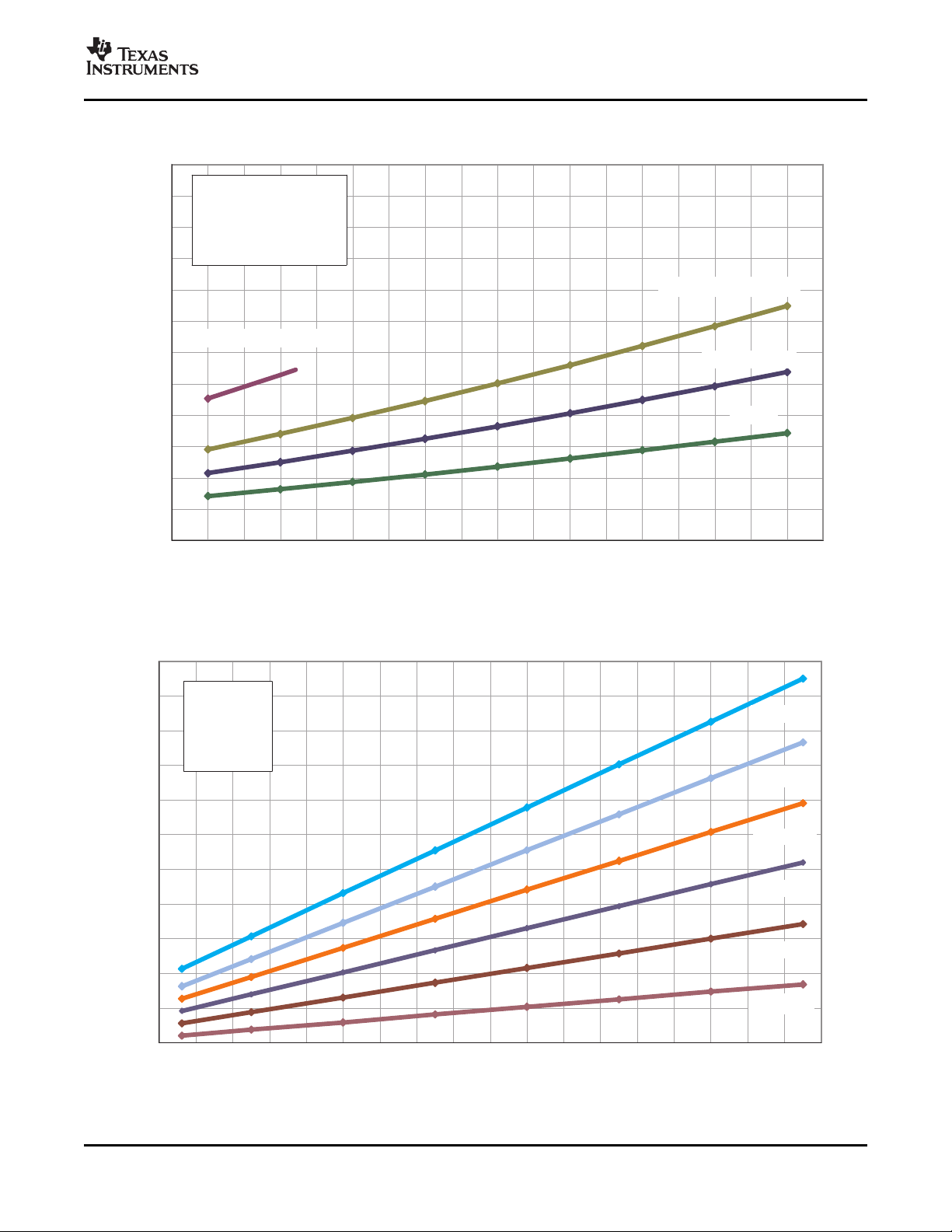
Figure 3. ICCvs Number of PLLs and VCO Frequency (VCO at High-Speed Mode, Byte 6 Bit [7:5])
Figure 4. I
vs Number of Outputs and VCO Frequency
CCOUT
Copyright © 2005 – 2007, Texas Instruments Incorporated Submit Documentation Feedback 9
Product Folder Link(s): CDCE906
Page 10

www.ti.com
0.0
0.2
0.4
0.6
0.8
1.0
1.2
1.4
1.6
1.8
2.0
2.2
2.4
2.6
2.8
3.0
3.2
3.4
3.6
90 100 110 120 130 140 150 160 170 180 190 200 210 220
VOHatV =3.6V
CCOUT
VOHatV =2.3V
CCOUT
VOLatV =3.6V
CCOUT
VOLatV =2.3V
CCOUT
f -[MHz]
OUT
VOUT-[V]
V =3.3V,
Mdiv=4,
Ndiv=15,
P div=1
CC
CDCE906
SCAS814H – NOVEMBER 2005 – REVISED DECEMBER 2007
TYPICAL CHARACTERISTICS (continued)
Figure 5. Output Swing vs Output Frequency
10 Submit Documentation Feedback Copyright © 2005 – 2007, Texas Instruments Incorporated
Product Folder Link(s): CDCE906
Page 11
www.ti.com
CDCE906
SCAS814H – NOVEMBER 2005 – REVISED DECEMBER 2007
APPLICATION INFORMATION
SMBus Data Interface
To enhance the flexibility and function of the clock synthesizer, a two-signal serial interface is provided. It follows
the SMBus specification Version 2.0, which is based upon the principals of operation of I2C. More details of the
SMBus specification can be found at http://www.smbus.org .
Through the SMBus, various device functions, such as individual clock output buffers, can be individually
enabled or disabled. The registers associated with the SMBus data interface initialize to their default setting upon
power-up, and therefore using this interface is optional. The clock device register changes are normally made
upon system initialization, if any are required.
Data Protocol
The clock driver serial protocol accepts Byte Write, Byte Read, Block Write, and Block Read operations from the
controller.
For Block Write/Read operations, the bytes must be accessed in sequential order from lowest to highest byte
(most significant bit first) with the ability to stop after any complete byte has been transferred. For Byte Write and
Byte Read operations, the system controller can access individually addressed bytes.
Once a byte has been sent, it will be written into the internal register and effective immediately. With the rising
edge of the ACK bit, this applies to each transferred byte, independent of whether this is a Byte Write or a Block
Write sequence.
If the EEPROM write cycle is initiated, the data of the internal SMBus register is written into the EEPROM.
During EEPROM write, no data is allowed to be sent to the device via the SMBus until the programming
sequence is completed. Data, however, can be readout during the programming sequence (byte read or block
read). The programming status can be monitored by EEPIP, byte 24 bit 7.
The offset of the indexed byte is encoded in the command code, as described in Table 1 .
The Block Write and Block Read protocol is outlined in Figure 9 and Figure 10 , while Figure 7 and Figure 8
outlines the corresponding Byte Write and Byte Read protocol.
Slave Receiver Address (7 bits)
A6 A5 A4 A3 A2 A1* A0* R/W
1 1 0 1 0 0 1 0
* Address bits A0 and A1 are programmable by the Configuration Inputs S0 and S1 (Byte 10 Bit [1:0] and Bit [3:2]. This allows addressing up
to four devices connected to the same SMBus.
Table 1. Command Code Definition
Bit Description
7
(6:0) Byte Offset for Read and Write operation.
0 = Block Read or Block Write operation
1 = Byte Read or Byte Write operation
Copyright © 2005 – 2007, Texas Instruments Incorporated Submit Documentation Feedback 11
Product Folder Link(s): CDCE906
Page 12
www.ti.com
1 7 1 1 8 1 1
S Slave Address Wr A Data Byte A P
S Start Condition
Sr
Reapeated Start Condition
Rd
Read (Bit Value = 1)
Wr
Write (Bit Value = 0)
A Acknowledge (ACK = 0 and NACK = 1)
P Stop Condition
PE Packet Error
Master to Slave Transmission
Slave to Master Transmission
CDCE906
SCAS814H – NOVEMBER 2005 – REVISED DECEMBER 2007
Figure 6. Generic Programming Sequence
Byte Write Programming Sequence
1 7 1 1 8 1 8 1 1
S Slave Address Wr A CommandCode A Data Byte A P
Figure 7. Byte Write Protocol
Byte Read Programming Sequence
1 7 1 1 8 1 1 7 1 1
S Slave Address Wr A CommandCode A S Slave Address Rd A
8 1 1
Data Byte A P
Figure 8. Byte Read Protocol
Block Write Programming Sequence
1 7 1 1 8 1 8 1
S Slave Address Wr A CommandCode A Byte Count N A
8 1 8 1 8 1 1
Data Byte 0 A Data Byte 1 A - - - - - Data Byte N – 1 A P
(1)
Data Byte 0 is reserved for revision code and vendor identification. However, this byte is used for internal test. Do not write into it other
than 0000 0001.
(1)
Figure 9. Block Write Protocol
12 Submit Documentation Feedback Copyright © 2005 – 2007, Texas Instruments Incorporated
Product Folder Link(s): CDCE906
Page 13
www.ti.com
P S P
SCLK
SDATA
A
Bit 7 (MSB)
Bit 6 Bit 0 (LSB)
t
h(SDATA)
t
su(SDATA)
t
su(START)
t
(BUS)
t
h(START)
t
r(SM)
t
r(SM)
t
f(SM)
t
f(SM)
t
W(SCLH)
t
W(SCLL)
t
su(STOP)
V
IH(SM)
V
IL(SM)
V
IH(SM)
V
IL(SM)
9
10
SDATA
SCLK
SMB Host
CDCE906
C
BUS
C
BUS
R
P
R
P
SCAS814H – NOVEMBER 2005 – REVISED DECEMBER 2007
Block Read Programming Sequence
1 7 1 1 8 1 1 7 1 1
S Slave Address Wr A CommandCode A Sr Slave Address Rd A
8 1 8 1 8 1 1
Byte Count N A Data Byte 0 A - - - - - Data Byte N – 1 A P
Figure 10. Block Read Protocol
CDCE906
Figure 11. Timing Diagram Serial Control Interface
SMBus Hardware Interface
The following diagram shows how the CDCE906 clock synthesizer is connected to the SMBus. Note that the
current through the pullup resistors (R
CDCE906 is not connected to the SMBus, then SDATA and SCLK inputs have to be connected with 10-k Ω
pullup resistors to V
to avoid floating input conditions.
CC
) must meet the SMBus specifications (min 100 µ A, max 350 µ A). If the
p
Figure 12. SMBus Hardware Interface
Copyright © 2005 – 2007, Texas Instruments Incorporated Submit Documentation Feedback 13
Product Folder Link(s): CDCE906
Page 14

www.ti.com
CDCE906
SCAS814H – NOVEMBER 2005 – REVISED DECEMBER 2007
Table 2. Register Configuration Command Bitmap
Adr Bit 7 Bit 6 Bit 5 Bit 4 Bit 3 Bit 2 Bit 1 Bit 0
Byte 0 Revision Code Vendor Identification
Byte 1 PLL1 Reference Divider M 9-Bit [7:0]
Byte 2 PLL1 Feedback Divider N 12-Bit [7:0]
Byte 3 PLL1 Mux PLL2 Mux PLL3 Mux PLL1 Feedback Divider N 12-Bit [11:8] PLL1 Ref
Byte 4 PLL2 Reference Divider M 9-Bit [7:0]
Byte 5 PLL2 Feedback Divider N 12-Bit [7:0]
Byte 6 PLL1 fvco PLL2 fvco PLL3 fvco PLL2 Feedback Divider N 12-Bit [11:8] PLL2 Ref
Selection Selection Selection Dev M [8]
Byte 7 PLL3 Reference Divider 9-Bit M [7:0]
Byte 8 PLL3 Feedback Divider N [12-Bit 7:0]
Byte 9 PLL Selection for P0 (Switch A) PLL3 Feedback Divider N 12-Bit [11:8] PLL3 Ref
Byte 10 PLL Selection for P1 (Switch A) Inp. Clock Configuration Inputs S1 Configuration Inputs S0
Selection
Byte 11 Input Signal Source PLL Selection for P3 (Switch A) PLL Selection for P2 (Switch A)
Byte 12 Reserved Power Down PLL Selection for P5 (Switch A) PLL Selection for P4 (Switch A)
Byte 13 Reserved 7-Bit Divider P0 [6:0]
Byte 14 Reserved 7-Bit Divider P1 [6:0]
Byte 15 Reserved 7-Bit Divider P2 [6:0]
Byte 16 Reserved 7-Bit Divider P3 [6:0]
Byte 17 Reserved 7-Bit Divider P4 [6:0]
Byte 18 Reserved 7-Bit Divider P5 [6:0]
Byte 19 Reserved Y0 Inv. or Y0 Slew-Rate Control Y0 Enable or Y0 Divider Selection (Switch B)
Non-Inv Low
Byte 20 Reserved Y1 Inv. or Y1 Slew-Rate Control Y1 Enable or Y1 Divider Selection (Switch B)
Non-Inv Low
Byte 21 Reserved Y2 Inv. or Y2 Slew-Rate Control Y2 Enable or Y2 Divider Selection (Switch B)
Non-Inv Low
Byte 22 Reserved Y3 Inv. or Y3 Slew-Rate Control Y3 Enable or Y3 Divider Selection (Switch B)
Non-Inv Low
Byte 23 Reserved Y4 Inv. or Y4 Slew-Rate Control Y4 Enable or Y4 Divider Selection (Switch B)
Non-Inv Low
Byte 24 EEPIP [read Y5 Inv or Y5 Slew-Rate Control Y5 Enable or Y5 Divider Selection (Switch B)
only] Non-Inv Low
Byte 25 EELOCK Spread Spectrum (SSC) Modulation Frequency Selection for SSC
Selection
Byte 26 EEWRITE 7-Bit Byte Count
Dev M [8]
Dev M [8]
Default Device Setting
The internal EEPROM of CDCE906 is pre-programmed with a factory default configuration as shown below. This
puts the device in an operating mode without the need to program it first. The default setting appears after power
is switched on or after a power-down/up sequence until it is re-programmed by the user to a different application
configuration. A new register setting is programmed via the serial SMBUS Interface.
A different default setting can be programmed upon customer request. Contact a Texas Instruments sales or
marketing representative for more information.
14 Submit Documentation Feedback Copyright © 2005 – 2007, Texas Instruments Incorporated
Product Folder Link(s): CDCE906
Page 15

www.ti.com
PLL1
XO
or
2LVCMOS
or
Differential
Input
MUX
MUX
DividerM
1
MUX
DividerM
375
PLL3
PFD
Filter
VCO
PLL2
w/SSC
PFD
Filter
VCO
DividerN
8
DividerN
250
DividerN
3136
SO/CLK_SEL
S1
SCLOCK
OutputSwitchMatrix
27MHz
PROGRAMMING
LOGIC
SMBUS
LOGIC
PFD
Filter
VCO
SDATA
P0-Div
10
P1-Div
20
P2-Div
8
P3-Div
9
P4-Div
32
P5-Div
4
f
VCO3
=225.792MHz
CLK_IN0
CLK_IN1
27MHz
Crystal
1
4pF
1
4pF
SSC-OFF
Y5
Y4
Y3
Y2
Y1
Y0
27MHz
27MHz
27MHz
27MHz
LV
CMOS
LV
CMOS
LV
CMOS
LV
CMOS
LV
CMOS
LV
CMOS
27MHz
DividerM
27
f
VCO1
=216MHz
f
VCO2
=250MHz
fout=
finxN
MxP
, i.e.fout=
27MHzx8
(1x8)
=27MHz
CDCE906
SCAS814H – NOVEMBER 2005 – REVISED DECEMBER 2007
NOTE: All outputs are enabled and in non-inverting mode. S0, S1, and SSC comply according the default setting described in
The output frequency can be calculated:
Byte 10 and Byte 25 respectively.
Figure 13. Default Device Setting
(1)
Copyright © 2005 – 2007, Texas Instruments Incorporated Submit Documentation Feedback 15
Product Folder Link(s): CDCE906
Page 16

www.ti.com
CDCE906
SCAS814H – NOVEMBER 2005 – REVISED DECEMBER 2007
Functional Description of the Logic
All Bytes are read-/write-able, unless otherwise expressly mentioned.
Byte 0 (read only): Vendor Identification Bits [3:0]; Revision Code Bit [7:4]
Revision Code
X X X X 0 0 0 1
(1) Byte 0 is readable by "Byte Read sequency" only.
Byte 1 to 9: Reference Divider M of PLL1, PLL2, PLL3
M8 M7 M6 M5 M4 M3 M2 M1 M0 Div by Default
0 0 0 0 0 0 0 0 0 Not allowed
0 0 0 0 0 0 0 0 1 1
0 0 0 0 0 0 0 1 0 2
0 0 0 0 0 0 0 1 1 3
1 1 1 1 1 1 1 0 1 509
1 1 1 1 1 1 1 1 0 510
1 1 1 1 1 1 1 1 1 511
(1) By selecting the PLL divider factors, M ≤ N and 80 MHz ≤ fvco ≤ 300 MHz.
(2) Unless customer specific setting.
(3) Default setting of divider M for PLL1 = 1, for PLL2 = 27 and for PLL3 = 375.
Byte 1 to 9: Feedback Divider N of PLL1, PLL2, PLL3
N11 N10 N9 N8 N7 N6 N5 N4 N3 N2 N1 N0 Div by Default
0 0 0 0 0 0 0 0 0 0 0 0
0 0 0 0 0 0 0 0 0 0 0 1 1
0 0 0 0 0 0 0 0 0 0 1 0 2
0 0 0 0 0 0 0 0 0 0 1 1 3
1 1 1 1 1 1 1 1 1 1 0 1 4093
1 1 1 1 1 1 1 1 1 1 1 0 4094
1 1 1 1 1 1 1 1 1 1 1 1 4095
(1) By selecting the PLL divider factors, M ≤ N and 80 MHz ≤ fvco ≤ 300 MHz.
(2) Unless customer specific setting.
(3) Default setting of divider N for PLL1 = 8, for PLL2 = 250 and for PLL3 = 3136.
Byte 3 Bit [7:5]: PLL (VCO) Bypass Multiplexer
PLLxMUX PLL (VCO) MUX Output Default
0 PLLx Yes
1 VCO bypass
(1) Unless customer specific setting.
Byte 6 Bit [7:5]: VCO Frequency Selection Mode for each PLL
PLLxFVCO VCO Frequency Range Default
0 80-200 MHz
1 180-300 MHz Yes
(1) This bit selects the normal-speed mode or the high-speed mode for the dedicated VCO in PLL1, PLL2 or PLL3. At power-up, the
high-speed mode is selected, f
(2) Unless customer specific setting.
(1)
(1)
•
•
•
(1)
is 180-300 MHz. In case of higher f
VCO
Vendor Identification
Not
allowed
•
•
•
(1)
(1)
(2)
, this bit has to be set to [1].
VCO
(2) (3)
(2) (3)
16 Submit Documentation Feedback Copyright © 2005 – 2007, Texas Instruments Incorporated
Product Folder Link(s): CDCE906
Page 17

www.ti.com
CDCE906
SCAS814H – NOVEMBER 2005 – REVISED DECEMBER 2007
Byte 9 to 12: Outputs Switch Matrix (5x6 Switch A) PLL Selection for P-Divider P0-P5
SWAPx2 SWAPx1 SWAPx0 Any Output Px Default
0 0 0 PLL bypass (input clock)
0 0 1 PLL1 P2, P3, P4, P5
0 1 0 PLL2 non-SSC P0
0 1 1 PLL2 w/ SSC
1 0 0 PLL3 P1
1 0 1 Reserved
1 1 0 Reserved
1 1 1 Reserved
(1) Unless customer specific setting.
(2) PLL2 has a SSC output and non-SSC output. If SSC bypass is selected (see Byte 25, Bit [6:4]), the SSC circuitry of PLL2 is
powered-down and the SSC output is reset to logic low. The non-SSC output of PLL2 is not affected by this mode and can still be used.
Byte 10, Bit [1:0]: Configuration Settings of Input S0/A0/CLK_SEL
S01 S00 Function Default
0 0
If S0 is low, the PLLs and the clock-input stage are going into power-down mode, outputs are in Yes
3-state, all actual register settings will be maintained, SMBus stays active
If S0 is low, the PLL and all dividers (M-Div and P-Div) are bypassed and PLL is in power-down,
0 1 all outputs are active (inv. or non-inv.), actual register settings will be maintained, SMBus stays
active; this mode is useful for production test;
CLK_SEL (input clock selection — overwrites the CLK_SEL setting in Byte 10, Bit [4])
1 0 — CLK_SEL is set low selects CLK_IN_IN0
— CLK_SEL is set high selects CLK_IN_IN1
1 1
In this mode, the control input S0 is interpreted as address bit A0 of the slave receiver address
(4)
byte
(1) Unless customer specific setting.
(2) Power-down mode overwrites 3-state or low-state of S1 setting in Byte 10, Bit [3:2].
(3) If the clock input (CLK_IN0/CLK_IN1) is selected as crystal input or differential clock input (Byte 11, Bit [7:6]) then this setting is not
relevant.
(4) To use this pin as Slave Receiver Address Bit A0, an Initialization pattern needs to be sent to CDCE906. When S00/S01 is set to be 1,
the S0 input pin will be interpreted in the next read or write cycle as the Address Bit A0 of the Slave Receiver Address Byte. Note that
right after the Byte 10 (S00/S01) has been written, A0 (via S0-pin) will immediately be active (also when Byte 10 is sent within a block
write sequence). After the Initialization each CDCE906 has its own S0 dependent Slave Receiver Address and can be addressed
accordingly to their new valid address.
Byte 10, Bit [3:2]: Configuration Settings of Input S1/A1
S11 S10 Function Default
0 0 If S1 is set low, all outputs are switched to a low-state (non-inv.) or high-state (inv.); Yes
0 1 If S1 is set low, all outputs are switched to a 3-state
1 0 Reserved
1 1
In this mode, the control input S1 is interpreted as Address Bit A1 of the Slave Receiver Address
(2)
Byte
(1) Unless customer specific setting.
(2) To use this pin as Slave Receiver Address Bit A1, an Initialization pattern needs to be sent to CDCE906. When S10/S11 is set to be 1,
the S1 input pin will be interpreted in the next read or write cycle as the Address Bit A1 of the Slave Receiver Address Byte. Note that
right after the Byte 10 (S10/S11) has been written, A1 (via S1-pin) will immediately be active (also when Byte 10 is sent within a block
write sequence). After the Initialization each CDCE906 has its own S1 dependent Slave Receiver Address and can be addressed
accordingly to their new valid address.
Byte 10, Bit [4]: Input Clock Selection
(1)
CLKSEL Input Clock Default
0 CLK_IN0 Yes
1 CLK_IN1
(1) This bit is not relevant, if crystal input or differential clock input is selected, Byte 11, Bit [7:6].
(2) Unless customer specific setting.
(2)
(2)
(3)
(2)
(1)
(1)
(1)
Copyright © 2005 – 2007, Texas Instruments Incorporated Submit Documentation Feedback 17
Product Folder Link(s): CDCE906
Page 18
www.ti.com
CDCE906
SCAS814H – NOVEMBER 2005 – REVISED DECEMBER 2007
Byte 11, Bit [7:6]: Input Signal Source
(1)
IS1 IS0 Function Default
0 0 CLK_IN0 is Crystal Oscillator Input and CLK_IN1 is serving as Crystal Oscillator Output. Yes
0 1
CLK_IN0 and CLK_IN1 are two LVCMOS Inputs. CLK_IN0 or CLK_IN1 are selectable via
CLK_SEL control pin.
1 0 CLK_IN0 and CLK_IN1 serve as differential signal inputs.
1 1 Reserved
(1) In case the crystal input or differential clock input is selected, the input clock selection, Byte 10, Bit [4], is not relevant.
(2) Unless customer specific setting.
Byte 12, Bit [6]: Power-Down Mode (except SMBus)
PD Power-Down Mode Default
0 Normal Device Operation Yes
1 Power Down
(2)
(1) Unless customer specific setting.
(2) In power down, all PLLs and the Clock-Input-Stage are going into power-down mode, all outputs are in 3-State, all actual register
settings will be maintained and SMBus stays active. Power-Down Mode overwrites 3-State or Low-State of S0 and S1 setting in Byte 10.
Byte 13 to 18, Bit [6:0]: Outputs Switch Matrix - 6x7-Bit Divider P0-P5
DIVYx6 DIVYx5 DIVYx4 DIVYx3 DIVYx2 DIVYx1 DIVYx0 Div by Default
0 0 0 0 0 0 0 Not allowed
0 0 0 0 0 0 1 1
0 0 0 0 0 1 0 2
•
•
•
1 1 1 1 1 0 1 125
1 1 1 1 1 1 0 126
1 1 1 1 1 1 1 127
(1) Unless customer specific setting.
(2) Default setting of divider P0 = 10, P1 = 20, P2 = 8, P3 = 9, P4 = 32, and P5 = 4
Byte 19 to 24, Bit [5:4]: LVCMOS Output Rise/Fall Time Setting at Y0-Y5
SRCYx1 SRCYx0 Yx Default
0 0 Nominal +3 ns (tr0/tf0)
0 1 Nominal +2 ns (tr1/tf1)
1 0 Nominal +1 ns (tr2/tf2)
1 1 Nominal (tr3/tf3) Yes
(1) Unless customer specific setting.
Byte 19 to 24, Bit [2:0]: Outputs Switch Matrix (6 x 6 Switch B) Divider (P0-P5) Selection for Outputs Y0-Y5
SWBYx2 SWBYx1 SWBYx0 Any Output Yx Default
0 0 0 Divider P0
0 0 1 Divider P1
0 1 0 Divider P2 Y0, Y1, Y2, Y3, Y4, Y5
0 1 1 Divider P3
1 0 0 Divider P4
1 0 1 Divider P5
1 1 0 Reserved
1 1 1 Reserved
(1) Unless customer specific setting.
(2)
(1)
(1) (2)
(1)
(1)
18 Submit Documentation Feedback Copyright © 2005 – 2007, Texas Instruments Incorporated
Product Folder Link(s): CDCE906
Page 19

www.ti.com
CDCE906
SCAS814H – NOVEMBER 2005 – REVISED DECEMBER 2007
Byte 19 to 24, Bit [3]: Output Y0-Y5 Enable or Low-State
ENDISYx Output Yx Default
0 Disable to low
1 Enable Yes
(1) Unless customer specific setting.
Byte 19 to 24, Bit [6]: Output Y0-Y5 Non-Inverting/Inverting
INVYx Output Yx Status Default
0 Non-inverting Yes
1 Inverting
(1) Unless customer specific setting.
Byte 24, Bit [7] (read only): EEPROM Programming In Process Status
(1)
EEPIP Indicate EEPROM Write Process Default
0 No programming
1 Programming in process
(1) This read only Bit indicates an EEPROM write process. It is set to high if programming starts and resets to low if programming is
completed. Any data written to the EEPIP-Bit will be ignored. During programming, no data are allowed to be sent to the device via the
SMBus until the programming sequence is completed. Data, however, can be readout during the programming sequence (Byte Read or
Block Read).
Byte 25, Bit [3:0]: SSC Modulation Frequency Selection in the Range of 30 kHz 60 kHz
FSSC3 FSSC2 FSSC1 FSSC0 Modulation f
0 0 0 0 5680 f
0 0 0 1 5412 18.5 20.3 22.2 24.0 25.9 27.7 29.6 30.9
0 0 1 0 5144 19.4 21.4 23.3 25.3 27.2 29.2 31.1 32.5
0 0 1 1 4876 20.5 22.6 24.6 26.7 28.7 30.8 32.8 34.2
0 1 0 0 4608 21.7 23.9 26.0 28.2 30.4 32.6 34.7 36.2
0 1 0 1 4340 23.0 25.3 27.6 30.0 32.3 34.6 36.9 38.5
0 1 1 0 4072 24.6 27.0 29.5 31.9 34.4 36.8 39.3 41.0
0 1 1 1 3804 26.3 28.9 31.5 34.2 36.8 39.4 42.1 43.9
1 0 0 0 3536 28.3 31.1 33.9 36.8 39.6 42.4 45.2 47.2
1 0 0 1 3286 30.4 33.5 36.5 39.6 42.6 45.6 48.7 50.8 Yes
1 0 1 0 3000 33.3 36.7 40.0 43.3 46.7 50.0 53.3 55.7
1 0 1 1 2732 36.6 40.3 43.9 47.6 51.2 54.9 58.6 61.1
1 1 0 0 2464 40.6 44.6 48.7 52.8 56.8 60.9 64.9 67.8
1 1 0 1 2196 45.5 50.1 54.6 59.2 63.8 68.3 72.9 76.0
1 1 1 0 1928 51.9 57.1 62.2 67.4 72.6 77.8 83.0 86.6
1 1 1 1 1660 60.2 66.3 72.3 78.3 84.3 90.4 96.4 100.6
Factor
mod
[kHz]
100 110 120 130 140 150 160 167
17.6 19.4 21.1 22.9 24.6 26.4 28.2 29.4
(1)
[MHz] Default
vco
(1) The PLL has to be bypassed (turned off) when changing SSC Modulation Frequency Factor on-the-fly. This can be done by following
programming sequence: bypass PLL2 (Byte 3, Bit 6 = 1); write new Modulation Factor (Byte 25); re-activate PLL2 (Byte 3, Bit 6 = 0).
(2) Unless customer specific setting.
(1)
(1)
(2)
Copyright © 2005 – 2007, Texas Instruments Incorporated Submit Documentation Feedback 19
Product Folder Link(s): CDCE906
Page 20

www.ti.com
CDCE906
SCAS814H – NOVEMBER 2005 – REVISED DECEMBER 2007
Byte 25, Bit [6:4]: SSC Modulation Amount
(1)
SSC2 SSC1 SSC0 Function Default
0 0 0 SSC Modulation Amount 0% = SSC bypass for PLL
(3)
Yes
0 0 1 SSC Modulation Amount ± 0.1% (center spread)
0 1 0 SSC Modulation Amount ± 0.25% (center spread)
0 1 1 SSC Modulation Amount ± 0.4% (center spread)
1 0 0 SSC Modulation Amount 1% (down spread)
1 0 1 SSC Modulation Amount 1.5% (down spread)
1 1 0 SSC Modulation Amount 2% (down spread)
1 1 1 SSC Modulation Amount 3% (down spread)
(1) The PLL has to be bypassed (turned off) when changing SSC Modulation Amount on-the-fly. This can be done by following
programming sequence: bypass PLL2 (Byte 3, Bit 6 = 1); write new Modulation Amount (Byte 25); re-activate PLL2 (Byte 3, Bit 6 = 0).
(2) Unless customer specific setting.
(3) If SSC bypass is selected, SSC circuitry of PLL2 is powered-down and the SSC output is reset to logic low. The non-SSC output of
PLL2 is not affected by this mode and can still be used.
Byte 25, Bit [7]: Permanently Lock EEPROM-Data
EELOCK Permanently Lock EEPROM
(1)
(2)
Default
0 No Yes
1 Yes
(1) If this bit is set, the actual data in the EEPROM will be permanently locked. There is no further programming possible, even this bit is set
low. Data, however can still be written via SMBUS to the internal register to change device function on the fly. But new data no longer
can be stored into the EEPROM.
(2) Unless customer specific setting.
Byte 26, Bit [6:0]: Byte Count
(1)
BC6 BC5 BC4 BC3 BC2 BC1 BC0 No. of Bytes Default
0 0 0 0 0 0 0 Not allowed
0 0 0 0 0 0 1 1
0 0 0 0 0 1 0 2
0 0 0 0 0 1 1 3
•
•
•
0 0 1 1 0 1 1 27 Yes
•
•
•
1 1 1 1 1 0 1 125
1 1 1 1 1 1 0 126
1 1 1 1 1 1 1 127
(1) Defines the number of Bytes, which will be sent from this device at the next Block Read protocol.
(2) Unless customer specific setting.
Byte 26, Bit [7]: Initiate EEPROM Write Cycle
EEWRITE Starts EEPROM Write Cycle Default
(1)
(2)
0 No Yes
1 Yes
(1) The EEPROM WRITE cycle is initiated with the rising edge of the EEWRITE-Bit. A static level high does not trigger an EEPROM WRITE
cycle. This bit stays high until the user reset it to low (it will not automatically be reset after the programming has been completed).
Therefore, to initiate an EEPROM WRITE cycle, it is recommended to send a zero-one sequence to the EEWRITE bit in Byte 26.
During EEPROM programming, no data are allowed to be sent to the device via the SMBus until the programming sequence has been
completed. Data, however, can be readout during the programming sequence (Byte Read or Block Read). The programming status can
be monitored by readout EEPIP, Byte 24 – Bit 7. If EELOCK is set, no EEPROM programming will be possible.
(2) Unless customer specific setting.
(2)
(2)
20 Submit Documentation Feedback Copyright © 2005 – 2007, Texas Instruments Incorporated
Product Folder Link(s): CDCE906
Page 21

www.ti.com
CDCE906
SCAS814H – NOVEMBER 2005 – REVISED DECEMBER 2007
FUNCTIONAL DESCRIPTION
Zero ppm Audio and Video System Clock Generation and Divider Setting
The CDCE906 is ideally suited for audio and video applications. It consists of a triple PLL clock generator which
generates up to six audio, video and system clocks from i.e. a 27-MHz master clock. The output frequencies are
programmable to meet different application requirements. The master clock can be either a crystal oscillator or
an external input clock signal. The CDCE906 provides a very low jitter, high accuracy clock with zero ppm for the
common audio and video clocks. The following table shows the system clocks versus the standard sampling
frequency and the corresponding divider settings.
Audio Rate fs x 256 fs x 384
[kHz] [MHz] [MHz]
16 4.096 375 2048 36 0 6.144 125 768 27 0
22.05 5.6448 75 392 25 0 8.4672 125 588 15 0
24 6.144 125 768 27 0 9.216 125 768 18 0
32 8.192 375 2048 18 0 12.288 375 2048 12 0
44.1 11.2896 375 1568 10 0 16.9344 125 784 10 0
48 12.288 375 2048 12 0 18.432 125 768 9 0
96 24.576 375 2048 6 0 36.864 375 2048 4 0
Divider Divider
M N P M N P
Error ppm Error ppm
Audio Rate fs x 512 fs x 768
[kHz] [MHz] [MHz]
16 8.192 375 2048 18 0 12.288 375 2048 12 0
22.05 11.2896 375 1568 10 0 16.9344 125 784 10 0
24 12.288 375 2048 12 0 18.432 125 768 9 0
32 16.384 375 2048 9 0 24.576 375 2048 6 0
44.1 22.5792 375 1568 5 0 33.8688 125 784 5 0
48 24.576 375 2048 6 0 36.864 375 2048 4 0
96 49.152 375 2048 3 0 73.728 375 2048 2 0
Divider Divider
M N P M N P
Error ppm Error ppm
NOTE: Input frequency is 27 MHz.
Video Divider Divider Divider
Rate
[MHz]
27 54 1 8 4 0 27 - - 1 0 13.5 - - 2 0
2 Error 1 Error 0.5 Error
[MHz] ppm [MHz] ppm [MHz] ppm
M N P M N P M N P
Copyright © 2005 – 2007, Texas Instruments Incorporated Submit Documentation Feedback 21
Product Folder Link(s): CDCE906
Page 22

www.ti.com
27 MHz
Crystal
CDCE906
16.9344 MHz (384fs)
33.8688 MHz (768fs)
11.2896 MHz (256fs)
27 MHz
DVD−DSP
MPEG/AC−3
Audio Dec
Karaoke
DSP
PCM1716
Front
Surround
Center
Subwoofer
CPU Clock
64 MHz
i.e. audio rate: 44.1 kHz
XO
or
2LVCMOS
or
Differential
Input
CLK_IN0
CLK_IN1
Input source select
(from EEPROM)
C
X0
C
X1
crystal
unit
C
ICB
C
ICB
CDCE906
SCAS814H – NOVEMBER 2005 – REVISED DECEMBER 2007
Typical applications for the CDCE906 are digital HDTV systems, gaming consoles, DVD players, DVD add-on
cards for multimedia PCs, and step-top boxes.
Figure 14. CDCE906 System Application Block Diagram
Clock Inputs (CLK_IN0 and CLK_IN1)
The CDCE906 features two clock inputs which can be used as:
• Crystal oscillator input (default setting)
• Two independent single-ended LVCMOS inputs
• Differential signal input
The dedicated clock input can be selected by the input signal source Bit [7:6] of Byte 11.
Crystal Oscillator Inputs
The input frequency range in crystal mode is 8 MHz to 54 MHz. The CDCE906 uses a Pierce-type oscillator
circuitry with included feedback resistance for the inverting amplifier. The user, however, has to add external
capacitors C
, C
X0
) to match the input load capacitor from the crystal (see Figure 15 ). The required values can
X1
be calculated:
C
= C
where C
X0
= 2 × CL– C
X1
is the crystal load capacitor as specified for the crystal unit and C
L
,
ICB
is the input capacitance of the
ICB
device including the board capacitance (stray capacitance of PCB).
For example, for a fundamental 27-MHz crystal with C
C
= C
X0
= (2 × 9 pF) – 3 pF = 15 pF.
X1
of 9 pF and C
L
of 4 pF,
ICB
It is important to use a short PCB trace from the device to the crystal unit to keep the stray capacitance of the
oscillator loop to a minimum.
22 Submit Documentation Feedback Copyright © 2005 – 2007, Texas Instruments Incorporated
Figure 15. Crystal Input Circuitry
Product Folder Link(s): CDCE906
Page 23

www.ti.com
0
10
20
30
40
50
60
70
80
90
100
5 10 15 20 25 30 35 40 45 50 55
C=18pF
Upk=300mV
Frequency − MHz
P
drive
− W
21 W
ESR=60
ESR=50
ESR=40
ESR=30
ESR=25
ESR=15
XO
or
2LVCMOS
or
Differential
input
CLK_IN0
CLK_IN1
CLK_SEL
(A)
Input Source Select
(From EEPROM)
CDCE906
SCAS814H – NOVEMBER 2005 – REVISED DECEMBER 2007
In order to ensure a stable oscillating, a certain drive power must be applied. The CDCE906 features an input
oscillator with adaptive gain control which relieves the user to manually program the gain. The drive level is the
amount of power dissipated by the oscillating crystal unit and is usually specified in terms of power dissipated by
the resonator (equivalent series resistance (ESR)). Figure 16 gives the resulting drive level vs crystal frequency
and ESR.
Figure 16. Crystal Drive Power
For example, if a 27-MHz crystal with ESR of 50 Ω is used and 2 × C
is 18 pF, the drive power is 21 µ W. Drive
L
level should be held to a minimum to avoid over driving the crystal. The maximum power dissipation is specified
for each type of crystal in the oscillator specifications, i.e., 100 µ W for the example above.
Single-Ended LVCMOS Clock Inputs
When selecting the LVCMOS clock mode, CLK_IN0 and CLK_IN1 act as regular clock inputs pins and can be
driven up to 167 MHz. Both clock inputs circuitry are equal in design and can be used independently to each
other (see Figure 17 ). The internal clock select bit, Byte 10, Bit [4], selects one of the two input clocks. CLK_IN0
is the default selection. There is also the option to program the external control pin S0/A0/CLK_SEL as clock
select pin, Byte 10, Bit [1:0].
The two clock inputs can be used for redundancy switching, i.e. to switch between a primary clock and
secondary clock. Note a phase difference between the clock inputs may require PLL correction. Also in case of
different frequencies between the primary and secondary clock, the PLL has to re-lock to the new frequency.
A. CLK_SEL is optional and can be configured by EEPROM setting.
Copyright © 2005 – 2007, Texas Instruments Incorporated Submit Documentation Feedback 23
Figure 17. LVCMOS Clock Input Circuitry
Product Folder Link(s): CDCE906
Page 24

www.ti.com
XO
or
2LVCMOS
or
Differential
input
CLK_IN0
CLK_IN1
Input source select
(from EEPROM)
MUX
9−Bit Divider M
1 .. 511
PLLx
12−Bit Divider N
1 .. 4095
PFD
Filter
VCO
SSC
(PLL2 only)
Input Clock
Programming
PLL output
SSC output
(PLL2 Only)
VCO Bypass
CDCE906
SCAS814H – NOVEMBER 2005 – REVISED DECEMBER 2007
Differential Clock Inputs
The CDCE906 supports differential signaling as well. In this mode, CLK_IN0 and CLK_IN1 pin serve as
differential signal inputs and can be driven up to 167 MHz.
The minimum magnitude of the differential input voltage is 100 mV over a differential common-mode input
voltage range of 200 mV to V
structure is recommended to adjust the different physical layers (see Figure 18 ). The capacitor removes the dc
component of the signal (common-mode voltage), while the ac component (voltage swing) is passed on. A
resistor pull-up and/or pull-down network represents the biasing structure used to set the common-mode voltage
on the receiver side of the ac-coupling capacitor. DC coupling is also possible.
– 0.6. If LVDS or LVPECL signal levels are applied, ac-coupling and a biasing
CC
Figure 18. Differential Clock Input Circuitry
PLL Configuration and Setting
The CDCE906 includes three PLLs which are equal in function and performance. Except PLL2 which in addition
supports spread spectrum clocking (SSC) generation. Figure 19 shows the block diagram of the PLL.
Figure 19. PLL Architecture
All three PLLs are designed for easiest configuration. The user just has to define the input and output
frequencies or the divider (M, N, P) setting respectively. All other parameters, such as charge-pump current, filter
components, phase margin, or loop bandwidth are controlled and set by the device itself. This assures optimized
jitter attenuation and loop stability.
The PLL support normal-speed mode (80 MHz ≤ f
MHz) which can be selected by PLLxFVCO (Bit [7:5] of Byte 6). The respective speed option assures stable
operation and lowest jitter.
The divider M and divider N operates internally as fractional divider for f
divider ratio for zero ppm output clock error.
In case of f
For optimized jitter performance, keep divider M as small as possible. Also, the fractional divider concept
requires a PLL divider configuration, M ≤ N (or N/M ≥ 1).
24 Submit Documentation Feedback Copyright © 2005 – 2007, Texas Instruments Incorporated
VCO
> 250 MHz, it is recommended that integer factors of N/M are used only.
Product Folder Link(s): CDCE906
≤ 200 MHz) and high-speed mode (180 MHz ≤ f
VCO
up to 250 MHz. This allows fractional
VCO
≤ 300
VCO
Page 25

www.ti.com
Down Spread 3%
9thHarmonic, fm = 60 kHz
11.3dB
7dB
Center Spread+0.4%
9thHarmonic, fm = 60 kHz
Down Spread 3%
9thHarmonic, fm = 60
11.3dB11.3 dB
7dB7 dB
Center Spread+0.4%
9thHarmonic, fm = 60
CDCE906
SCAS814H – NOVEMBER 2005 – REVISED DECEMBER 2007
Additionally, each PLL supports two bypass options:
• PLL Bypass and
• VCO Bypass
In PLL bypass mode, the PLL completely is bypassed, so that the input clock is switched directly to the
Output-Switch-A (SWAPxx of Byte 9 to12). In the VCO bypass mode, only the VCO of the respective PLL is
bypassed by setting PLLxMUX to 1 (Bit [7:5] of Byte 3). But the divider M still is useable and expands the output
divider by additional 9-bits. This gives a total divider range of M x P = 511 × 127 = 64897. In VCO bypass mode
the respective PLL block is powered down and minimizes current consumption.
Table 3. Example for Divide, Multiplication, and Bypass Operation
Function Equation
Fractional
Integer Factor
VCO bypass f
(1) P-divider of Output-Switch-Matrix is included in the calculation.
(2) Fractional operation for f
(3) Integer operation for f
(2)
(3)
f
= fINx (N/M)/P 30.72 155.52 155.52 16 81 1 5.0625 155.52
OUT
f
= fINx (N/M)/P 27 162 162 1 6 1 6 162
OUT
OUT
VCO
Spread Spectrum Clocking and EMI Reduction
In addition to the basic PLL function, PLL2 supports spread spectrum clocking (SSC) as well. Thus, PLL 2
features two outputs, a SSC output and a non-SSC output. Both outputs can be used in parallel. The mean
phase of the Center Spread SSC modulated signal is equal to the phase of the non-modulated input frequency.
SSC is selected by Output-Switch-A (SWAPxx of Byte 9 to 12).
SSC also is bypass-able (Byte 25, Bit [6:4]), which powers-down the SSC output and set it to logic low state. The
non-SSC output of PLL2 is not affected by this mode and can still be used.
SSC is an effective method to reduce electro-magnetic interference (EMI) noise in high-speed applications. It
reduces the RF energy peak of the clock signal by modulating the frequency and spread the energy of the signal
to a broader frequency range. Because the energy of the clock signal remains constant, a varying frequency that
broadens the overtones necessarily lowers their amplitudes. Figure 20 shows the effect of SSC on a 54-MHz
clock signal for DSP
(1)
= fIN/(M x P) 30.72 0.06 0.06 8 — 64 — —
≤ 250 MHz.
VCO
> 250 MHz.
f
IN
[MHz] [MHz] [MHz]
f
OUT-desired
f
OUT-actual
M N P N/M
Divider f
[MHz]
VCO
The peak amplitude of the modulated clock is 11.3 dB lower than the non-modulated carrier frequency for down
spread and radiated less electro-magnetic energy.
Copyright © 2005 – 2007, Texas Instruments Incorporated Submit Documentation Feedback 25
Figure 20. Spread Spectrum Clocking With Center Spread and Down Spread
Product Folder Link(s): CDCE906
Page 26

www.ti.com
3
4
5
6
7
8
9
10
11
12
30 40 50 60
3% Down Spread
2% Down Spread
fmodulation − kHz
EMI Reduction− dB
+0.4 Center Spread
+0.25 Center Spread
CDCE906
SCAS814H – NOVEMBER 2005 – REVISED DECEMBER 2007
In SSC mode, the user can select the SSC modulation amount and SSC modulation frequency. The modulation
amount is the frequency deviation based to the carrier (min/max frequency), whereas the modulation frequency
determines the speed of the frequency variation. In SSC mode, the maximum VCO frequency is limited to 167
MHz.
SSC Modulation Amount
The CDCE906 supports center spread modulation and down spread modulation. In center spread, the clock is
symmetrically shifted around the carrier frequency and can be ± 0.1%, ± 0.25%, and ± 0.4%. At down spread, the
clock frequency is always lower than the carrier frequency and can be 1%, 1.5%, 2%, and 3%. The down spread
is preferred if a system can not tolerate an operating frequency higher than the nominal frequency (over-clocking
problem).
Example:
Modulation Type Minimum Center Maximum
A ± 0.25% center spread 53.865 MHz 54 MHz 54.135 MHz
B 1% down spread 53.46 MHz — 54 MHz
C 0.5% down spread
(1) A down spread of 0.5% of a 54-MHz carrier is equivalent to 59.865 MHz at a center spread of ± 0.25%.
(1)
SSC Modulation Frequency
The modulation frequency (sweep rate) can be selected between 30 kHz and 60 kHz. It is also based on the
VCO frequency as shown in the SSC Modulation Frequency Selection as shown on page 19. As shown in
Figure 21 , the damping increases with higher modulation frequencies. It may be limited by the tracking skew of a
downstream PLL. The CDCE906 uses a triangle modulation profile which is one of the common profiles for SSC.
Frequency Frequency Frequency
53.73 MHz 53.865 MHz 54 MHz
Further EMI Reduction
The optimum damping is a combination of modulation amount, modulation frequency and the harmonics which
are considered. Note that higher order harmonic frequencies results in stronger EMI reduction because of
respective higher frequency deviation.
As seen in Figure 22 and Figure 23 , a slower output slew rate and/or smaller output signal amplitude helps to
reduce EMI emission even more. Both measures reduce the RF energy of clock harmonics. The CDCE906
allows slew rate control in four steps between 0.6 ns and 3.3 ns (Byte 19-24, Bit [5:4]). The output amplitude is
set by the two independent output supply voltage pins, V
Even a lower output supply voltage down to 1.8 V works, but the maximum frequency has to be considered.
26 Submit Documentation Feedback Copyright © 2005 – 2007, Texas Instruments Incorporated
Figure 21. EMI Reduction vs f
Product Folder Link(s): CDCE906
and V
and f
Amount
, and can vary from 2.3 V to 3.6 V.
CCOUT2
Modulation
CCOUT1
Page 27

www.ti.com
11.3dB
7dB
11.3dB11.3dB
7dB7dB
nom−1
nom
nom+2
−3dB
6.4dB
nom−1
nom
nom+2
−2.5dB
5.6dB
Slew-Rate for V
CCOUT
= 2.5 V Slew-Rate for V
CCOUT
= 3.3 V
−1
0
1
2
3
4
5
3.6 V3 V2.5 V
V
CCOUT
EMI Reduction − dB
(Relative to Nom)
CDCE906
SCAS814H – NOVEMBER 2005 – REVISED DECEMBER 2007
Figure 22. EMI Reduction vs Slew-Rate and V
Figure 23. EMI Reduction vs V
ccout
ccout
Multi-Function Control Inputs S0 and S1
The CDCE906 features two user definable inputs pins which can be used as external control pins or address
pins. When programmed as control pins, they can function as clock select pin, enable/disable pin or device
power-down pin. If both pins used as address-bits, up to four devices can be connected to the same SMBus. The
respective function is set in Byte 10; Bit [3:0]. Table 4 shows the possible setting for the different output
conditions, clock select and device addresses.
Copyright © 2005 – 2007, Texas Instruments Incorporated Submit Documentation Feedback 27
Product Folder Link(s): CDCE906
Page 28

www.ti.com
CDCE906
SCAS814H – NOVEMBER 2005 – REVISED DECEMBER 2007
Table 4. Configuration Setting of Control Inputs
Configuration Bits
Byte 10, Byte 10,
Bit [3:2] Bit [1:0]
S11 S10 S01 S00 S1 S0 Yx Outputs Power Pin 2 Pin 1
0 X 0 X 1 1 Active No Output ctrl Output ctrl
0 0 0 X 0 1 Low/High
0 1 0 X 0 1 3-State Outputs only Output ctrl Output ctrl
0 X 0 0 X 0 3-State PLL, inputs and outputs Output ctrl Output ctrl and pd
0 X 0 1 0 0 S10=0: low/high
0 X 0 1 1 0 Active PLL only Output ctrl PLL and Div bypass
0 X 1 0 0 0/1
0 X 1 0 1 0/1
1 1 1 1 X X Active No A1
(1) A non-inverting output will be set to low and an inverting output will be set to high.
(2) If S0 is 0, CLK_IN0 is selected; if S0 is 1, CLK_IN1 is selected.
(3) S0 and S1 are interpreted as Address Bit A0 and A1 of the Slave Receiver Address Byte.
External Control Pins Device Function
(Pin 2) (Pin 1) Down
(1)
(1)
S10=1: 3-State
(2)
(2)
S10=0: Low/High
S10=1: 3-State
Active No Output ctrl CLK_SEL
(1)
No Output ctrl Output ctrl
PLL only Output ctrl PLL and Div bypass
No Output ctrl CLK_SEL
(3)
(3)
A0
As shown in Table 4 , there is a specific order of the different output condition: Power-down mode overwrites
3-state, 3-state overwrites low-state, and low-state overwrites active-state.
Output Switching Matrix
The flexible architecture of the output switch matrix allows the user to switch any of the internal clock signal
sources via a free-selectable post-divider to any of the six outputs.
As shown in Figure 24 , the CDCE906 is based on two banks of switches and six post-dividers. Switch A
comprises six 5-Input-Muxes which selects one of the four PLL clock outputs or directly selects the input clock
and feed it to one of the 7-bit post-divider (P-Divider). Switch B is made up of six 6-Input-Muxes which takes any
post-divider and feeds it to one of the six outputs, Yx.
Switch B was added to the output switch matrix to ensure that outputs frequencies derive from one P-divider are
100% phase aligned. Also, the P-divider is built in a way that every divide factor is automatically duty-cycle
corrected. Changing the divider value on the fly may cause a glitch on the output.
28 Submit Documentation Feedback Copyright © 2005 – 2007, Texas Instruments Incorporated
Product Folder Link(s): CDCE906
Page 29

www.ti.com
5x6 − Switch A
Input CLK
(PLL Bypass)
PLL 1
PLL 2
non SSC
PLL 2
w/ SSC
PLL 3
6x6 − Switch B
7-Bit Divider
Y0
Y1
Y2
Y3
Y4
Y5
Output Switch Matrix
P0
(1..127)
P2
(1..127)
P3
(1..127)
P4
(1..127)
P5
(1..127)
Programming
OutputsInternal Clock Sources
PLL/Input_Clk
Selection
P-Divider
Selection
Output Selection:
Active/Low/3-State/
Inverting/Non-Inverting
P-Divider
Setting
P1
(1..127)
Slew Rate/V
CCOUT
Inverting
Slew Rate
Low Select
Enable/Disable
Clock
div by 3
Buffer
Sel
M
U
X
P−div(0) output
P−div(1) output
P−div(2) output
P−div(3) output
P−div(4) output
P−div(5) output
Yx
S1
Inversion Select
Slew-Rate Control
Low Select
Enable/Disable
P−Divider Select
(Optional all
outputs low
or 3−State)
V
CCOUT1/VCCOUT2
CDCE906
SCAS814H – NOVEMBER 2005 – REVISED DECEMBER 2007
Figure 24. CDCE906 Output Switch Matrix
In addition, the outputs can be switched active, low or 3-state and/or 180 degree phase shifted. Also the outputs
slew-rate and the output-voltage is user selectable.
LVCMOS Output Configuration
The output stage of the CDCE906 supports all common output setting, such as enable, disable, low-state and
signal inversion (180 degree phase shift). It further features slew-rate control (0.6 ns to 3.3 ns) and variable
output supply voltage (2.3 V to 3.6 V).
Figure 25. Block Diagram of Output Architecture Figure 26. Example for Output Waveforms
All output settings are programmable via SMBus:
• enable, disable, low-state via external control pins S0 and S1 → Byte 10, Bit[3:0]
• enable or disable-to-low → Byte 19 to 24, Bit[3]
• inverting/non-inverting → Byte 19 to 24, Bit[6]
• slew-rate control → Byte 19 to 24, Bit[5:4]
• output swing → external pins V
Copyright © 2005 – 2007, Texas Instruments Incorporated Submit Documentation Feedback 29
CCOUT1
(Pin 14) and V
Product Folder Link(s): CDCE906
CCOUT2
(Pin 18)
Page 30

www.ti.com
CDCE906
SCAS814H – NOVEMBER 2005 – REVISED DECEMBER 2007
Performance Data: Output Skew, Jitter, Cross Coupling, Noise Rejection (Spur-Suppression), and Phase Noise
Output Skew
Skew is an important parameter for clock distribution circuits. It is defined as the time difference between outputs
that are driven by the same input clock. Table 5 shows the output skew (t
and low-to-high transitions over the entire range of supply voltages, operating temperature and output voltage
swing.
Table 5. Output Skew
PARAMETER V
t
sk(o)
ccout
2.5 V 130 250 ps
3.3 V 130 200 ps
TYP MAX UNIT
Jitter Performance
Jitter is a major parameter for PLL-based clock driver circuits. This becomes important as speed increases and
timing budget decreases. The PLL and internal circuits of CDCE906 are designed for lowest jitter. The
peak-to-peak period jitter is only 60 ps (typical). Table 6 gives the peak-to-peak and rms deviation of
cycle-to-cycle jitter, period jitter and phase jitter as taken during characterization.
) of the CDCE906 for high-to-low
sk(o)
Table 6. Jitter Performance of CDCE906
PARAMETER f
t
jit(cc)
t
jit(per)
t
jit(phase)
(1) All typical and maximum values are at V
10000 cycles.
50 MHz 55 – 75 – ps
133 MHz 50 – 85 –
50 MHz 60 4 76 7 ps
133 MHz 55 5 84 11
50 MHz 730 90 840 115 ps
133 MHz 930 130 1310 175
out
= 3.3 V, temperature = 25 ° C, V
CC
(1)
TYP
Peak-Peak rms Peak-Peak rms
(one sigma) (one sigma)
= 3.3 V; one output is switching, data taken over several
ccout
(1)
MAX
UNIT
Figure 27 , Figure 28 , and Figure 29 show the relationship between cycle-to-cycle jitter, period jitter, and phase
jitter over 10000 samples. The jitter varies with a smaller or wider sample window. The cycle-to-cycle jitter and
period jitter show the measured value whereas the phase jitter is the accumulated period jitter.
Cycle-to-Cycle jitter (t
) is the variation in cycle time of a clock signal between adjacent cycles, over a random
jit(cc)
sample of adjacent cycle pairs. Cycle-to-cycle jitter will never be greater than the period jitter. It is also known as
adjacent cycle jitter.
30 Submit Documentation Feedback Copyright © 2005 – 2007, Texas Instruments Incorporated
Product Folder Link(s): CDCE906
Page 31

www.ti.com
−40
−30
−20
−10
0
10
20
30
40
1 1001 2001 3001 4001 5001 6001 7001 8001 9001 10001
Cycle
tjit(cc) [ps]
−25
−20
−15
−10
−5
0
5
10
15
20
25
1 1001 2001 3001 4001 5001 6001 7001 8001 9001 10001
Cycle
tjit(per) [ps]
CDCE906
SCAS814H – NOVEMBER 2005 – REVISED DECEMBER 2007
Figure 27. Snapshot of Cycle-to-Cycle Jitter
Period jitter (t
) is the deviation in cycle time of a clock signal with respect to the ideal period (1/fo) over a
jit(per)
random sample of cycles. In reference to a PLL, period jitter is the worst-case period deviation from the ideal that
would ever occur on the PLLs outputs. This is also referred to as short-term jitter.
Copyright © 2005 – 2007, Texas Instruments Incorporated Submit Documentation Feedback 31
Figure 28. Snapshot of Period Jitter
Product Folder Link(s): CDCE906
Page 32

www.ti.com
−300
−250
−200
−150
−100
−50
0
50
100
150
200
250
300
1 1001 2001 3001 4001 5001 6001 7001 8001 9001 10001
Cycle
tjit(phase) [ps]
CDCE906
SCAS814H – NOVEMBER 2005 – REVISED DECEMBER 2007
Phase jitter (t
) is the long-term variation of the clock signal. It is the cumulative deviation in t( Θ ) for a
jit(phase)
controlled edge with respect to a t( Θ ) mean in a random sample of cycles. Phase jitter, Time Interval Error (TIE),
or Wander are used in literature to describe long-term variation in frequency. As of ITU-T: G.810, wander is
defined as phase variation at rates less than 10 Hz while jitter is defined as phase variation greater than 10 Hz.
The measurement interval must be long enough to gain a meaningful result. Wander can be caused by
temperature drift, aging, supply voltage drift, etc.
Figure 29. Snapshot of Phase Jitter
Jitter also depends on the VCO frequency (f
compared to a lower f
. The VCO frequency can be defined via the M- and N-divider of the PLL.
VCO
) of the PLL. A higher f
VCO
VCO
results in better jitter performance
As the CDCE906 supports a pretty wide frequency range, the device offers a VCO Frequency Selection Bit, Bit
[7:5] of Byte 6. This bit defines the jitter-optimized frequency range of each PLL. The user can select between
the normal-speed mode (80 MHz to 200 MHz) and the high-speed mode (180 MHz to 300 MHz). Figure 30
shows the jitter performance over f
for the two frequency ranges.
VCO
32 Submit Documentation Feedback Copyright © 2005 – 2007, Texas Instruments Incorporated
Product Folder Link(s): CDCE906
Page 33

www.ti.com
0
20
40
60
80
100
120
140
160
180
200
220
240
260
280
300
0 20 40 60 80 100 120 140 160 180 200 220 240 260 280 300 320 340 360
T =25 C,
V =3.3V,
A
CC
o
Mdiv=4,
Ndiv=15,
P div=3
High-Speed Mode
>180MHz
f FrequencyRange
VCO
forHigh-SpeedMode
f
forNormal-SpeedMode
VCO
FrequencyRange
Normal-SpeedMode
<200MHz
f
VCO
− MHzSetPoint
t
jit(per)p-p
− ps
CDCE906
SCAS814H – NOVEMBER 2005 – REVISED DECEMBER 2007
Figure 30. Period Jitter vs f
for Normal-Speed Mode and High-Speed Mode
VCO
The TI Pro Clock software automatically calculates the PLL parameter for jitter-optimized performance.
Cross Coupling, Spur Suppression, and Noise Rejection
Cross-Coupling in ICs occurs through interactions between several parts of the chip such as between output
stages, metal lines, bond wires, substrate, etc. The coupling can be capacitive, inductive and resistive (ohmic)
induced by output switching, leakage current, ground bouncing, power supply transients, etc.
The CDCE906 is designed using the RFSiGe process technology. This process gives excellent performance in
linearity, low power consumption, best-in-class noise performance and good isolation characteristics between the
on-chip components.
The good isolation is a major benefit of the RFSiGe process because it minimizes the coupling effect. Even if all
three PLLs are active and all outputs are on, the noise suppression is well above 50 dB. Figure 31 and Figure 32
show an example of noise coupling, spur-suppression, and power supply noise rejection of CDCE906. Die
respective measurement conditions are shown in Figure 31 and Figure 32 .
Copyright © 2005 – 2007, Texas Instruments Incorporated Submit Documentation Feedback 33
Product Folder Link(s): CDCE906
Page 34

www.ti.com
carrier
48MHz
carrier
48MHz
spurs at
47MHz&49MHz
56 dB
carrier
48MHz
spurs at
47MHz&49MHz
56 dB
spur 47MHz and
fundamental at 1MHz
w Measured Y0: 48 MHz
w Y1, Y2, Y3, Y4 & Y5 tri−stated
w Inserted 30mV 1MHz @ Vcc = 3.3V
CDCE906
SCAS814H – NOVEMBER 2005 – REVISED DECEMBER 2007
Figure 31. Noise Coupling and Spur Suppression
Figure 32. Power Supply Noise Rejection
Phase Noise Characteristic
In high-speed communication systems, the phase noise characteristic of the PLL frequency synthesizer is of high
interest. Phase noise describes the stability of the clock signal in the frequency domain, similar to the jitter
specification in the time domain.
Phase noise is a result of random and discrete noise causing a broad slope and spurious peaks. The discrete
spurious components could be caused by known clock frequencies in the signal source, power line interference,
and mixer products. The broadening caused by random noise fluctuation is due to phase noise. It can be the
result of thermal noise, shot noise and/or flicker noise in active and passive devices.
Important factor for PLL synthesizer is the loop bandwidth ( – 3 dB cut-off frequency) — large loop bandwidth
(LBW) results in fast transient response but have less reference spur attenuation. The LBW of the CDCE906 is
about 100 kHz to 250 kHz, dependent on selected PLL parameter.
For the CDCE906, two phase noise characteristics are of interest: The phase noise of the crystal-input stage and
the phase noise of the internal PLL (VCO). The following Figure shows the respective phase noise characteristic.
34 Submit Documentation Feedback Copyright © 2005 – 2007, Texas Instruments Incorporated
Product Folder Link(s): CDCE906
Page 35

www.ti.com
dBc/Hz
−150
−140
−130
−120
−110
−100
−90
−80
−70
−60
−50
1.0E+01 1.0E+02 1.0E+03 1.0E+04 1.0E+05 1.0E+06 1.0E+07
CDCE906Cyrstal27MHzInput
27MHzBufferedOutput
CDCE906f
OUT
135MHz
f 135MHz
VCO
f
offset
-[Hz]
CDCE906f
OUT
135MHz
f 270MHz
VCO
PhaseNoiseComparison
f 135MHz
f 135MHzvs270MHz
OUT
VCO
CDCE906
SCAS814H – NOVEMBER 2005 – REVISED DECEMBER 2007
Figure 33. Phase Noise Characteristic
PLL Lock-Time
Some applications use frequency switching, i.e. to change frequency in TV application (switching between
channels) or change the PCI-X frequency in computers. The time spent by the PLL in achieving the new
frequency is of main interest. The lock time is the time it takes to jump from one specified frequency to another
specified frequency within a given frequency tolerance (Figure 34 ). It should be low, because a long lock time
impacts the data rate of the system.
The PLL Lock Time depends on the device configuration and can be changed by the VCO frequency, i.e. by
changing the M/N divider values. Table 7 gives the typical lock times of the CDCE906 and Figure 34 shows a
snapshot of a frequency switch.
Table 7. CDCE906 PLL Lock-Times
Description Lock Time (Typical) Unit
Frequency change via reprogramming of N/M counter 100 µ s
Frequency change via CLK_SEL pin (switching between CLK_IN0 and CLK_IN1) 100 µ s
Power-up lock time with system clock 50 µ s
Power-up lock time with 27-MHz Crystal at CLK_IN0 and CLK_IN1 300
(1) Is the result of crystal power up (200 µ s) and PLL Lock Time (100 µ s).
(1)
µ s
Copyright © 2005 – 2007, Texas Instruments Incorporated Submit Documentation Feedback 35
Product Folder Link(s): CDCE906
Page 36

www.ti.com
EVM Board Configuration:
•
Y0 (PLL1), Y1 3 state
•
CLK_IN: Crystal 27 MHz
•
measured Channel: Y0
Measurement:
•
Start Condition:ƒ(M = 10, N = 30) = 81 MHz
•
Byte 2 write: N = 30 (81 MHz) => N = 110 (297 MHz)
Result:
•60ms to PLL Pull In
•90ms to PLL Phase Lock
20ms/div
81
297
0
60
t [ms]
Start Condition:
Acknowledge of
N-Divider Byte
Frequency
Response
Curve of Y0
f (MHz)
V
t
Typ3.3V
Typ2.1V
Typ1.7V
A
B
C
D
V
CC
V
PUC_ON
V
PUC_OFF
GND
CDCE906
SCAS814H – NOVEMBER 2005 – REVISED DECEMBER 2007
Figure 34. Snapshot of the PLL Lock-Time
Power Supply Sequence
The CDCE906 includes the following three power supply pins: V
supply sequencing requirements, as the three power nodes are separated from each other. So, power can be
supplied in any order to the three nodes.
Also, the part has a power-up circuitry which switches the device on if V
device off at V
< 1.7 V (typ). In power-down mode, all outputs and clock inputs are switched off.
CC
, V
CC
, and V
CCOUT1
exceeds 2.1 V (typ) and switches the
CC
CCOUT2
. There are no power
Device Behavior during Supply Voltage Drops
The CDCE906 has a Power-Up-Circuit, which activates the device function at V
PUC_ON
same time, the EEPROM information is loaded into the register. This mechanism ensures that there is a
pre-defined default after Power-Up and no need to reprogram the CDCE906 in the application.
In the event of a supply-voltage-drop, the Power-Up-Circuit assures that there is always a defined setup within
the register. Figure 35 shows possible voltage drops with different amplitudes.
(typical 2.1 V). At the
36 Submit Documentation Feedback Copyright © 2005 – 2007, Texas Instruments Incorporated
Figure 35. Different Voltage Drops on V
Product Folder Link(s): CDCE906
During Operation
CC
Page 37

www.ti.com
CDCE906
SCAS814H – NOVEMBER 2005 – REVISED DECEMBER 2007
The CDCE906 Power-Up-Circuit has an inbuilt hysteresis. If the voltage stays above V
at 1.7 V, the register content stays unchanged. If the voltage drops below V
reloaded by the EEPROM after V
PUC_ON
is crossed again. V
PUC_ON
is typically 2.1 V. Table 8 show the content of
PUC_OFF
PUC_OFF
, which is typically
, the internal register is
the EEPROM and the Register after above voltage drops scenarios.
Table 8. EEPROM and Register Content After V
Power Drop EEPROM Content Register Content
A Unchanged Unchanged
B Unchanged Unchanged
C Unchanged Reloaded from EEPROM
D Unchanged Reloaded from EEPROM
Drop
CC
EVM and Programming SW
The CDCE906 EVM is a development kit consisting of a performance evaluation module, the TI Pro Clock
software, and the User's Guide. Contact Texas Instruments sales or marketing representative for more
information.
Copyright © 2005 – 2007, Texas Instruments Incorporated Submit Documentation Feedback 37
Product Folder Link(s): CDCE906
Page 38

PACKAGE OPTION ADDENDUM
www.ti.com
11-Dec-2007
PACKAGING INFORMATION
Orderable Device Status
(1)
Package
Type
Package
Drawing
Pins Package
Qty
Eco Plan
CDCE906PW ACTIVE TSSOP PW 20 70 Green (RoHS &
no Sb/Br)
CDCE906PWG4 ACTIVE TSSOP PW 20 70 Green (RoHS &
no Sb/Br)
CDCE906PWR ACTIVE TSSOP PW 20 2000 Green (RoHS &
no Sb/Br)
CDCE906PWRG4 ACTIVE TSSOP PW 20 2000 Green (RoHS &
no Sb/Br)
(1)
The marketing status values are defined as follows:
ACTIVE: Product device recommended for new designs.
LIFEBUY: TI has announced that the device will be discontinued, and a lifetime-buy period is in effect.
NRND: Not recommended for new designs. Device is in production to support existing customers, but TI does not recommend using this part in
a new design.
PREVIEW: Device has been announced but is not in production. Samples may or may not be available.
OBSOLETE: TI has discontinued the production of the device.
(2)
Eco Plan - The planned eco-friendly classification: Pb-Free (RoHS), Pb-Free (RoHS Exempt), or Green (RoHS & no Sb/Br) - please check
http://www.ti.com/productcontent for the latest availability information and additional product content details.
TBD: The Pb-Free/Green conversion plan has not been defined.
Pb-Free (RoHS): TI's terms "Lead-Free" or "Pb-Free" mean semiconductor products that are compatible with the current RoHS requirements
for all 6 substances, including the requirement that lead not exceed 0.1% by weight in homogeneous materials. Where designed to be soldered
at high temperatures, TI Pb-Free products are suitable for use in specified lead-free processes.
Pb-Free (RoHS Exempt): This component has a RoHS exemption for either 1) lead-based flip-chip solder bumps used between the die and
package, or 2) lead-based die adhesive used between the die and leadframe. The component is otherwise considered Pb-Free (RoHS
compatible) as defined above.
Green (RoHS & no Sb/Br): TI defines "Green" to mean Pb-Free (RoHS compatible), and free of Bromine (Br) and Antimony (Sb) based flame
retardants (Br or Sb do not exceed 0.1% by weight in homogeneous material)
(2)
Lead/Ball Finish MSL Peak Temp
CU NIPDAU Level-1-260C-UNLIM
CU NIPDAU Level-1-260C-UNLIM
CU NIPDAU Level-1-260C-UNLIM
CU NIPDAU Level-1-260C-UNLIM
(3)
(3)
MSL, Peak Temp. -- The Moisture Sensitivity Level rating according to the JEDEC industry standard classifications, and peak solder
temperature.
Important Information and Disclaimer:The information provided on this page represents TI's knowledge and belief as of the date that it is
provided. TI bases its knowledge and belief on information provided by third parties, and makes no representation or warranty as to the
accuracy of such information. Efforts are underway to better integrate information from third parties. TI has taken and continues to take
reasonable steps to provide representative and accurate information but may not have conducted destructive testing or chemical analysis on
incoming materials and chemicals. TI and TI suppliers consider certain information to be proprietary, and thus CAS numbers and other limited
information may not be available for release.
In no event shall TI's liability arising out of such information exceed the total purchase price of the TI part(s) at issue in this document sold by TI
to Customer on an annual basis.
Addendum-Page 1
Page 39

PACKAGE MATERIALS INFORMATION
www.ti.com
TAPE AND REEL BOX INFORMATION
11-Dec-2007
Device Package Pins Site Reel
Diameter
(mm)
CDCE906PWR PW 20 SITE 41 330 16 6.95 7.1 1.6 8 16 Q1
Reel
Width
(mm)
A0 (mm) B0 (mm) K0 (mm) P1
(mm)W(mm)
Pin1
Quadrant
Pack Materials-Page 1
Page 40

PACKAGE MATERIALS INFORMATION
www.ti.com
11-Dec-2007
Device Package Pins Site Length (mm) Width (mm) Height (mm)
CDCE906PWR PW 20 SITE 41 346.0 346.0 33.0
Pack Materials-Page 2
Page 41

MECHANICAL DATA
MTSS001C – JANUARY 1995 – REVISED FEBRUARY 1999
PW (R-PDSO-G**) PLASTIC SMALL-OUTLINE PACKAGE
14 PINS SHOWN
0,65
1,20 MAX
14
0,30
0,19
8
4,50
4,30
PINS **
7
Seating Plane
0,15
0,05
8
1
A
DIM
14
0,10
6,60
6,20
M
0,10
0,15 NOM
0°–8°
2016
Gage Plane
24
0,25
0,75
0,50
28
A MAX
A MIN
NOTES: A. All linear dimensions are in millimeters.
B. This drawing is subject to change without notice.
C. Body dimensions do not include mold flash or protrusion not to exceed 0,15.
D. Falls within JEDEC MO-153
3,10
2,90
5,10
4,90
5,10
4,90
6,60
6,40
7,90
7,70
9,80
9,60
4040064/F 01/97
POST OFFICE BOX 655303 • DALLAS, TEXAS 75265
Page 42

IMPORTANT NOTICE
Texas Instruments Incorporated and its subsidiaries (TI) reserve the right to make corrections, modifications, enhancements,
improvements, and other changes to its products and services at any time and to discontinue any product or service without notice.
Customers should obtain the latest relevant information before placing orders and should verify that such information is current and
complete. All products are sold subject to TI’s terms and conditions of sale supplied at the time of order acknowledgment.
TI warrants performance of its hardware products to the specifications applicable at the time of sale in accordance with TI’s
standard warranty. Testing and other quality control techniques are used to the extent TI deems necessary to support this
warranty. Except where mandated by government requirements, testing of all parameters of each product is not necessarily
performed.
TI assumes no liability for applications assistance or customer product design. Customers are responsible for their products and
applications using TI components. To minimize the risks associated with customer products and applications, customers should
provide adequate design and operating safeguards.
TI does not warrant or represent that any license, either express or implied, is granted under any TI patent right, copyright, mask
work right, or other TI intellectual property right relating to any combination, machine, or process in which TI products or services
are used. Information published by TI regarding third-party products or services does not constitute a license from TI to use such
products or services or a warranty or endorsement thereof. Use of such information may require a license from a third party under
the patents or other intellectual property of the third party, or a license from TI under the patents or other intellectual property of TI.
Reproduction of TI information in TI data books or data sheets is permissible only if reproduction is without alteration and is
accompanied by all associated warranties, conditions, limitations, and notices. Reproduction of this information with alteration is an
unfair and deceptive business practice. TI is not responsible or liable for such altered documentation. Information of third parties
may be subject to additional restrictions.
Resale of TI products or services with statements different from or beyond the parameters stated by TI for that product or service
voids all express and any implied warranties for the associated TI product or service and is an unfair and deceptive business
practice. TI is not responsible or liable for any such statements.
TI products are not authorized for use in safety-critical applications (such as life support) where a failure of the TI product would
reasonably be expected to cause severe personal injury or death, unless officers of the parties have executed an agreement
specifically governing such use. Buyers represent that they have all necessary expertise in the safety and regulatory ramifications
of their applications, and acknowledge and agree that they are solely responsible for all legal, regulatory and safety-related
requirements concerning their products and any use of TI products in such safety-critical applications, notwithstanding any
applications-related information or support that may be provided by TI. Further, Buyers must fully indemnify TI and its
representatives against any damages arising out of the use of TI products in such safety-critical applications.
TI products are neither designed nor intended for use in military/aerospace applications or environments unless the TI products are
specifically designated by TI as military-grade or "enhanced plastic." Only products designated by TI as military-grade meet military
specifications. Buyers acknowledge and agree that any such use of TI products which TI has not designated as military-grade is
solely at the Buyer's risk, and that they are solely responsible for compliance with all legal and regulatory requirements in
connection with such use.
TI products are neither designed nor intended for use in automotive applications or environments unless the specific TI products
are designated by TI as compliant with ISO/TS 16949 requirements. Buyers acknowledge and agree that, if they use any
non-designated products in automotive applications, TI will not be responsible for any failure to meet such requirements.
Following are URLs where you can obtain information on other Texas Instruments products and application solutions:
Products Applications
Amplifiers amplifier.ti.com Audio www.ti.com/audio
Data Converters dataconverter.ti.com Automotive www.ti.com/automotive
DSP dsp.ti.com Broadband www.ti.com/broadband
Interface interface.ti.com Digital Control www.ti.com/digitalcontrol
Logic logic.ti.com Military www.ti.com/military
Power Mgmt power.ti.com Optical Networking www.ti.com/opticalnetwork
Microcontrollers microcontroller.ti.com Security www.ti.com/security
RFID www.ti-rfid.com Telephony www.ti.com/telephony
Low Power www.ti.com/lpw Video & Imaging www.ti.com/video
Wireless
Wireless www.ti.com/wireless
Mailing Address: Texas Instruments, Post Office Box 655303, Dallas, Texas 75265
Copyright © 2007, Texas Instruments Incorporated
 Loading...