

Page 1

CDCE6214-Q1EVM
User's Guide
Literature Number: SNAU244
July 2019
Page 2

Contents
Preface ........................................................................................................................................ 3
1 Quick Start .......................................................................................................................... 4
1.1 Install TICS Pro Software and Select Device ............................................................................ 4
1.2 Connect the EVM to PC .................................................................................................... 4
1.3 Configure Jumpers .......................................................................................................... 5
1.4 Scan I2C Bus................................................................................................................. 6
1.5 Load Default and Check Lock Status ..................................................................................... 7
1.6 Check Outputs ............................................................................................................... 8
2 Modes of Operations ............................................................................................................ 9
2.1 Input Configuration .......................................................................................................... 9
2.1.1 Input Selection ...................................................................................................... 9
2.1.2 Crystal Input........................................................................................................ 10
2.2 PLL Configuration .......................................................................................................... 10
2.3 SSC, DCO and ZDM Modes.............................................................................................. 10
2.4 Output Configuration....................................................................................................... 10
2.5 1.8-V and 3.3-V Power Supply ........................................................................................... 11
3 Frequently Asked Questions - FAQ....................................................................................... 12
3.1 USB2ANY Cannot Be Detected By TICS Pro.......................................................................... 12
3.1.1 Identify USB2ANY................................................................................................. 12
3.1.2 Upgrade USB2ANY Firmware ................................................................................... 12
3.2 How to Use External Microcontroller..................................................................................... 13
3.2.1 Use 3.3-V Power Supply and Configure Jumpers ............................................................ 13
3.2.2 Connect SDA, SCL, and GND to USB2ANY .................................................................. 14
4 Schematic and Layout ........................................................................................................ 15
4.1 Schematic ................................................................................................................... 15
4.2 Layout........................................................................................................................ 23
2
Contents
Copyright © 2019, Texas Instruments Incorporated
Submit Documentation Feedback
SNAU244–July 2019
Page 3

The CDCE6214-Q1EVM is an evaluation platform for the CDCE6214-Q1 automotive Q1-grade, ultra-low
power clock generator. This evaluation module uses a USB interface to supply power and program the
device. The quick start guide describes the basic configurations the designer can use to start the EVM,
and all the different modes of operations are described in subsequent sections.
SPACER
Trademarks
All trademarks are the property of their respective owners.
CDCE6214-Q1 Features
• Single high-performance phase-locked-loop
• Ultra-low power operation
• Supports mixed power supply operation from 1.8 V to 3.3 V
• Four differential outputs with multi-mode output buffers
• One LVCMOS bypass output
• Crystal oscillator with integrated load capacitance and configurable gain
• LVCMOS or AC-coupled differential reference input
• Output divider synchronization and zero delay function
• General-purpose inputs and outputs for individual output enable and status signals
• I2C programming interface
• Integrated EEPROM with two pages
• AEC-Q100 temperature grade 2: –40ºC to +105ºC
Preface
SNAU244–July 2019
CDCE6214-Q1EVM User's Guide
Evaluation Module Features
• Easy power supply from USB +5 V
• Options for selecting on-board LDO 1.8 V or 3.3 V
• Level-shifters to adapt programming interface to automatically match selected supply voltage
• Onboard input and output termination options
• Flexible footprint for four pin SMD crystals
What's Included
• CDCE6214-Q1EVM
• Micro-USB cable
• EVM disclaimer sheet
What's Required
• Windows PC with TICS Pro installed
• Measurement equipment
– Oscilloscope
– Spectrum analyzer or phase noise analyzer
– Digital Multi-meter
SNAU244–July 2019
Submit Documentation Feedback
Copyright © 2019, Texas Instruments Incorporated
CDCE6214-Q1EVM User's Guide
3
Page 4
1.1 Install TICS Pro Software and Select Device
Request and download the latest TICS Pro software at http://www.ti.com/tool/TICSPRO-SW. Follow the
instructions and install the TICS Pro software on PC in a default directory. To launch TICS Pro, go to
"Select Device" in the toolbar and select "Clock Generator/Jitter Cleaner (Single Loop)" → "CDCE6214Q1"
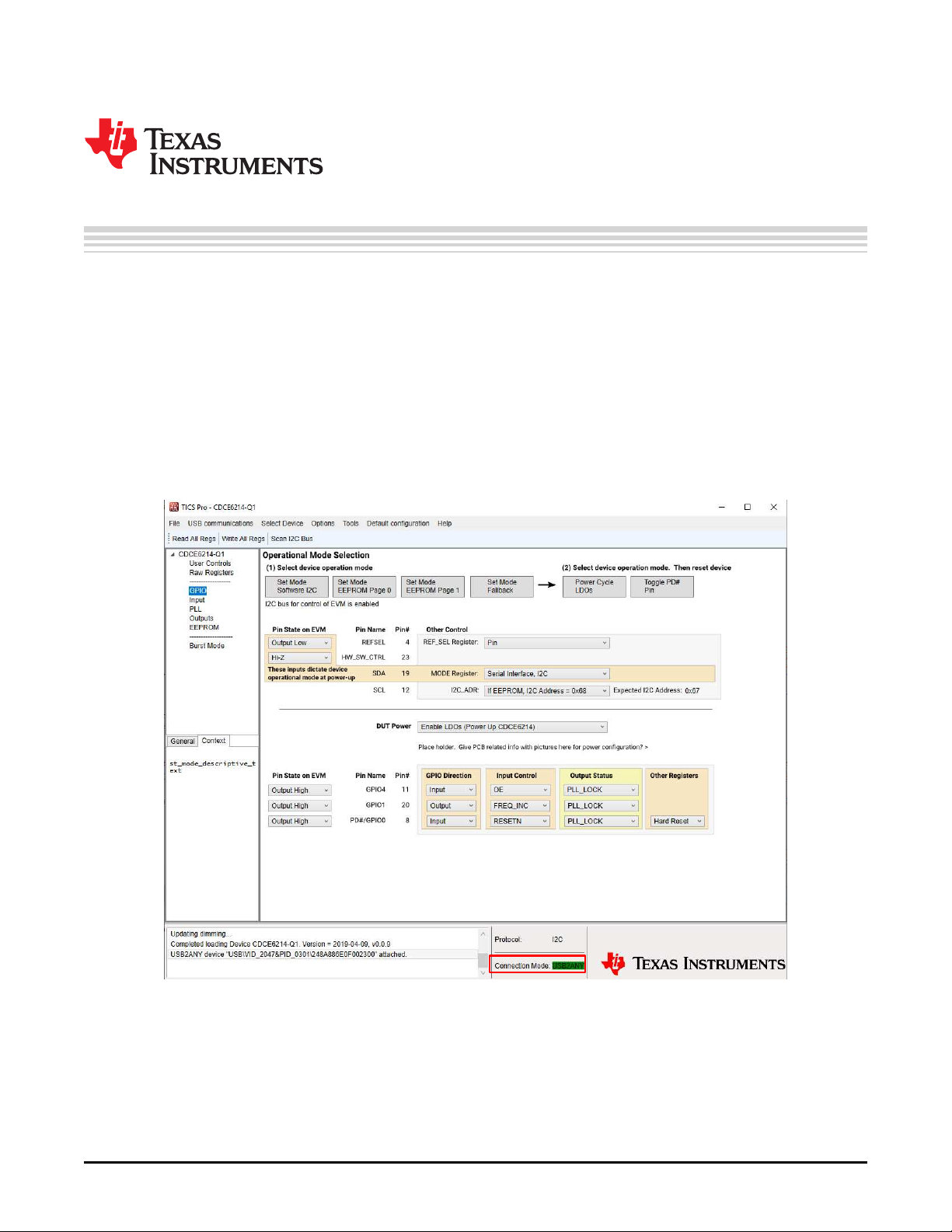
1.2 Connect the EVM to PC
Use a micro-B USB cable to connect the CDCE6214-Q1 EVM to the PC. Watch the "Connection mode"
field turn green on the screen. If the connection mode stays red, follow the instructions listed in
Section 3.1
Chapter 1
SNAU244–July 2019
Quick Start
Figure 1-1. TICS Pro Snapshot With USB2ANY Connected
4
Quick Start
Copyright © 2019, Texas Instruments Incorporated
Submit Documentation Feedback
SNAU244–July 2019
Page 5
1
2
34
www.ti.com
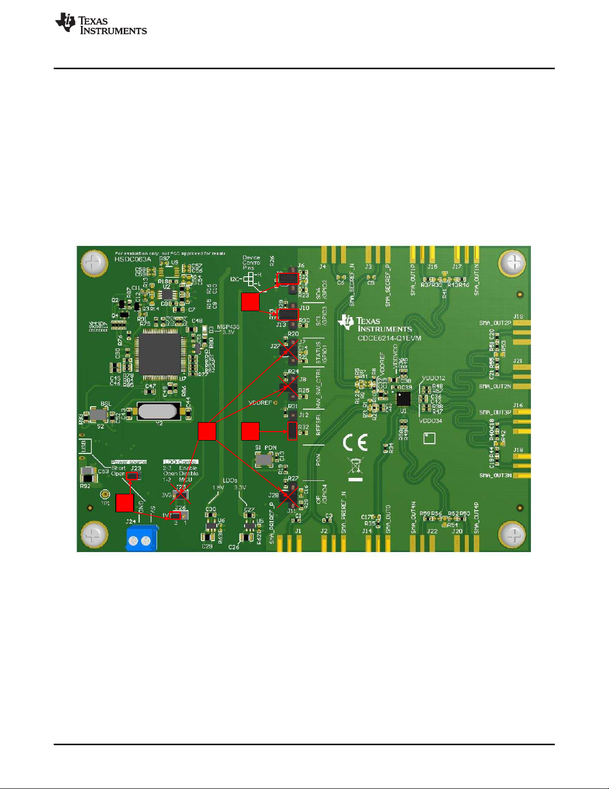
1.3 Configure Jumpers
To configure the jumpers:
1. Unplug the USB from the EVM to disconnect the power.
2. Short J23 to power the on-board LDOs with a 5-V source from the USB. Short pins 2 and 3 of J26 to
enable 1.8-V LDOs.
3. Short pin 2 of J6 and pin 1 of J9. Short pin 2 of J10 and pin 1 of J13. The purpose of this step is to
connect SCL and SDA pins of DUT to the on-board microcontroller in order to enable I2C
programming.
4. Short pin 1 and 2 of J12 to pull the REFSEL pin low. When the REFSEL pin is low, select the
secondary reference and use an on-board 25-MHz crystal as the reference source.
5. Remove all other jumpers or leave them floating by connecting them to only one pin. The position of
J25 is not important because the resistors required to enable a 3.3-V rail are not populated by default.
Configure Jumpers
SNAU244–July 2019
Submit Documentation Feedback
Figure 1-2. Jumper Configuration Guideline
Copyright © 2019, Texas Instruments Incorporated
Quick Start
5
Page 6
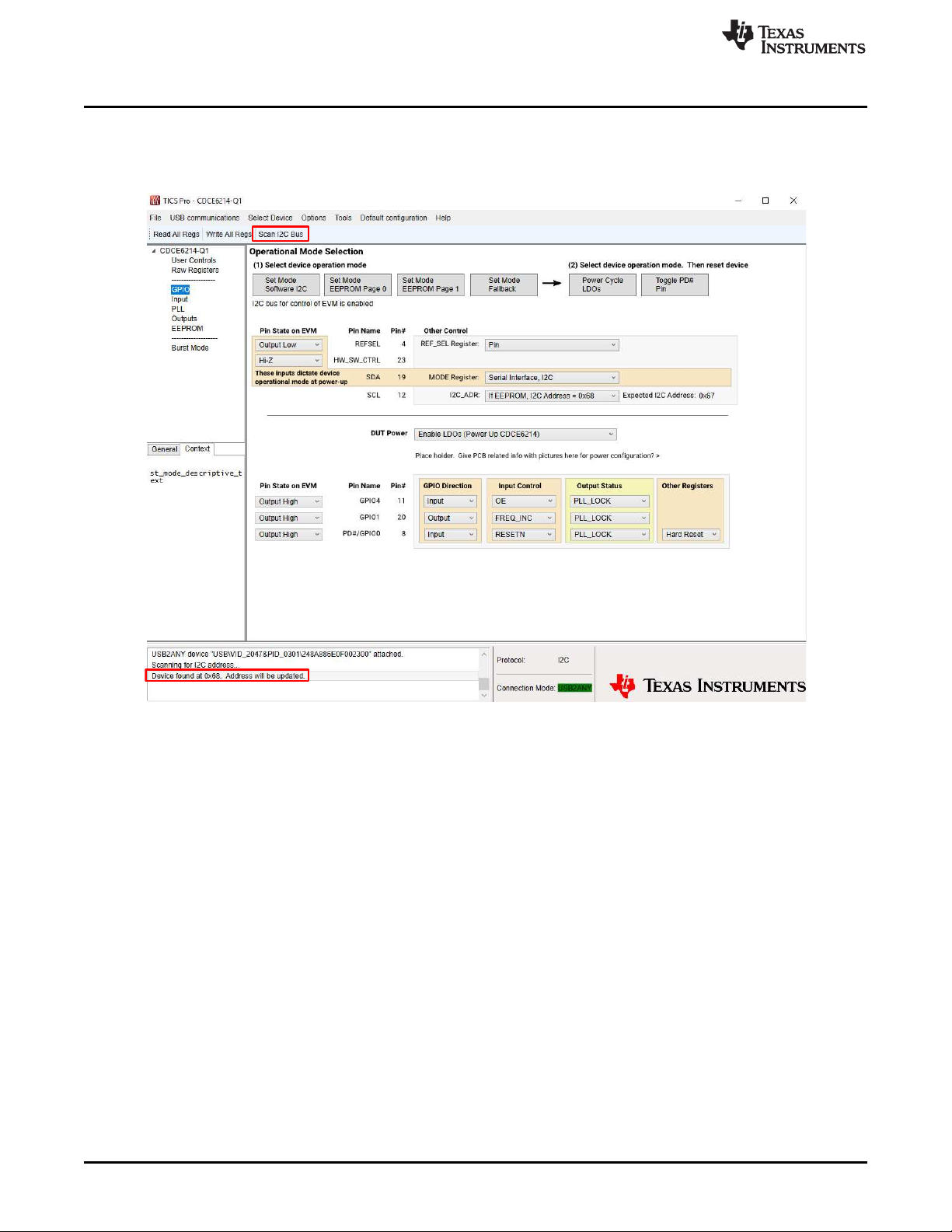
Scan I2C Bus
1.4 Scan I2C Bus
Click the "Scan I2C Bus" in the small toolbar. Look for the "Device found at 0x68. Address will be
updated." text in the message window.
www.ti.com
Figure 1-3. Scan I2C Bus
6
Quick Start
Copyright © 2019, Texas Instruments Incorporated
Submit Documentation Feedback
SNAU244–July 2019
Page 7
www.ti.com
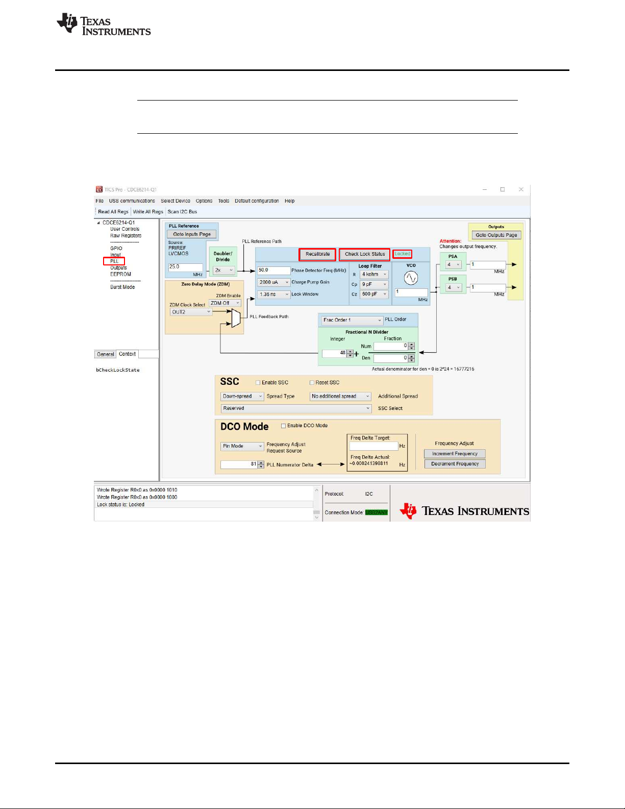
1.5 Load Default and Check Lock Status
NOTE: Hover over a register to read the register description in the bottom-left pane of the TICS Pro
window.
In the toolbar, go to "Default configurations" → "Default Startup". From there, go to "PLL" tab and select
the "Recalibrate" button, then "Check Lock Status". Watch for the green "locked" text to confirm that the
PLL is locked.
Load Default and Check Lock Status
SNAU244–July 2019
Submit Documentation Feedback
Figure 1-4. Check Lock Status
Copyright © 2019, Texas Instruments Incorporated
Quick Start
7
Page 8
Check Outputs
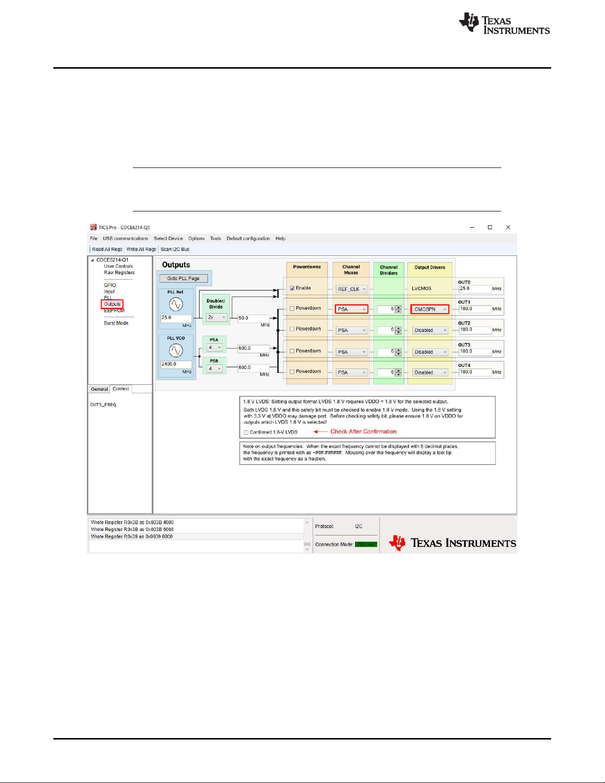
1.6 Check Outputs
The output frequency is saved as 1 MHz by default. To change the output frequency, go to the "Output"
page and update the text in Channel Muxes or Output Drivers columns shown in Figure 1-5. Change the
format of output 1 to "CMOSPN" to select the CMOS format output for both OUT1_P and OUT1_N, then
connect the SMA_OUT1P (J15) or SMA_OUT1N (J17) to an oscilloscope. With 50-Ω DC termination, see
the 100 MHz and close to 900 mV—half of the supply voltage with cable/connector loss—swing on the
scope.
NOTE: Only the SDA/GPIO2 and SCL/GPIO3 pins are connected to the on-board microcontroller.
The other pins can only be configured by the on-board jumpers or connected to an external
controller. They cannot be controlled by TICS Pro.
www.ti.com
Figure 1-5. Configure Outputs
8
Quick Start
Copyright © 2019, Texas Instruments Incorporated
Submit Documentation Feedback
SNAU244–July 2019
Page 9

2.1 Input Configuration
2.1.1 Input Selection
Two inputs—the "PRIREF" (primary reference) and "SECREF" (secondary reference)—are selected by a
combination of the register "REF_SEL" (R2[1:0]) and pin 4 "REFSEL". Register R2[1:0] overrides pin 4.
To enable pin control for input selection, go to TICS Pro "Input" page and set register "REF_SEL" to "Pin".
Pull pin "REFSEL" low (SECREF) or high (PRIREF) using jumper J12.
To use register control for input selection, set the register "REF_SEL" directly, For the primary reference,
feed reference source from SMA connectors J1 and/or J2. For the secondary reference, if crystal input is
preferred, refer to Section 2.1.2. Otherwise, populate C5. R7, C6, R11, J3, J4 and feed reference source
from SMA connectors J3 and/or J4.
Chapter 2
SNAU244–July 2019
Modes of Operations
SNAU244–July 2019
Submit Documentation Feedback
Copyright © 2019, Texas Instruments Incorporated
Modes of Operations
9
Page 10

Program biasing current
and load capacitance for
cystal
Register R2[1:0] for
input selection.
Input Configuration
2.1.2 Crystal Input
By default, register "ref_sel" is set to 0 and pin "REFSEL" is pulled low to enable the use of on-board 25MHz crystal. The designer can change the input bias current and load capacitance by programming the
registers highlighted in Figure 2-1. Note that the capacitance listed in the software is a single-ended value
at the drain and source. For example, if the load capacitance selected is 9.8 pF, the capacitance is 9.8 pF
at both the source and drain. Crystal vendors typically refer to load capacitance as effective series
capacitance seen by the crystal. So when 9.8 pF is selected, the real load capacitance should be 4.9 pF.
R5 and R12 are placeholders for external capacitors.
www.ti.com
2.2 PLL Configuration
On the TICS Pro "PLL" page, the designer can change input doubler/divider, loop filter component values,
charge pump gain, VCO frequency, fractional N divider, as well as prescaler A and B (PSA and PSB)
separately.
2.3 SSC, DCO and ZDM Modes
To configure SSC, DCO and ZDM modes, refer to the descriptions in the data sheet.
2.4 Output Configuration
10
On the TICS Pro "Outputs" page, the designer can program output channel MUX, integer output divider
values, as well as output format.
Modes of Operations
Figure 2-1. Input Configuration
Copyright © 2019, Texas Instruments Incorporated
Submit Documentation Feedback
SNAU244–July 2019
Page 11

www.ti.com
2.5 1.8-V and 3.3-V Power Supply
The 3.3-V LDOs are disabled by default, and the 1.8-V LDOs are controlled by J26. To enable the 1.8-V
LDOs, short pin 2 and 3 of J26. To disable the 1.8-V LDOs, remove the jumper for J26. To use 3.3-V
LDO, the designer must first populate the four 0-Ω resistors: R64, R66, R68, and R70. After the resistors
are populated, the 3.3-V LDOs are controlled by jumper J25. To enable the 3.3-V LDOs, short pin 2 and 3
of J25. To disable the 3.3-V LDOs, remove the jumper for J25.
Do NOT enable 1.8-V and 3.3-V LDOs at the same time.
1.8-V and 3.3-V Power Supply
WARNING
SNAU244–July 2019
Submit Documentation Feedback
Figure 2-2. Board Rework Guide to Enable 3.3-V Supply
Copyright © 2019, Texas Instruments Incorporated
Modes of Operations
11
Page 12

Frequently Asked Questions - FAQ
3.1 USB2ANY Cannot Be Detected By TICS Pro
3.1.1 Identify USB2ANY
In the TICS Pro, go to "USB communications" → "Interface" and make sure that the "USB2ANY" is
selected in the "Interface" group. Click "Identify" to see the blinking LED on the board. If this does not
work, try the next step.
Chapter 3
SNAU244–July 2019
Figure 3-1. USB2ANY Connection
3.1.2 Upgrade USB2ANY Firmware
If you are having issues with the USB2ANY, you can reload the firmware using the USB2ANY firmware
loader application. You can download it at http://www.ti.com/tool/USB2ANY (Explorer Software). When the
firmware is installed, navigate to the directory and select the USB2ANY firmware loader. Remember that
the S2 is the reset button in case you ever encounter a "hold down reset button while plugging the USB
cable" message. Note that the firmware loader only works on Windows 7 or lower versions of Windows
system. The firmware does not work on the Windows 10 system at the time of this user manual
publication.
12
Frequently Asked Questions - FAQ
Copyright © 2019, Texas Instruments Incorporated
Submit Documentation Feedback
SNAU244–July 2019
Page 13

SDA
SCL
5VGND
www.ti.com
3.2 How to Use External Microcontroller
The designer can use an external USB2ANY (http://www.ti.com/tool/USB2ANY) and blue wire the EVM.
However, the designer can only use a 3.3-V power supply because the USB2ANY only supports a 3.3-V
I2C bus.
3.2.1 Use 3.3-V Power Supply and Configure Jumpers
First follow the instructions on Section 2.5 to rework the board to enable 3.3-V LDOs. Follow these steps
and refer to Figure 3-2 to configure the jumpers
• Short J23. Short pins 2 and 3 of J25 and remove jumper for J26 to enable 3.3-V LDOs and disable
1.8-V LDOs.
• Short pins 2 and 3 of J6 and pins 2 and 3 of J10. The purpose is to disconnect the SDA and SCL pins
of DUT from on-board micocontroller and pull the SDA/SCL to VDDREF (3.3 V) through a 4.7-kΩ
resistor.
• Short pins 1 and 2 of J12 to use SECREF and on-board crystal.
• Remove all other jumpers (J7, J8, and J11).
• Connect GND, 5 V to ground, and the 5-V supply separately. Connect SDA (pin 2 of J6), SCL (pin 2 of
J10), and GND to USB2ANY. Refer to Figure 3-2 for details on how to connect these three wires to
USB2ANY.
How to Use External Microcontroller
SNAU244–July 2019
Submit Documentation Feedback
Figure 3-2. EVM Blue Wire Guide
Copyright © 2019, Texas Instruments Incorporated
Frequently Asked Questions - FAQ
13
Page 14

How to Use External Microcontroller
3.2.2 Connect SDA, SCL, and GND to USB2ANY
Refer to Figure 3-3 and connect the SDA, SCL and GND to pin 1, pin 2, and pin 5 of USB2ANY (J4 in
Figure 3-3) separately. The rectangle on the top indicates the slot of USB2ANY box.
www.ti.com
14
Frequently Asked Questions - FAQ
Figure 3-3. USB2ANY Pin Connection
Copyright © 2019, Texas Instruments Incorporated
Submit Documentation Feedback
SNAU244–July 2019
Page 15

4.1 Schematic
Chapter 4
SNAU244–July 2019
Schematic and Layout
SNAU244–July 2019
Submit Documentation Feedback
Figure 4-1. Schematic Page 1: Cover Sheet
Copyright © 2019, Texas Instruments Incorporated
Schematic and Layout
15
Page 16

Schematic
www.ti.com
16
Schematic and Layout
Figure 4-2. Schematic Page 2: USB
SNAU244–July 2019
Submit Documentation Feedback
Copyright © 2019, Texas Instruments Incorporated
Page 17

www.ti.com
Schematic
SNAU244–July 2019
Submit Documentation Feedback
Figure 4-3. Schematic Page 3: Power
Copyright © 2019, Texas Instruments Incorporated
Schematic and Layout
17
Page 18

Schematic
www.ti.com
18
Schematic and Layout
Figure 4-4. Schematic Page 4: Power Filter Distribution
SNAU244–July 2019
Submit Documentation Feedback
Copyright © 2019, Texas Instruments Incorporated
Page 19

www.ti.com
Schematic
SNAU244–July 2019
Submit Documentation Feedback
Figure 4-5. Schematic Page 5: Level Shifter
Copyright © 2019, Texas Instruments Incorporated
Schematic and Layout
19
Page 20

Schematic
www.ti.com
20
Schematic and Layout
Figure 4-6. Schematic Page 6: Input and Clock Generator
SNAU244–July 2019
Submit Documentation Feedback
Copyright © 2019, Texas Instruments Incorporated
Page 21

www.ti.com
Schematic
SNAU244–July 2019
Submit Documentation Feedback
Figure 4-7. Schematic Page 7: Outputs
Copyright © 2019, Texas Instruments Incorporated
Schematic and Layout
21
Page 22

Schematic
www.ti.com
22
Schematic and Layout
Figure 4-8. Schematic Page 8: EVM Hardware
SNAU244–July 2019
Submit Documentation Feedback
Copyright © 2019, Texas Instruments Incorporated
Page 23

www.ti.com
4.2 Layout
Layout
Figure 4-9. PCB Layer 1: Top Layer Composite
SNAU244–July 2019
Submit Documentation Feedback
Copyright © 2019, Texas Instruments Incorporated
Schematic and Layout
23
Page 24

Layout
www.ti.com
Figure 4-10. PCB Layer 2: Middle Layer
24
Schematic and Layout
Copyright © 2019, Texas Instruments Incorporated
Submit Documentation Feedback
SNAU244–July 2019
Page 25

www.ti.com
Layout
Figure 4-11. PCB Layer 3: Middle Layer
SNAU244–July 2019
Submit Documentation Feedback
Copyright © 2019, Texas Instruments Incorporated
Schematic and Layout
25
Page 26

Layout
www.ti.com
Figure 4-12. PCB Layer 4: Bottom Layer Composite
26
Schematic and Layout
Copyright © 2019, Texas Instruments Incorporated
Submit Documentation Feedback
SNAU244–July 2019
Page 27

IMPORTANT NOTICE AND DISCLAIMER
TI PROVIDES TECHNICAL AND RELIABILITY DATA (INCLUDING DATASHEETS), DESIGN RESOURCES (INCLUDING REFERENCE
DESIGNS), APPLICATION OR OTHER DESIGN ADVICE, WEB TOOLS, SAFETY INFORMATION, AND OTHER RESOURCES “AS IS”
AND WITH ALL FAULTS, AND DISCLAIMS ALL WARRANTIES, EXPRESS AND IMPLIED, INCLUDING WITHOUT LIMITATION ANY
IMPLIED WARRANTIES OF MERCHANTABILITY, FITNESS FOR A PARTICULAR PURPOSE OR NON-INFRINGEMENT OF THIRD
PARTY INTELLECTUAL PROPERTY RIGHTS.
These resources are intended for skilled developers designing with TI products. You are solely responsible for (1) selecting the appropriate
TI products for your application, (2) designing, validating and testing your application, and (3) ensuring your application meets applicable
standards, and any other safety, security, or other requirements. These resources are subject to change without notice. TI grants you
permission to use these resources only for development of an application that uses the TI products described in the resource. Other
reproduction and display of these resources is prohibited. No license is granted to any other TI intellectual property right or to any third
party intellectual property right. TI disclaims responsibility for, and you will fully indemnify TI and its representatives against, any claims,
damages, costs, losses, and liabilities arising out of your use of these resources.
TI’s products are provided subject to TI’s Terms of Sale (www.ti.com/legal/termsofsale.html) or other applicable terms available either on
ti.com or provided in conjunction with such TI products. TI’s provision of these resources does not expand or otherwise alter TI’s applicable
warranties or warranty disclaimers for TI products.
Mailing Address: Texas Instruments, Post Office Box 655303, Dallas, Texas 75265
Copyright © 2019, Texas Instruments Incorporated
 Loading...