

www.DataSheet4U.com
www.ti.com
EN
XIN
XOUT
VSS
VDD
FOUT
SDATA
1
2
3
4
5
6
8
» ´1mm 1mm
M0018-03
OSCILLATOR IC WITH ELECTRONIC CALIBRATION
CDCE401
SCAS820 – JUNE 2006
FEATURES
• Oscillator Gain Stage Implemented
• One LVCMOS Frequency Output
• Frequency Range of Oscillator Gain Stage =
20 MHz–100 MHz
• Frequency Range of LVCMOS Output = 0.625
MHz–100 MHz
• Electronic Trimming of Oscillator Using
Capacitance Arrays
• Programmable Post Dividers x, x/2, x/4, x/8,
x/16, x/32
• Nonvolatile Storage of Settings Using
EEPROM Technology
• Easy One-Wire In-Circuit Programming Allows
Programming and Trimming of Oscillator After
Manufacturing
• EEPROM Programming Without the Need to
Apply High Voltage to the Device
• Available as Die
• Small Form Factor From Less Than 1 mm × 1
mm, Allowing the Smallest Form Factor
Available for Today’s and Next-Generation
Oscillators
• Industrial Temperature Range –40°C to 85°C
• Wide VDD Range: 2.25 V up to 3.3 V
• ESD Protection Exceeds JESD22
– >2000-V Human-Body Model (A114-B)
– >200-V Machine Model (A115_A)
– >500-V Charged-Device Model (C101-B.01)
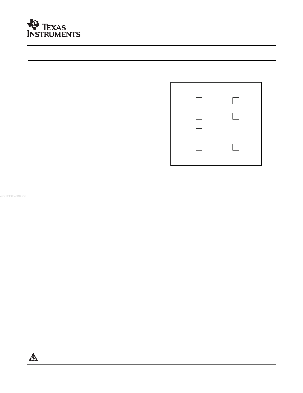
Die Terminal Assignment
(Top View = Bond Pad View)
DESCRIPTION
The CDCE401 is designed to achieve today’s demanding challenges for crystal oscillator modules. The small
form factor of the unpackaged die or the QFN package reduces the space consumption of the device to the
technical minimum level of today’s silicon technology.
The on-die trimming capacitance allows frequency trimming of the oscillator module after the manufacturing
process. Therefore, by doing a post-manufacturing programming, crystal manufacturing tolerances can be
trimmed out.
During power up or with each enabling, the CDCE401 oscillator start-up circuit switches off all oscillator
capacitors (CXI, CXO, CBASE) to maximize negative impedance during start-up. After a certain time
(1/XTAL-frequency × 2
frequency range.
Please be aware that an important notice concerning availability, standard warranty, and use in critical applications of Texas
Instruments semiconductor products and disclaimers thereto appears at the end of this data sheet.
PRODUCTION DATA information is current as of publication date.
Products conform to specifications per the terms of the Texas
Instruments standard warranty. Production processing does not
necessarily include testing of all parameters.
17
~ 1.311 ms–6.554 ms), the capacitances are connected to tune to the trimmed
Copyright © 2006, Texas Instruments Incorporated
www.ti.com
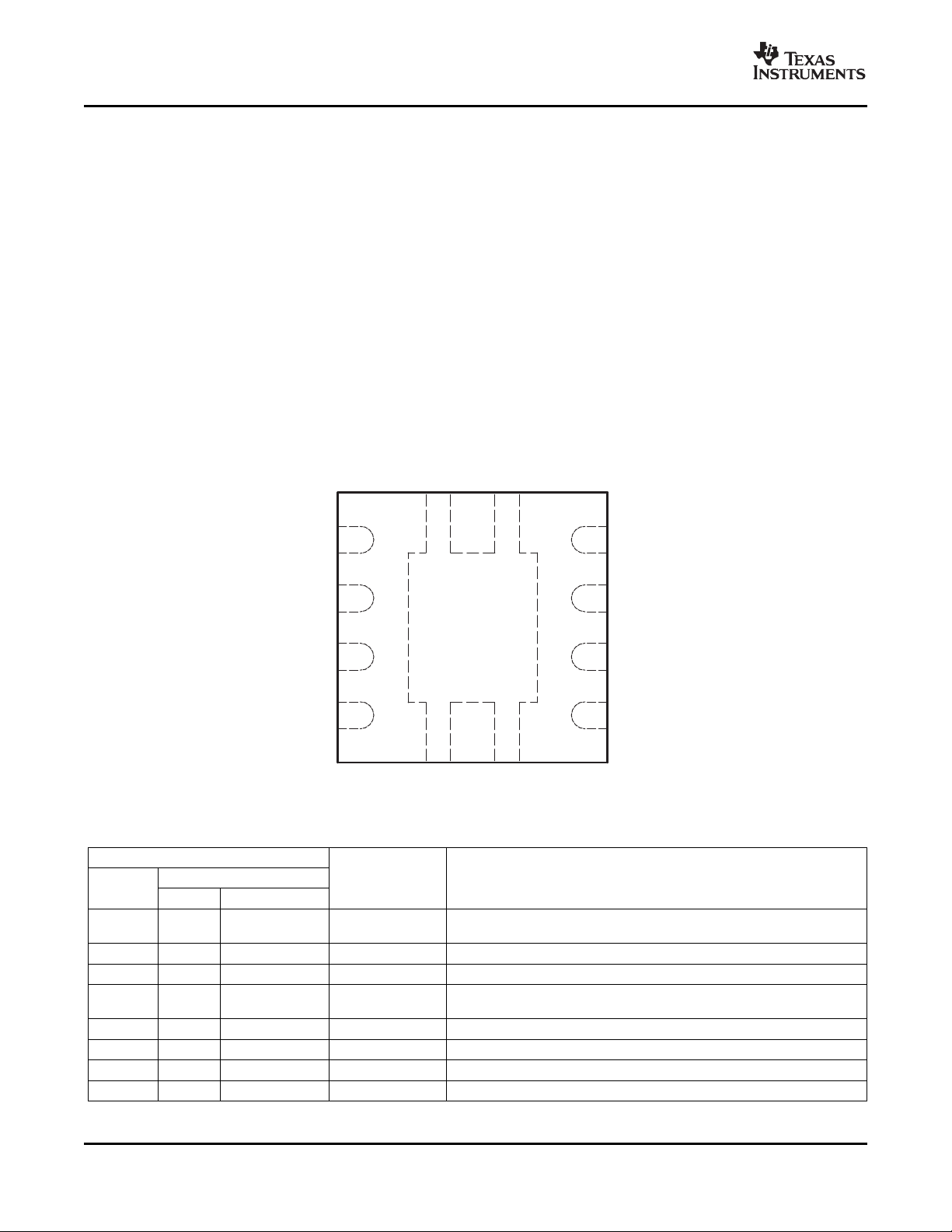
EN VDD1
DRB PACKAGE
(TOP VIEW)
NC − No internal connection
2
3
4
8
7
6
5
XIN NC
XOUT SDATA
VSS FOUT
P0012-01
CDCE401
SCAS820 – JUNE 2006
An on-die EEPROM enables nonvolatile storage of the frequency setting. For the transfer of the programming
into the EEPROM, the CDCE401 takes advantage of the SDATA input. In-circuit programming of the device is
possible.
Unlike other EEPROM-based devices, it is not necessary to apply a high supply voltage to the device in order to
program it.
The CDCE401 accepts crystals from 20 MHz up to 100 MHz. For lower frequencies, the CDCE401 provides a
programmable post-divider.
The CDCE401 features a wide supply-voltage range. This makes the device ideal to use at today’s most
commonly used supply voltage of 2.5 V, and operation at supply voltages of 2.8 V, 2.85 V, and 3 V for cellular
applications can be addressed with a single device. Therefore, use of the device in multiple different application
spaces is possible, reducing inventory costs.
The CDCE401 is characterized to work in the industrial temperature range from –40°C to 85°C.
Optional: QFN Package Terminal Assignment
For evaluation purposes, the CDCE401 is also available in a QFN package. The packaged device can be
obtained together with an EVM.
Table 1. TERMINAL FUNCTIONS
TERMINAL
NAME
EN 1 1 Input LVCMOS
FOUT 5 5 Output LVCMOS Frequency output
NC 7 N/A Not connected
SDATA 6 7 Input LVCMOS
VDD 8 8 Power Voltage supply
VSS 4 4 Ground Ground
XIN 2 2 Input oscillator Crystal oscillator input
XOUT 3 3 Output oscillator Crystal oscillator output
2
NUMBER TYPE DESCRIPTION
QFN BOND PAD
Logic select pin. Enables/disables device. Has a hysteresis of 300 mV. A
2-M Ω pullup resistor is built in.
Logic select pin. This input serves as programming input. Has a
hysteresis of 300 mV. A 2-M Ω pullup resistor is built in.
Submit Documentation Feedback
www.ti.com
XIN
OG[1:0]
OG[1:0]
OP[2:0]
OG[1:0]
PD[2:0]
EN
FOUT
XOUT
VSS
CXOUT
C
BASE
CXOUT
C
BASE
Var
C
BASE
Var
C
BASE
C
L
C
L
CXO[7:0]
Read-Back
Mode
CXI[7:0]
Oscillator
Gain
Stage
EEPROM
and
Control
Logic
SDATA
2MW
VDD
Divider
P
Bias
M
U
X
2MW
B0027-03
LVCMOS
LVCMOS
LVCMOS
FUNCTIONAL BLOCK DIAGRAM
CDCE401
SCAS820 – JUNE 2006
Submit Documentation Feedback
3
www.ti.com
T0130-01
VDD
EnterProgramming
SequenceandWrite
Word0(TrimPPM)
EN/SDATA
Apply Application
VDDandVerify
Settings(Measure)
Perform
StateJump
Into
Program
EEPROM
HoldforMinimum
10msto Achieve
SafeProgramming
JumpFrom
State3 State1®
BackIntoNormal
Application After
200- sLowm
2.25V VDD 3.3V£ £
3.1V VDD 3.3V£ £3.1V VDD 3.3V£ £
2.25V VDD 3.3V£ £
CDCE401
SCAS820 – JUNE 2006
DETAILED DESCRIPTION
CONTROL PIN EN: Enable
The functions of the EN control pin are listed and explained in Table 2 .
Table 2. EN Control Pin Functions
EN FUNCTION
0 Disabled: all current sources are switched off, output is in the high-impedance state.
1 Enabled: output follows the XIN/XOUT oscillation.
SINGLE-PIN INTERFACE CONTROL COMMANDS
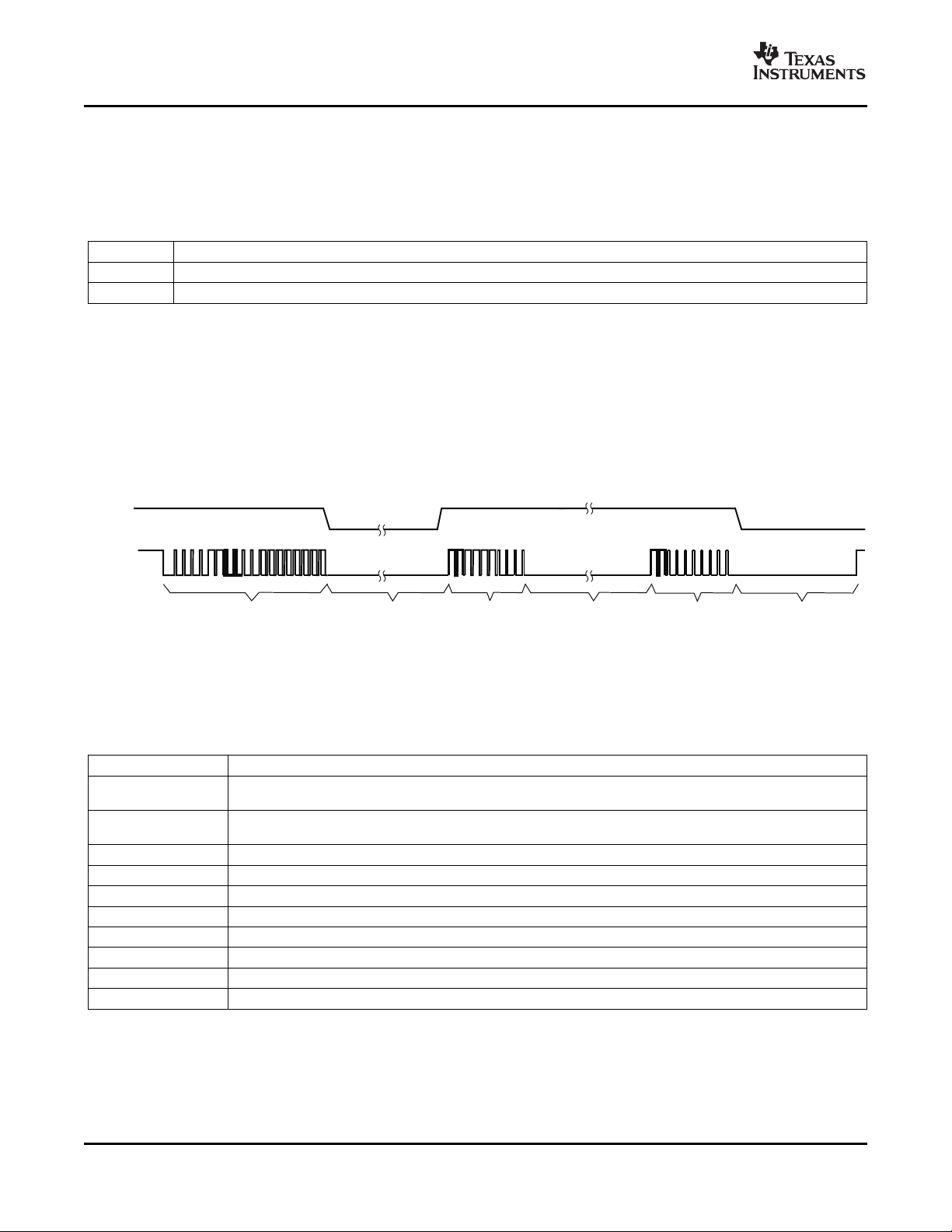
The CDCE401 can be configured and programmed via the SDATA input pin. For this purpose, a
pulse-code-shaped signal must be applied to the device as shown in the waveforms of Figure 1 to select one of
the operation modes described in the State Flow-Diagram of the Single-Pin Interface section. During the
EEPROM programming phase, the device requires a stable VDD of 3.2 V ±100 mV for secure writing of the
EEPROM cells. After each Write-to-WordX, the written data is latched, made effective, and offers look-ahead
before the actual data is stored into the EEPROM.
Table 3 summarizes all valid programming commands.
Figure 1. Typical Programming Cycle
Table 3. Single-Pin Interface Control Commands
SDATA FUNCTION
00 1100 Enter register programming mode (state 1 → state 2); bits must be sent in the specified order with the specified
11 1011 Enter register read-back mode; bits must be sent in the specified order with the specified timing. Otherwise a
00 xxxx xxxx Write-to-word0 (state 2)
10 xxxx xxxx Write-to-word1 (state 2)
01 xxxx xxxx Write-to-word2 (state 2)
11 xxxx xxxx State-machine jump: All other patterns not defined as follows cause exit to normal mode.
11 1111 1111 Jump: Exit write-to-RAM (state 2 → state 1)
11 1111 0000 Jump: Enter EEPROM programming without an EEPROM lock (state 2 → state 3)
11 0101 0101 Jump: Enter EEPROM programming with EEPROM lock (state 2 → state 4)
11 0000 0000 Jump: Exit EEPROM programming (state 3 or state 4 → state 1)
(1) Each rising edge causes a bit to be latched.
(2) Between the bits, some longer time delays can occur, but this has no effect on the data.
(3) A Write-to-WordX is expected to be 10 bits long. After the 10
look-ahead function.
timing. Otherwise, a time-out occurs.
time-out occurs.
(1) (2) (3)
(1) (2) (3)
(1) (2) (3)
th
bit, the respective word is latched, and its effect can be observed as
4
Submit Documentation Feedback
www.ti.com
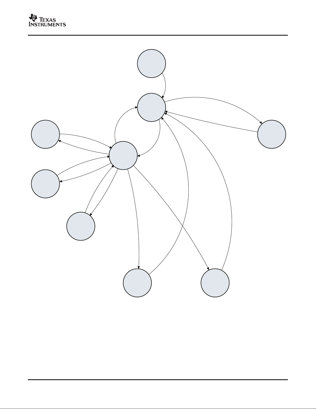
STATE FLOW-DIAGRAM OF THE SINGLE-PIN INTERFACE
F0016-01
PowerUp:
Read
EEPROM
and
Configure
State1: IDLE
Normal
Operation
State2:
Register
Programming
Mode
State3:
Program
EEPROM
NoLocking
State4:
Program
EEPROM
WithLocking
Write
Word2
Write
Word1
Write
Word0
State5:
Register
Read-Back
Mode
Power-UpReset
Completed
SDATA =
1111111111
SDATA =
0000000011
SDATA =
0101010111
SDATA =
1111000011
SDATA =
xxxxxxxx01
SDATA =
xxxxxxxx00
SDATA =
xxxxxxxx10
SDATA =
0000000011
SDATA =
001100
SDATA =
111011
30 Clock
Applied
th
10 Bit
Written
th
10 Bit
Written
th
10 Bit
Written
th
CDCE401
SCAS820 – JUNE 2006
NOTE: In states 2, 3, 4, and 5, the signal pin EN is disregarded and has no influence on power down.
Submit Documentation Feedback
5
www.ti.com
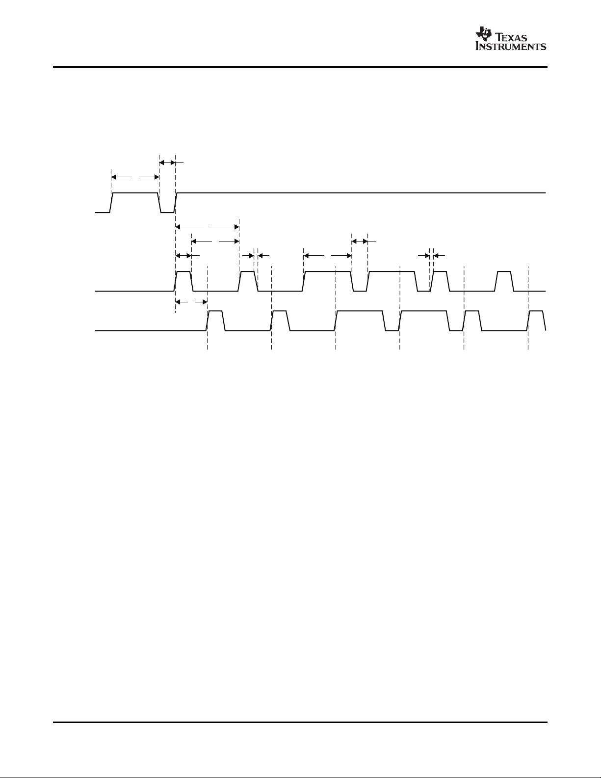
SDATA
EN
0
t
2
DATA
0 1 1 0 0
SDATA
DELAYED
t
1
t
6
t
f
t
5
t
4
t
8
t
r
T0042-03
t
3
t
7
CDCE401
SCAS820 – JUNE 2006
ENTER REGISTER PROGRAMMING MODE
Figure 2 shows the timing behavior of data to be written into SDATA. The sequence shown is 00 1100. If the
high period is as short as t1, this is interpreted as a 0. If the high period is as long as t3, this is interpreted as
a 1. This behavior is achieved by shifting the incoming signal SDATA by time t5into signal SDATA_DELAYED.
As can be seen in Figure 2 , SDATA_DELAYED can be used to latch (or strobe) SDATA. The specification for
the timings t1– t8, tr, and tfare given in the Timing Requirements section of this document.
Figure 2. Timing Diagram for SDATA Programming
6
Submit Documentation Feedback

www.ti.com
EnterProgramming Sequence
Word0
After8bits,thepayload
dataistransferredto
theRAMandisactive.
Waitforatleast
10msbefore
exitingEEPROM
writephase,for
safeoperation.
Payload
Word1
Payload
Word2
Payload
State
Machine
Jump
State
Machine
Jump
State2 ® State3
State3 ® State1
T0043-02
CDCE401
SCAS820 – JUNE 2006
TYPICAL CYCLE, PROGRAMMING THREE WORDS INTO EEPROM
Figure 3 shows an enter register programming mode and how the different words can be written. Bold highlights
the addressing of word0–word2. After that, the payload for the respective word is clocked in. In this example,
this is followed by a jump from state 2 → state 3 into enter EEPROM programming with EEPROM lock. In the
EEPROM-programming state, it is necessary to wait at least 10 ms for safe programming. The last command is
a jump from state 3 into state 1 (normal operation).
TYPICAL WRITE/VERIFY/PROGRAM CYCLE
As stated previously in this document, for safe writing and programming, the supply voltage must be held within
a narrow window of 3.2 V ±100 mV. Figure 1 illustrates writing to the device and verifying the settings, followed
by a safe programming into EEPROM.
Figure 3. EEPROM Programming Example
Submit Documentation Feedback
7

www.ti.com
T0044-02
0
0
1 1 1 1 1
1 2
26
27
28
SDATA
FOUT
EnterRegister
Read-BackMode
Fetch
EEPROM
ContentWith
1 CLK
st
EEPROMContent
1 Bit Available After
1 FallingEdge
st
st
30 FallingEdge
SwitchesBackInto
NormalOperation
th
OutputOscillation
OutputOscillation
CDCE401
SCAS820 – JUNE 2006
ENTER REGISTER READ-BACK MODE
Similar to the enter registerprogramming mode sequence, the enter register read-back mode is written into
SDATA. Before the enter register read-back mode is written, the device must be disabled via EN for 100 µ s to
ensure that the EEPROM content is read out correctly with enter register read-back mode. After the command
has been issued, the SDATA input is reconfigured as a clock input. By applying one clock, the EEPROM content
is read into shift registers. Now, by further applying clocks at SDATA, the EEPROM content can be clocked out
and observed at FOUT. Also, FOUT is reconfigured during that operation, as can be seen in the following figure.
There are 29 bits to be clocked out. With the 30
normal operation.
Figure 4. Typical Register Read-Back Cycle
th
falling clock edge, the FOUT pin is reconfigured back to
In Table 4 , the content of the bits in the output stream is summarized. Note that the MSB is clocked out first.
Table 4. Read-Back Cycle Bit Stream
OUTPUT-STREAM BITS FUNCTION
Bits[0:2] Revision identifier (MSB first)
Bit[3] EEPROM status:
Bit[4] EEPROM lock:
Bits[5:12] Storage value, word2 (MSB first)
Bits[13:20] Storage value, word1 (MSB first)
Bits[21:28] Storage value, word0 (MSB first)
0 = EEPROM has never been written.
1 = EEPROM has been programmed before.
0 = EEPROM can be rewritten.
1 = EEPROM is locked; rewriting to the EEPROM is not possible.
8
Submit Documentation Feedback
www.ti.com
REGISTER DESCRIPTION
WORD 0:
BIT NAME DESCRIPTION/FUNCTION TYPE DEFAULT
0 C0 Register selection W 0
1 C1 Register selection W 0
2 CXI0 Load capacitance XIN, bit 0 W 0
3 CXI1 Load capacitance XIN, bit 1 W 0
4 CXI2 Load capacitance XIN, bit 2 W 0
5 CXI3 Load capacitance XIN, bit 3 W 0
6 CXI4 Load capacitance XIN, bit 4 W 0
7 CXI5 Load capacitance XIN, bit 5 W 1
8 CXI6 Load capacitance XIN, bit 6 W 1
9 CXI7 Load capacitance XIN, bit 7 W 0
WORD 1:
BIT NAME DESCRIPTION/FUNCTION TYPE DEFAULT
0 C0 Register selection W 1
1 C1 Register selection W 0
2 CXO0 Load capacitance XOUT, bit 0 W 0
3 CXO1 Load capacitance XOUT, bit 1 W 0
4 CXO2 Load capacitance XOUT, bit 2 W 0
5 CXO3 Load capacitance XOUT, bit 3 W 0
6 CXO4 Load capacitance XOUT, bit 4 W 0
7 CXO5 Load capacitance XOUT, bit 5 W 1
8 CXO6 Load capacitance XOUT, bit 6 W 1
9 CXO7 Load capacitance XOUT, bit 7 W 0
CDCE401
SCAS820 – JUNE 2006
WORD 2:
BIT NAME DESCRIPTION/FUNCTION TYPE DEFAULT
0 C0 Register selection W 0
1 C1 Register selection W 1
2 PD0 Post-divider selection, bit 0 W 0
3 PD1 Post-divider selection, bit 1 W 0
4 PD2 Post-divider selection, bit 2 W 0
5 OG0 Oscillator gain definition, bit 0
6 OG1 Oscillator gain definition, bit 1
7 OP0 Oscillator operating-point adjustment, bit 0
8 OP1 Oscillator operating-point adjustment, bit 1
9 OP2 Oscillator operating-point adjustment, bit 2
(1) The oscillator gain bits have impact on the capacitance C
bits OP[2:0] are used to set the bias point of the oscillator core stage. In combination with setting the post-divider ratio PD[2:0] = 111,
(1)
(1)
(1)
(1)
(1)
. See the table for input capacitance values. The oscillator operating-point
BASE
W 1
W 1
W 0
W 0
W 0
the current consumption can be optimized to set oscillator core current consumption for lower frequencies and higher frequencies. This
ensures that the oscillator core is in operating optimally for phase noise and low XTAL-drive power. Setting core power too high impacts
XTAL-drive power, which affects the lifetime of the crystal.
Submit Documentation Feedback
9

www.ti.com
CDCE401
SCAS820 – JUNE 2006
POST-DIVIDER SETTINGS
PD2 PD1 PD0 POST-DIVIDER SETTINGS COMMENT
0 0 0 Post-divider × 1 Default
0 0 1 Post-divider × 1/2
0 1 0 Post-divider × 1/4
0 1 1 Post-divider × 1/8
1 0 0 Post-divider × 1/16
1 0 1 Post-divider × 1/32
1 1 0 Test mode: turns off CXI, CXO, and C
Post-divider × 1 (like in default).
1 1 1 No division: The post-divider setting PD[2:0] = 111 is used to turn off the amplifier after the
oscillator core. This offers the capability to disable effectively all blocks except the oscillator
core (current consumption of core only can be measured and adjusted)
(1) Setting core current consumption too high impacts the crystal drive power, which affects crystal performance and lifetime.
.
BASE
(1)
.
RECOMMENDATIONS FOR OSCILLATOR GAIN
OG[1:0] OP[2:0] OSCILLATOR OSCILLATOR OPERATING FREQUENCY COMMENT
11 000 Oscillator gain for 20 MHz ≤ frequency < 40 MHz Default
10 000 Oscillator gain for 40 MHz ≤ frequency < 60 MHz
01 000 Oscillator gain for 60 MHz ≤ frequency < 80 MHz
00 000 Oscillator gain for 80 MHz ≤ frequency ≤ 100 MHz
(2) The oscillator gain bits have an impact on the capacitance C
whole supply voltage range. Depending on the crystal series equivalent resistance, the OP[2:0] bits might require different settings.
Contact TI for assistance.
(2)
AND OPERATING POINT DEFINITIONS
. See the table for input capacitance values. This table is valid for the
BASE
10
Submit Documentation Feedback

www.ti.com
CDCE401
SCAS820 – JUNE 2006
ABSOLUTE MAXIMUM RATINGS
over operating free-air temperature range (unless otherwise noted)
VDD Supply voltage range –0.5 to 8 V
V
V
Input voltage range
I
Output voltage range
O
Input current (V
I
O
θ
JA
T
stg
Continuous output current ±50 mA
Package thermal impedance:
Storage temperature range –65 to 150 °C
(2)
(2)
< 0, VI> VDD) ±20 mA
I
(3)
QFN8 package TBD K/W
(1) Stresses beyond those listed under absolute maximum ratings may cause permanent damage to the device. These are stress ratings
only, and functional operation of the device at these or any other conditions beyond those indicated under recommended operating
conditions is not implied. Exposure to absolute-maximum-rated conditions for extended periods may affect device reliability.
(2) The input and output negative voltage ratings may be exceeded if the input and output clamp-current ratings are observed.
(3) The package thermal impedance is calculated in accordance with JESD 51 (no-airflow condition) and JEDEC2S2P (high-k board).
RECOMMENDED OPERATING CONDITIONS
over operating free-air temperature range (unless otherwise noted)
SUPPLY VOLTAGES, CURRENTS AND TEMPERATURE RANGE
Supply voltage: the four target supply-voltage ranges are:
VDD b) 2.8 V ±10% = 2.52 V–3.08 V 2.25 3 3.3 V
VDD Supply voltage during configuration of the device and EEPROM writing 3.1 3.2 3.3 V
I
DD
I
DD(DIS)
T
A
LVCMOS INPUT PARAMETER (SDATA, EN)
V
IH
V
IL
R
PULLUP
LVCMOS OUTPUT PARAMETER (FOUT)
V
OH
V
OL
V
OH_12mA
V
OL_12mA
I
/I
OZH
a) 2.5 V ±10% = 2.25 V–2.75 V
c) 2.85 V ±10%= =2.56 V–3.14 V
d) 3 V ±10% = 2.7 V–3.30 V
Supply current f
CLOCK-max
3.3 V, C
L-max
Disable current fIN= 0 MHz, V
Operating free-air temperature –40 85 °C
High-level input voltage VDD = 3.3 V VDD – 0.5 VDD + 0.3 V
Low-level input voltage VDD = 3.3 V V
Pullup resistor (EN and SDATA) 1.4 2 3.5 M Ω
High-level output voltage IOH= –6 mA VDD – 0.3 V
Low-level output voltage IOL= 6 mA V
High-level output voltage IOH= –12 mA VDD – 0.6 V
Low-level output voltage IOL= 12 mA V
Output current in high-impedance state V
OZL
OUT
= VDD and V
(1)
= 100 MHz, V
= 15 pF
DD-max
OUT
VALUE UNIT
–0.5 to VDD + 0.5 V
–0.5 to VDD + 0.5 V
MIN NOM MAX UNIT
= 20 mA
DD-max
– 0.3 V
SS
= V
SS
+ 0.5 V
SS
+ 0.3 V
SS
+ 0.6 V
SS
10 µ A
±10 µ A
TIMING REQUIREMENTS
over recommended ranges of supply voltage, load, and operating free-air temperature
PARAMETER MIN NOM MAX UNIT
XIN/XOUT REQUIREMENTS
f
CLK_IN
f
Range
C
BASE_XIN
Crystal frequency 20 100 MHz
Trimming range (range is dependent on connected crystal) ±20 ppm
OG0 = 1 OG1 = 1 33
Base input capacitance into XIN, measured
single-ended with all CXx turned off
OG0 = 1 OG1 = 0 30
OG0 = 0 OG1 = 1 27
OG0 = 0 OG1 = 0 25
Submit Documentation Feedback
pF
11

www.ti.com
CDCE401
SCAS820 – JUNE 2006
TIMING REQUIREMENTS (continued)
over recommended ranges of supply voltage, load, and operating free-air temperature
PARAMETER MIN NOM MAX UNIT
OG0 = 1 OG1 = 1 25
C
BASE_XOUT
measured single-ended with all CXx turned pF
off
Crystal tune capacitance, measured single-ended against
CXI[7:0] VSS (subtracted from C
Base input capacitance into XOUT,
CXO[7:0] CXI[0:7] = C
CXO[0:7] = C
– C
XIN
XOUT
FOUT OUTPUT PARAMETER
f
CLK_OUT
tr/t
f
f
max
C
Load
Crystal frequency 20 100 MHz
Rise and fall time 10% to 90% VDD and 2 3 ns
Highest output frequency C
Load capacitance 15 pF
odc Output duty cycle
SDATA/EN TIMING
f
SDATACLK
t
1
t
2
t
3
t
4
t
5
t
6
t
7
t
8
tr/t
f
Repeat frequency of programming 200 kHz
LOW signal: high-pulse duration 0.5 1 1.2 µ s
LOW signal: low-pulse duration while entering programming sequence 3.8 4 4.2
LOW signal: low-pulse duration while programming bits 3.8
HIGH signal: high-pulse duration 3.8 4 4.5 µ s
HIGH signal: low-pulse duration while entering programming sequence 0.5 1 1.2
HIGH signal: low-pulse duration while programming bits 0.5
Time delay between SDATA signal and SDATA_Delayed signal at VDD = 3.3 V 1.5 2.5 3.5 µ s
Time between bits during enter programming mode and enter read-back mode 10 30 µ s
beyond which a time-out must occur
EN high time before first SDATA can be clocked in 60 µ s
EN low time before first SDATA bit is clocked in 2 10 µ s
Rise and fall time from 20% to 80% of VDD 1 15 ns
), i.e.:
BASE
(OGx) or
BASE
– C
(OGx)
BASE
OG0 = 1 OG1 = 0 17
OG0 = 0 OG1 = 1 16
OG0 = 0 OG1 = 0 11
C
Load,max
Load,max
At VDD/2, 20 MHz ≤ freq ≤ 80 45% 50% 55%
MHz
At VDD/2, 80 MHz < freq ≤ 40% 50% 60%
100MHz
CXx7 6
CXx6 3
CXx5 1.5
CXx4 0.75
CXx3 375
CXx2 187
CXx1 94
CXx0 47
= 15 pF
= 15 pF 100 MHz
pF
fF
µ s
µ s
12
Submit Documentation Feedback

www.ti.com
DEVICE CHARACTERISTICS
over recommended ranges of supply voltage, load, and operating free-air temperature (unless otherwise noted)
PARAMETER
Phase noise specifications under following assumptions for 20-MHz and 40-MHz crystals:
f = 20 MHz (L
f = 40 MHz (L
phn
10
phn
100
phn
1k
phn
10k
phn
100k
phn
1M
= 22.79 mH, CS= 2.78 fF, CP= 0.77 pF) and post-divider × 1
S
= 6.231 mH, CS= 2.541 fF, CP= 0.628 pF) and post-divider × 1
S
Phase noise at 10 Hz –65 dBc/Hz
Phase noise at 100 Hz –95 dBc/Hz
Phase noise at 1 kHz –125 dBc/Hz
Phase noise at 10 kHz –140 dBc/Hz
Phase noise at 100 kHz –145 dBc/Hz
Phase noise at 1 MHz –145 dBc/Hz
Phase noise specifications under following assumptions for 60-MHz and 80-MHz crystals:
f = 60 MHz (L
f = 80 MHz (L
phn
10
phn
100
phn
1k
phn
10k
phn
100k
phn
1M
= 2.015 mH, CS= 3.493 fF, CP= 0.876 pF) and post-divider × 1
S
= 0.907 mH, CS= 4.376 fF, CP= 1.156 pF) and post-divider × 1
S
Phase noise at 10 Hz –65 dBc/Hz
Phase noise at 100 Hz –95 dBc/Hz
Phase noise at 1 kHz –125 dBc/Hz
Phase noise at 10 kHz –133 dBc/Hz
Phase noise at 100 kHz –140 dBc/Hz
Phase noise at 1 MHz –145 dBc/Hz
Phase noise specifications under following assumptions for 100-MHz crystals:
f = 100 MHz (L
phn
10
phn
100
phn
1k
phn
10k
phn
100k
phn
1M
= 0.515 mH, CS= 4.923 fF, CP= 1.468 pF) and post-divider × 1
S
Phase noise at 10 Hz –65 dBc/Hz
Phase noise at 100 Hz –90 dBc/Hz
Phase noise at 1 kHz –120 dBc/Hz
Phase noise at 10 kHz –130 dBc/Hz
Phase noise at 100 kHz –135 dBc/Hz
Phase noise at 1 MHz –145 dBc/Hz
(1)
TEST CONDITIONS MIN TYP MAX UNIT
CDCE401
SCAS820 – JUNE 2006
(1) All parameters are defined for the test load given in SubSec1 5.1 .
Submit Documentation Feedback
13

www.ti.com
VDD
R=1kW
FromOutputofDUT
Out
LVCMOS
Output
R=1kW C =15pF
LOAD
S0034-02
FromOutputofDUT
LVCMOS
Output
R=50 W
C =100nF
C
S0199-01
CDCE401
SCAS820 – JUNE 2006
TEST LOAD CONDITION
Figure 5. LVCMOS Output Test Load for All Specifications Except Phase Noise Values
Figure 6. LVCMOS Output Test Load for Phase Noise Values
14
Submit Documentation Feedback

www.ti.com
CRYSTAL OSCILLATOR LEVEL CONVERSION
XIN
OG[1:0]
OG[1:0]
OP[2:0]
OG[1:0]
PD[2:0]
EN
FOUT
XOUT
VSS
OscillatorCaseWith4Pins
CXOUT
C
BASE
CXOUT
C
BASE
Var
C
BASE
Var
C
BASE
C
L
C
L
CXO[7:0]
Read-Back
Mode
CXI[7:0]
Oscillator
Gain
Stage
EEPROM
and
Control
Logic
SDATA
ENand
SDATA
2MW
VDD
Divider
P
Bias
+
–
M
U
X
2MW
B0027-04
LVCMOS
LVCMOS
LVCMOS
C =
15pF
LOAD
C =100nF
Filter
VSUPPLY
2.25V – 3.3V
CDCE401
SCAS820 – JUNE 2006
APPLICATION INFORMATION
Phase noise specifications under following assumptions:
Crystal with f = 40 MHz (L
phn
10
phn
100
phn
1k
phn
10k
phn
100k
phn
1M
Phase noise at 10 Hz VDD = 2.5 V –70 dBc/Hz
Phase noise at 100 Hz VDD = 2.5 V –100 dBc/Hz
Phase noise at 1 kHz VDD = 2.5 V –130 dBc/Hz
Phase noise at 10 kHz VDD = 2.5 V –145 dBc/Hz
Phase noise at 100 kHz VDD = 2.5 V –150 dBc/Hz
Phase noise at 1 MHz VDD = 2.5 V –150 dBc/Hz
Figure 7. Crystal Oscillator Application at 40 MHz in a 4-Pin Oscillator Case
PARAMETER TEST CONDITIONS MIN TYP MAX UNIT
= 10.534 mH, CS= 2.208 pF, CP= 0.551 pF) and post-divider × 1
S
Submit Documentation Feedback
15

www.ti.com
206
90
Note: AllUnits mm
964 – (WidthofSawBlade)
EN
XIN
XOUT
VSS
VDD
FOUT
SDATA
178
231
231
77
77
482 – (Widthof
SawBlade)/2
435
– (Widthof
SawBlade)/2
90
M0018-04
870 – (WidthofSawBlade)
CDCE401
SCAS820 – JUNE 2006
Figure 8. Die Dimensions (Top View – Bond Pad Locations)
16
Submit Documentation Feedback

PACKAGE OPTION ADDENDUM
www.ti.com
16-Apr-2007
PACKAGING INFORMATION
Orderable Device Status
(1)
Package
Type
Package
Drawing
Pins Package
Qty
Eco Plan
CDCE401YS PREVIEW XCEPT YS 0 Green (RoHS &
no Sb/Br)
(1)
The marketing status values are defined as follows:
ACTIVE: Product device recommended for new designs.
LIFEBUY: TI has announced that the device will be discontinued, and a lifetime-buy period is in effect.
NRND: Not recommended for new designs. Device is in production to support existing customers, but TI does not recommend using this part in
a new design.
PREVIEW: Device has been announced but is not in production. Samples may or may not be available.
OBSOLETE: TI has discontinued the production of the device.
(2)
Eco Plan - The planned eco-friendly classification: Pb-Free (RoHS), Pb-Free (RoHS Exempt), or Green (RoHS & no Sb/Br) - please check
http://www.ti.com/productcontent for the latest availability information and additional product content details.
TBD: The Pb-Free/Green conversion plan has not been defined.
Pb-Free (RoHS): TI's terms "Lead-Free" or "Pb-Free" mean semiconductor products that are compatible with the current RoHS requirements
for all 6 substances, including the requirement that lead not exceed 0.1% by weight in homogeneous materials. Where designed to be soldered
at high temperatures, TI Pb-Free products are suitable for use in specified lead-free processes.
Pb-Free (RoHS Exempt): This component has a RoHS exemption for either 1) lead-based flip-chip solder bumps used between the die and
package, or 2) lead-based die adhesive used between the die and leadframe. The component is otherwise considered Pb-Free (RoHS
compatible) as defined above.
Green (RoHS & no Sb/Br): TI defines "Green" to mean Pb-Free (RoHS compatible), and free of Bromine (Br) and Antimony (Sb) based flame
retardants (Br or Sb do not exceed 0.1% by weight in homogeneous material)
(2)
Lead/Ball Finish MSL Peak Temp
Call TI N / A for Pkg Type
(3)
(3)
MSL, Peak Temp. -- The Moisture Sensitivity Level rating according to the JEDEC industry standard classifications, and peak solder
temperature.
Important Information and Disclaimer:The information provided on this page represents TI's knowledge and belief as of the date that it is
provided. TI bases its knowledge and belief on information provided by third parties, and makes no representation or warranty as to the
accuracy of such information. Efforts are underway to better integrate information from third parties. TI has taken and continues to take
reasonable steps to provide representative and accurate information but may not have conducted destructive testing or chemical analysis on
incoming materials and chemicals. TI and TI suppliers consider certain information to be proprietary, and thus CAS numbers and other limited
information may not be available for release.
In no event shall TI's liability arising out of such information exceed the total purchase price of the TI part(s) at issue in this document sold by TI
to Customer on an annual basis.
Addendum-Page 1


IMPORTANT NOTICE
Texas Instruments Incorporated and its subsidiaries (TI) reserve the right to make corrections, modifications, enhancements,
improvements, and other changes to its products and services at any time and to discontinue any product or service without notice.
Customers should obtain the latest relevant information before placing orders and should verify that such information is current and
complete. All products are sold subject to TI’s terms and conditions of sale supplied at the time of order acknowledgment.
TI warrants performance of its hardware products to the specifications applicable at the time of sale in accordance with TI’s
standard warranty. Testing and other quality control techniques are used to the extent TI deems necessary to support this
warranty. Except where mandated by government requirements, testing of all parameters of each product is not necessarily
performed.
TI assumes no liability for applications assistance or customer product design. Customers are responsible for their products and
applications using TI components. To minimize the risks associated with customer products and applications, customers should
provide adequate design and operating safeguards.
TI does not warrant or represent that any license, either express or implied, is granted under any TI patent right, copyright, mask
work right, or other TI intellectual property right relating to any combination, machine, or process in which TI products or services
are used. Information published by TI regarding third-party products or services does not constitute a license from TI to use such
products or services or a warranty or endorsement thereof. Use of such information may require a license from a third party under
the patents or other intellectual property of the third party, or a license from TI under the patents or other intellectual property of TI.
Reproduction of information in TI data books or data sheets is permissible only if reproduction is without alteration and is
accompanied by all associated warranties, conditions, limitations, and notices. Reproduction of this information with alteration is an
unfair and deceptive business practice. TI is not responsible or liable for such altered documentation.
Resale of TI products or services with statements different from or beyond the parameters stated by TI for that product or service
voids all express and any implied warranties for the associated TI product or service and is an unfair and deceptive business
practice. TI is not responsible or liable for any such statements.
TI products are not authorized for use in safety-critical applications (such as life support) where a failure of the TI product would
reasonably be expected to cause severe personal injury or death, unless officers of the parties have executed an agreement
specifically governing such use. Buyers represent that they have all necessary expertise in the safety and regulatory ramifications
of their applications, and acknowledge and agree that they are solely responsible for all legal, regulatory and safety-related
requirements concerning their products and any use of TI products in such safety-critical applications, notwithstanding any
applications-related information or support that may be provided by TI. Further, Buyers must fully indemnify TI and its
representatives against any damages arising out of the use of TI products in such safety-critical applications.
TI products are neither designed nor intended for use in military/aerospace applications or environments unless the TI products are
specifically designated by TI as military-grade or "enhanced plastic." Only products designated by TI as military-grade meet military
specifications. Buyers acknowledge and agree that any such use of TI products which TI has not designated as military-grade is
solely at the Buyer's risk, and that they are solely responsible for compliance with all legal and regulatory requirements in
connection with such use.
TI products are neither designed nor intended for use in automotive applications or environments unless the specific TI products
are designated by TI as compliant with ISO/TS 16949 requirements. Buyers acknowledge and agree that, if they use any
non-designated products in automotive applications, TI will not be responsible for any failure to meet such requirements.
Following are URLs where you can obtain information on other Texas Instruments products and application solutions:
Products Applications
Amplifiers amplifier.ti.com Audio www.ti.com/audio
Data Converters dataconverter.ti.com Automotive www.ti.com/automotive
DSP dsp.ti.com Broadband www.ti.com/broadband
Interface interface.ti.com Digital Control www.ti.com/digitalcontrol
Logic logic.ti.com Military www.ti.com/military
Power Mgmt power.ti.com Optical Networking www.ti.com/opticalnetwork
Microcontrollers microcontroller.ti.com Security www.ti.com/security
Low Power www.ti.com/lpw Telephony www.ti.com/telephony
Wireless
Video & Imaging www.ti.com/video
Wireless www.ti.com/wireless
Mailing Address: Texas Instruments, Post Office Box 655303, Dallas, Texas 75265
Copyright © 2007, Texas Instruments Incorporated
 Loading...