

查询CDC9843供应商
CDC9843
PC MOTHERBOARD CLOCK SYNTHESIZER/DRIVER
WITH 3-STATE OUTPUTS
SCAS559C – DECEMBER 1995 – REVISED OCTOBER 1996
D
Provides System Clock Solution for
Pentium/82430HX/82430VX and
PentiumPro 82440FX Chipsets
D
Four Host-Clock Outputs With
Programmable Frequency
(50 MHz, 60 MHz, and 66 MHz)
D
Six PCI Clock Outputs at Half-CPU
Frequency
D
One 48-MHz Universal Serial Bus (USB)
Clock Output
D
One 24-MHz Floppy Controller Output
D
Two 14.318-MHz Reference Clock Outputs
D
All Output Clock Frequencies Derived From
Single 14.31818-MHz Crystal Input
D
LVTTL-Compatible Inputs and Outputs
D
Internal Loop Filters for Phase-Lock Loops
Eliminate the Need for External
Components
D
Operates at 3.3-V V
D
Packaged in Plastic Small-Outline Package
CC
description
V
CC
X1
X2
GND
OE
HCLK0
HCLK1
V
CC
HCLK2
HCLK3
GND
SEL1
SEL0
V
CC
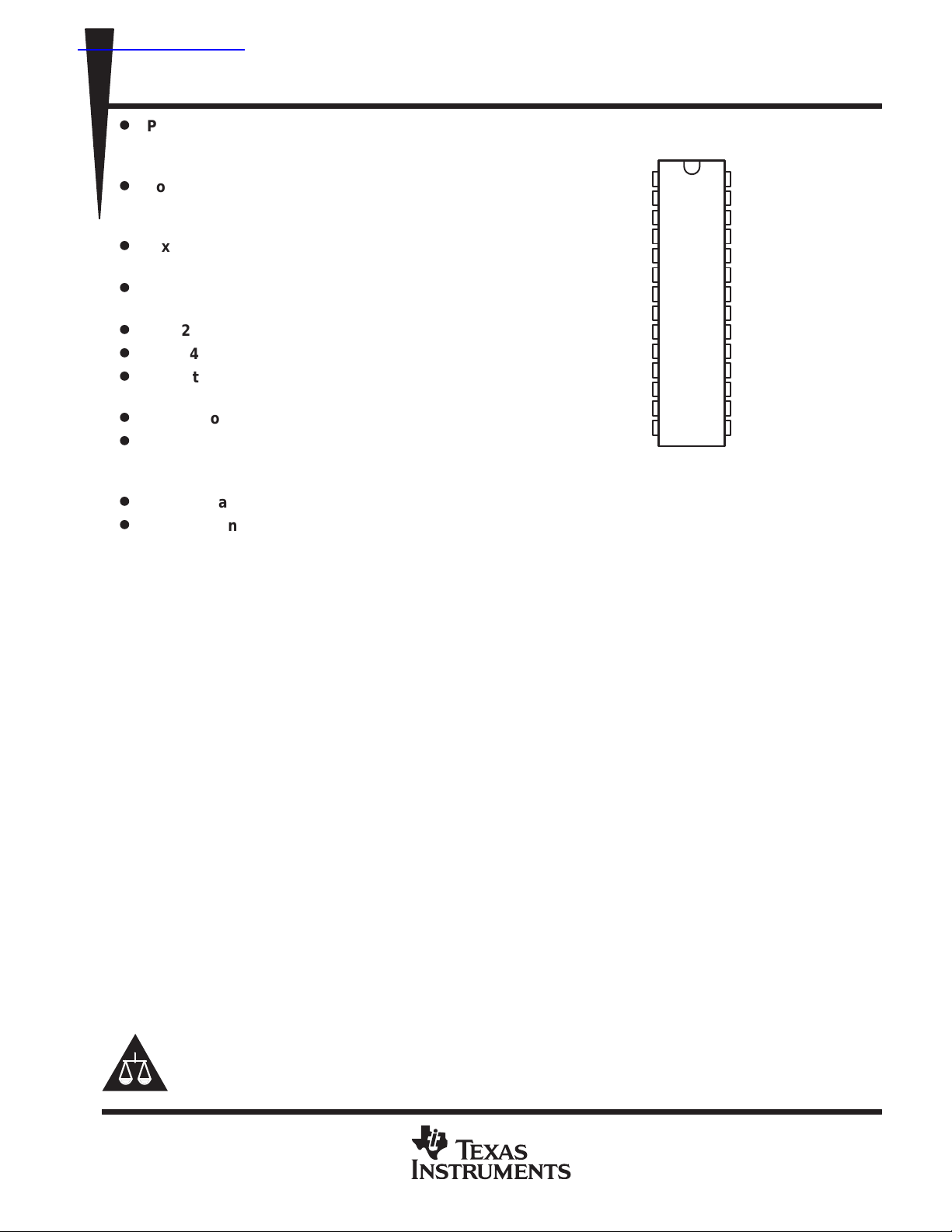
DW PACKAGE
(TOP VIEW)
1
28
2
27
3
26
4
25
5
24
6
23
7
22
8
21
9
20
10
19
11
18
12
17
13
16
14
15
REF0
REF1
V
CC
SBCLK
FCCLK
GND
PCLK0
PCLK1
V
CC
PCLK2
PCLK3
GND
PCLK4
PCLK5
The CDC9843 is a high-performance clock synthesizer/driver that generates the system clocks necessary to
support Pentium/82430HX/82430VX and PentiumPro 82440FX chipsets. Four host-clock outputs (HCLKn)
are programmable to one of three frequencies (50 MHz, 60 MHz, or 66 MHz) via the SEL0 and SEL1 control
inputs. Six PCI-clock outputs (PCLKn) are half the frequency of CPU clock outputs and are delayed 1 ns to
4 ns from the rising edge of the CPU clock. In addition, a universal serial bus (USB) clock output at 48 MHz
(SBCLK), a floppy controller clock at 24 MHz (FCCLK), and two 14.318-MHz reference clock outputs (REF0,
REF1) are provided.
All output frequencies are generated from a 14.318-MHZ crystal input. A reference clock input can be provided
at the X1 input instead of a crystal input.
Two phase-locked loops (PLLs) are used to generate the host clock frequency and the 48-MHz clock frequency .
On-chip loop filters and internal feedback eliminate the need for external components. The PCI-clock frequency
and floppy controller frequency are derived directly from the host-clock frequency and USB frequency,
respectively . The PLL circuit can be bypassed in the test mode (i.e., SEL0 = SEL1 = H) to distribute a test clock
provided at the X1 input.
The host- and PCI-clock outputs provide low-skew/low-jitter clock signals for reliable clock operation. All outputs
are 3 state and are enabled via OE.
Because the CDC9843 is based on PLL circuitry , it requires a stabilization time to achieve phase-lock of the PLL.
This stabilization time is required following power up and application of a fixed-frequency, fixed-phase signal
at the X1, as well as following any changes to the OE or SELn inputs.
Please be aware that an important notice concerning availability, standard warranty, and use in critical applications of
Texas Instruments semiconductor products and disclaimers thereto appears at the end of this data sheet.
Pentium is a trademark of Intel Corporation.
PRODUCTION DATA information is current as of publication date.
Products conform to specifications per the terms of Texas Instruments
standard warranty. Production processing does not necessarily include
testing of all parameters.
POST OFFICE BOX 655303 • DALLAS, TEXAS 75265
Copyright 1996, Texas Instruments Incorporated
1
CDC9843
PC MOTHERBOARD CLOCK SYNTHESIZER/DRIVER
WITH 3-STATE OUTPUTS
SCAS559C – DECEMBER 1995 – REVISED OCTOBER 1996
FUNCTION TABLE
OE
L X X 14.318 MHz Hi-Z Hi-Z Hi-Z Hi-Z Hi-Z
H L L 14.318 MHz 50 MHz 25 MHz 14.318 MHz 48 MHz 24 MHz
H L H 14.318 MHz 60 MHz 30 MHz 14.318 MHz 48 MHz 24 MHz
H H L 14.318 MHz 66 MHz 33 MHz 14.318 MHz 48 MHz 24 MHz
H H H TCLK
†
TCLK is a test-clock input at the X1 input during test mode.
SEL0 SEL1 X1 HCLKn PCLKn REFn SBCLK FCCLK
†
TCLK/2 TCLK/4 TCLK TCLK/4 TCLK/8
2
POST OFFICE BOX 655303 • DALLAS, TEXAS 75265
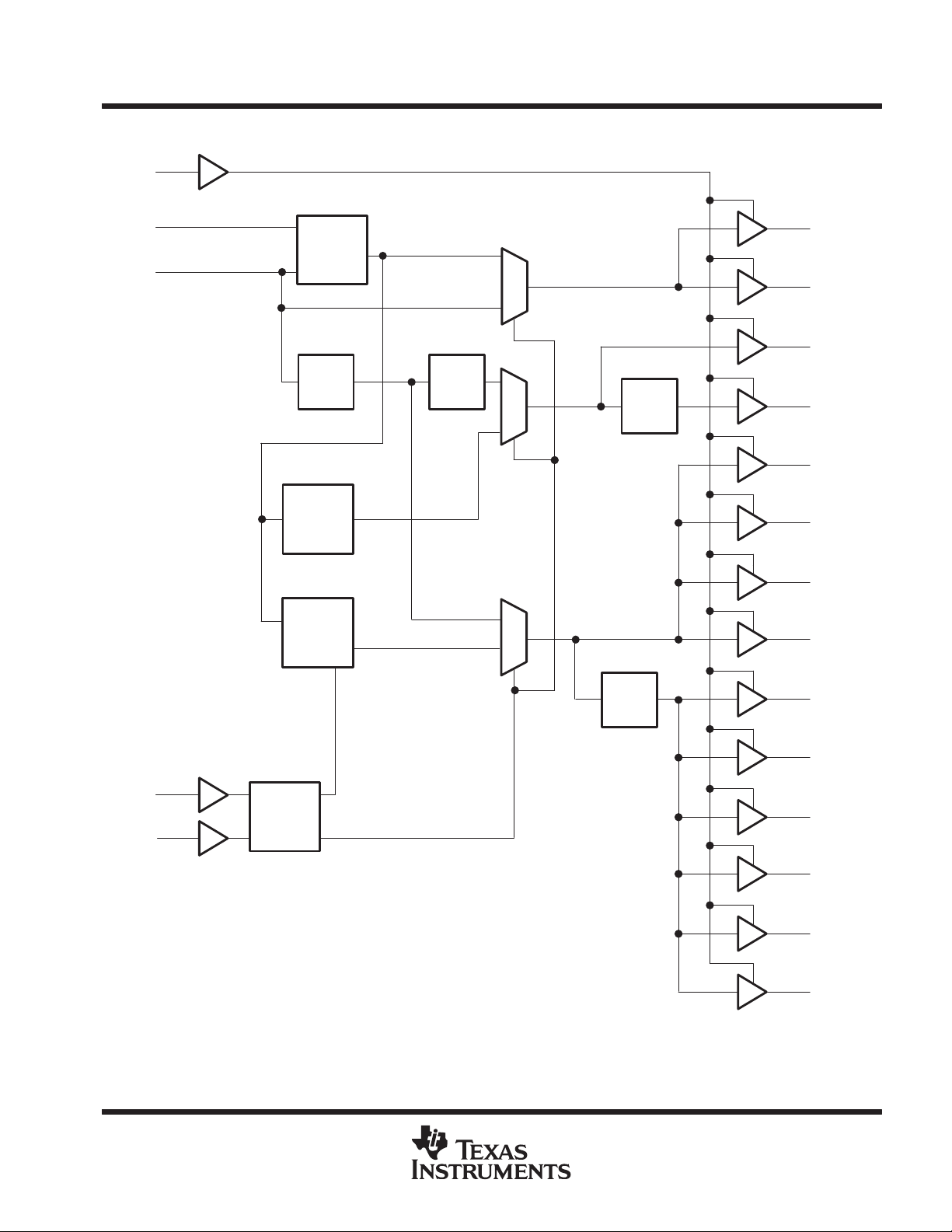
functional block diagram
5
OE
CDC9843
PC MOTHERBOARD CLOCK SYNTHESIZER/DRIVER
WITH 3-STATE OUTPUTS
SCAS559C – DECEMBER 1995 – REVISED OCTOBER 1996
X2
X1
3
OSC
2
÷2
48 MHz
PLL
CPU CLK
PLL
÷2
÷2
28
27
25
24
10
6
7
9
REF0
REF1
SBCLK
FCCLK
HCLK0
HCLK1
HCLK2
HCLK3
SEL0
SEL1
13
12
Select
Logic
÷2
16
18
19
21
22
15
PCLK5
PCLK4
PCLK3
PCLK2
PCLK1
PCLK0
POST OFFICE BOX 655303 • DALLAS, TEXAS 75265
3

CDC9843
I
CC
,
O
,
PC MOTHERBOARD CLOCK SYNTHESIZER/DRIVER
WITH 3-STATE OUTPUTS
SCAS559C – DECEMBER 1995 – REVISED OCTOBER 1996
absolute maximum ratings over operating free-air temperature range (unless otherwise noted)
Supply voltage range, V
Input voltage range, VI (see Note 1) –0.5 V to 4.6 V. . . . . . . . . . . . . . . . . . . . . . . . . . . . . . . . . . . . . . . . . . . . . . . . .
Voltage range applied to any output in the high-impedance state or power-off state,
VO (see Note 1) –0.5 V to VCC + 0.5 V. . . . . . . . . . . . . . . . . . . . . . . . . . . . . . . . . . . . . . . . . . . . . . . . . . . . . . . . . .
Current into any output in the low state, IO 16 mA. . . . . . . . . . . . . . . . . . . . . . . . . . . . . . . . . . . . . . . . . . . . . . . . . .
Input clamp current, I
Output clamp current, I
Maximum power dissipation at TA = 55°C (in still air) (see Note 2) TBD. . . . . . . . . . . . . . . . . . . . . . . . . . . . . . . .
Storage temperature range, T
†
Stresses beyond those listed under “absolute maximum ratings” may cause permanent damage to the device. These are stress ratings only, and
functional operation of the device at these or any other conditions beyond those indicated under “recommended operating conditions” is not
implied. Exposure to absolute-maximum-rated conditions for extended periods may affect device reliability.
NOTES: 1. The input and output negative-voltage ratings may be exceeded if the input and output clamp-current ratings are observed.
2. The maximum package power dissipation is calculated using a junction temperature of 150°C and a board trace length of 750 mils.
For more information, refer to the
Book
, literature number SCBD002.
–0.5 V to 4.6 V. . . . . . . . . . . . . . . . . . . . . . . . . . . . . . . . . . . . . . . . . . . . . . . . . . . . . . . . .
CC
(V
< 0) –18 mA. . . . . . . . . . . . . . . . . . . . . . . . . . . . . . . . . . . . . . . . . . . . . . . . . . . . . . . . . . .
IK
I
(V
OK
< 0) –50 mA. . . . . . . . . . . . . . . . . . . . . . . . . . . . . . . . . . . . . . . . . . . . . . . . . . . . . . . .
O
–65°C to 150°C. . . . . . . . . . . . . . . . . . . . . . . . . . . . . . . . . . . . . . . . . . . . . . . . . . .
stg
Package Thermal Considerations
application note in the
ABT Advanced BiCMOS T echnology Data
recommended operating conditions (see Note 3)
MIN MAX UNIT
V
CC
V
IH
V
IL
V
I
I
OH
I
OL
T
A
NOTE 3: Unused inputs must be held high or low to prevent them from floating.
Supply voltage 3.135 3.6 V
High-level input voltage 2 V
Low-level input voltage 0.8 V
Input voltage 0 V
High-level output current –8 mA
Low-level output current 8 mA
Operating free-air temperature 0 70 °C
CC
V
†
electrical characteristics over recommended operating free-air temperature range (unless
otherwise noted)
PARAMETER TEST CONDITIONS MIN TYP‡MAX UNIT
V
IK
V
OH
V
OL
I
I
I
OZ
CC
C
i
C
‡
All typical values are at VCC = 3.3 V.
§
Device in normal operating mode with no load on outputs
o
VCC = 3.135 V, II = –18 mA –1.2 V
VCC = 3.135 V, IOH = –8 mA 2.5 V
VCC = 3.135 V, IOL = 8 mA 0.4 V
VCC = 3.6 V, VI = VCC or GND ±1 µA
VCC = 3.6 V, VO = VCC or GND ±10 µA
V
= 3.6 V, I
VI = VCC or GND
VI = VCC or GND 6 pF
VI = VCC or GND 6 pF
= 0,
Outputs enabled
Outputs disabled 1 mA
§
50 mA
4
POST OFFICE BOX 655303 • DALLAS, TEXAS 75265

()
()
t
‡
Jitt
‡
‡
t
‡§
2
ns
t
‡§
2
ns
CDC9843
PC MOTHERBOARD CLOCK SYNTHESIZER/DRIVER
WITH 3-STATE OUTPUTS
SCAS559C – DECEMBER 1995 – REVISED OCTOBER 1996
timing requirements over recommended ranges of supply voltage and operating free-air
temperature
MIN MAX UNIT
After SEL1, SEL0 5
Stabilization time
†
Time required for the integrated PLL circuit to obtain phase lock of its feedback signal to its reference signal. In order for phase lock to be obtained,
a fixed-frequency, fixed-phase reference signal must be present at X1. Until phase lock is obtained, the specifications for propagation delay and
skew parameters given in the switching characteristics table are not applicable.
†
After OE↑ 5
After power up 5
switching characteristics (see Figures 1 and 2)
VCC = 3.135 V
PARAMETER
Skew
‡
Offset
er
Duty cycle
t
c
r
f
‡
Specifications are applicable only after the PLL stabilization time has elapsed.
§
Rise and fall times are characterized using the load circuits shown in Figure 1.
‡
FROM
(INPUT)
HCLKn PCLKn
HCKLn
PCLKn
TO
(OUTPUT)
HCLKn
PCLKn
HCKLn ±250 ps
PCKLn ±350 ps
Any output 45% 55%
SEL0 = L, SEL1 = L 20 ns
SEL0 = L, SEL1 = H 16.7 ns
SEL0 = H, SEL1 = L 15 ns
SEL0 = L, SEL1 = L 40 ns
SEL0 = L, SEL1 = H 33.3 ns
SEL0 = H, SEL1 = L 30 ns
HCLKn
PCKLn
HCKLn
PCLKn
to 3.6 V,
TA = 0°C to 70°C
MIN MAX
200 ps
400 ps
1 4 ns
ms
UNIT
POST OFFICE BOX 655303 • DALLAS, TEXAS 75265
5

CDC9843
PC MOTHERBOARD CLOCK SYNTHESIZER/DRIVER
WITH 3-STATE OUTPUTS
SCAS559C – DECEMBER 1995 – REVISED OCTOBER 1996
PARAMETER MEASUREMENT INFORMATION
CLOCK DRIVER CIRCUITS
From Output
Under Test
CL = 20 pF
(see Note A)
LOAD CIRCUIT
NOTES: A. CL includes probe and jig capacitance.
B. All input pulses are supplied by generators having the following characteristics: PRR v 10 MHz, ZO = 50 Ω, tr ≤ 2.5 ns,
tf ≤ 2.5 ns.
C. The outputs are measured one at a time with one transition per measurement.
500 Ω
Figure 1. Load Circuit and Voltage Waveforms
CPU Clock
(HCLK)
CPU Clock
(HCLK)
Skew
2.4 V
1.5 V
0.4 V
t
r
HCLK-to-HCLK Skew
t
c
Duty Cycle
t
f
VOLTAGE WAVEFORMS
V
OH
1.5 V
GND
1.5 V
V
OH
GND
PCI Clock
(PCLK)
CPU Clock
(HCLK)
PCI Clock
(PCLK)
Skew
PCLK-to-PCLK Skew
PCI Clock
(PCLK)
Offset
HCLK-to-PCLK Offset
Figure 2. Waveforms for Calculation of t
1.5 V
1.5 V
Offset
Skew
and t
1.5 V
1.5 V
V
GND
V
GND
offset
OH
OH
V
OH
GND
V
OH
GND
6
POST OFFICE BOX 655303 • DALLAS, TEXAS 75265

PACKAGE OPTION ADDENDUM
www.ti.com
30-Mar-2005
PACKAGING INFORMATION
Orderable Device Status
(1)
Package
Type
Package
Drawing
Pins Package
Qty
Eco Plan
CDC9843DW OBSOLETE SOIC DW 28 TBD Call TI Call TI
CDC9843DWR OBSOLETE SOIC DW 28 TBD Call TI Call TI
(1)
The marketing status values are defined as follows:
ACTIVE: Product device recommended for new designs.
LIFEBUY: TI has announced that the device will be discontinued, and a lifetime-buy period is in effect.
NRND: Not recommended for new designs. Device is in production to support existing customers, but TI does not recommend using this part in
a new design.
PREVIEW: Device has been announced but is not in production. Samples may or may not be available.
OBSOLETE: TI has discontinued the production of the device.
(2)
Eco Plan - The planned eco-friendly classification: Pb-Free (RoHS) or Green (RoHS & no Sb/Br) - please check
http://www.ti.com/productcontent for the latest availability information and additional product content details.
TBD: The Pb-Free/Green conversion plan has not been defined.
Pb-Free (RoHS): TI's terms "Lead-Free" or "Pb-Free" mean semiconductor products that are compatible with the current RoHS requirements
for all 6 substances, including the requirement that lead not exceed 0.1% by weight in homogeneous materials. Where designed to be soldered
at high temperatures, TI Pb-Free products are suitable for use in specified lead-free processes.
Green (RoHS & no Sb/Br): TI defines "Green" to mean Pb-Free (RoHS compatible), and free of Bromine (Br) and Antimony (Sb) based flame
retardants (Br or Sb do not exceed 0.1% by weight in homogeneous material)
(3)
MSL, Peak Temp. -- The Moisture Sensitivity Level rating according to the JEDEC industry standard classifications, and peak solder
temperature.
(2)
Lead/Ball Finish MSL Peak Temp
(3)
Important Information and Disclaimer:The information provided on this page represents TI's knowledge and belief as of the date that it is
provided. TI bases its knowledge and belief on information provided by third parties, and makes no representation or warranty as to the
accuracy of such information. Efforts are underway to better integrate information from third parties. TI has taken and continues to take
reasonable steps to provide representative and accurate information but may not have conducted destructive testing or chemical analysis on
incoming materials and chemicals. TI and TI suppliers consider certain information to be proprietary, and thus CAS numbers and other limited
information may not be available for release.
In no event shall TI's liability arising out of such information exceed the total purchase price of the TI part(s) at issue in this document sold by TI
to Customer on an annual basis.
Addendum-Page 1

IMPORTANT NOTICE
Texas Instruments Incorporated and its subsidiaries (TI) reserve the right to make corrections, modifications,
enhancements, improvements, and other changes to its products and services at any time and to discontinue
any product or service without notice. Customers should obtain the latest relevant information before placing
orders and should verify that such information is current and complete. All products are sold subject to TI’s terms
and conditions of sale supplied at the time of order acknowledgment.
TI warrants performance of its hardware products to the specifications applicable at the time of sale in
accordance with TI’s standard warranty. Testing and other quality control techniques are used to the extent TI
deems necessary to support this warranty . Except where mandated by government requirements, testing of all
parameters of each product is not necessarily performed.
TI assumes no liability for applications assistance or customer product design. Customers are responsible for
their products and applications using TI components. To minimize the risks associated with customer products
and applications, customers should provide adequate design and operating safeguards.
TI does not warrant or represent that any license, either express or implied, is granted under any TI patent right,
copyright, mask work right, or other TI intellectual property right relating to any combination, machine, or process
in which TI products or services are used. Information published by TI regarding third-party products or services
does not constitute a license from TI to use such products or services or a warranty or endorsement thereof.
Use of such information may require a license from a third party under the patents or other intellectual property
of the third party, or a license from TI under the patents or other intellectual property of TI.
Reproduction of information in TI data books or data sheets is permissible only if reproduction is without
alteration and is accompanied by all associated warranties, conditions, limitations, and notices. Reproduction
of this information with alteration is an unfair and deceptive business practice. TI is not responsible or liable for
such altered documentation.
Resale of TI products or services with statements different from or beyond the parameters stated by TI for that
product or service voids all express and any implied warranties for the associated TI product or service and
is an unfair and deceptive business practice. TI is not responsible or liable for any such statements.
Following are URLs where you can obtain information on other Texas Instruments products and application
solutions:
Products Applications
Amplifiers amplifier.ti.com Audio www.ti.com/audio
Data Converters dataconverter.ti.com Automotive www.ti.com/automotive
DSP dsp.ti.com Broadband www.ti.com/broadband
Interface interface.ti.com Digital Control www.ti.com/digitalcontrol
Logic logic.ti.com Military www.ti.com/military
Power Mgmt power.ti.com Optical Networking www.ti.com/opticalnetwork
Microcontrollers microcontroller.ti.com Security www.ti.com/security
Telephony www.ti.com/telephony
Video & Imaging www.ti.com/video
Wireless www.ti.com/wireless
Mailing Address: Texas Instruments
Post Office Box 655303 Dallas, Texas 75265
Copyright 2005, Texas Instruments Incorporated
 Loading...