

Page 1
查询CDC9841供应商
CDC9841
PC MOTHERBOARD CLOCK SYNTHESIZER/DRIVER
WITH 3-STATE OUTPUTS
SCAS458D – DECEMBER 1994 – REVISED APRIL 1996
V
CC
X1
X2
GND
OE
PCLK0
PCLK1
V
CC
PCLK2
PCLK3
GND
SEL1
SEL0
V
CC
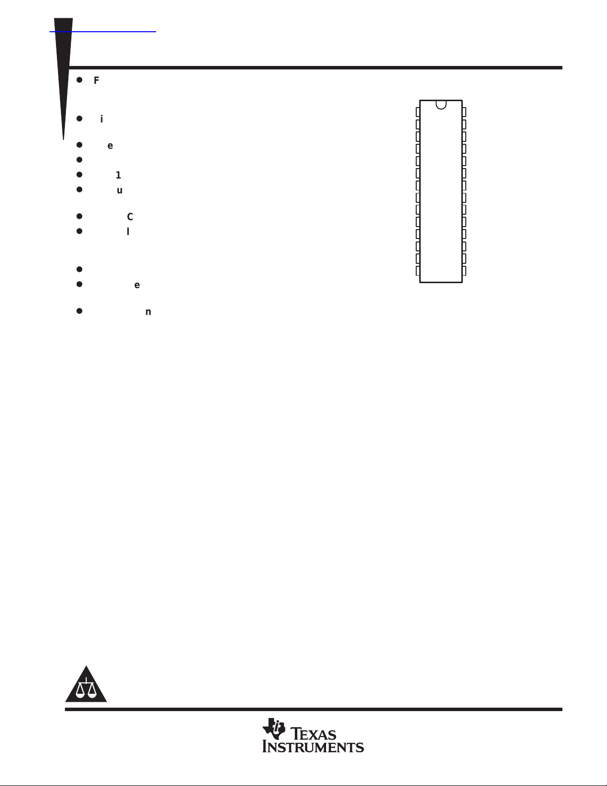
DW PACKAGE
(TOP VIEW)
1
28
2
27
3
26
4
25
5
24
6
23
7
22
8
21
9
20
10
19
11
18
12
17
13
16
14
15
REF0
REF1
V
CC
CLK12
CLK24
GND
BCLK2
BCLK3
V
CC
BCLK4
BCLK5
GND
BCLK1
BCLK0
D
Four CPU Clock Outputs With
Programmable Frequency
(50 MHz, 60 MHz, and 66 MHz)
D
Six Clock Outputs at Half-CPU Frequency
for PCI
D
One 24-MHz Clock Output
D
One 12-MHz Clock Output
D
Two 14.318-MHz Reference Outputs
D
All Output Clock Frequencies Derived From
a Single 14.31818-MHz Crystal Input
D
LVTTL-Compatible Inputs and Outputs
D
Internal Loop Filters for Phase-Lock Loops
Eliminate the Need for External
Components
D
Operates at 3.3 V
D
Distributed VCC and Ground Pins Reduce
CC
Switching Noise
D
Packaged in Plastic Small-Outline Package
description
The CDC9841 is a high-performance clock synthesizer/driver that generates all required clock signals
necessary for a high-performance PC motherboard. The four central processing unit (CPU) clock outputs
(PCLKn) are programmable to one of three frequencies (50 MHz, 60 MHz, or 66 MHz) via the SEL0 and SEL1
control inputs. The six peripheral-component-interconnect (PCI) clock outputs (BCLKn) are half the frequency
of PCLKn and are delayed 1 ns to 4 ns from the rising edge of the CPU clock. In addition, the four fixed-frequency
outputs provide a 24-MHz clock (CLK24), a 12-MHz clock (CLK12), and two buffered copies of the 14.318-MHz
input reference (REF0, REF1).
The CDC9841 generates all output frequencies from a 14.31818-MHz crystal input. A reference clock can be
provided at X1 instead of a crystal input.
Two phase-lock loops (PLLs) generate the CPU clock frequency and the 24-MHz clock frequency . On-chip loop
filters and internal feedback eliminate the need for external components. The PCI and 12-MHz clock
frequencies are derived from the base CPU and 24-MHz clock frequencies, respectively. The PLL circuit can
be bypassed in the TEST mode (i.e., SEL0 = SEL1 = H) to distribute a test clock provided at the X1 input.
Because the CDC9841 is based on PLL circuitry , it requires a stabilization time to achieve phase lock of the PLL.
This stabilization time is required following power up and application of a fixed-frequency, fixed-phase signal
at the X1 input, as well as following any changes to the SELn inputs.
PCLKn and BCLKn provide low-skew/low-jitter clock signals for reliable clock operation. All outputs are 3 state
and are enabled via OE.
Please be aware that an important notice concerning availability, standard warranty, and use in critical applications of
Texas Instruments semiconductor products and disclaimers thereto appears at the end of this data sheet.
PRODUCTION DATA information is current as of publication date.
Products conform to specifications per the terms of Texas Instruments
standard warranty. Production processing does not necessarily include
testing of all parameters.
Copyright 1996, Texas Instruments Incorporated
POST OFFICE BOX 655303 • DALLAS, TEXAS 75265
1
Page 2

CDC9841
PC MOTHERBOARD CLOCK SYNTHESIZER/DRIVER
WITH 3-STATE OUTPUTS
SCAS458D – DECEMBER 1994 – REVISED APRIL 1996
FUNCTION TABLE
OE
L X X 14.31818 MHz Hi-Z Hi-Z Hi-Z Hi-Z Hi-Z
H L L 14.31818 MHz 50 MHz 25 MHz 14.318 MHz 24 MHz 12 MHz
H L H 14.31818 MHz 60 MHz 30 MHz 14.318 MHz 24 MHz 12 MHz
H H L 14.31818 MHz 66 MHz 33 MHz 14.318 MHz 24 MHz 12 MHz
H H H TCLK
†
TCLK is a test clock input at the X1 input during test mode.
SEL0 SEL1 X1 PCLKn BCLKn REFn CLK24 CLK12
†
TCLK/2 TCLK/4 TCLK TCLK/4 TCLK/8
2
POST OFFICE BOX 655303 • DALLAS, TEXAS 75265
Page 3
functional block diagram
5
OE
3
X2
2
X1
OSC
CDC9841
PC MOTHERBOARD CLOCK SYNTHESIZER/DRIVER
WITH 3-STATE OUTPUTS
SCAS458D – DECEMBER 1994 – REVISED APRIL 1996
28
REF0
27
REF1
24
CLK24
SEL0
SEL1
13
12
Select
Logic
÷2
24-MHZ
PLL
CPU CLK
PLL
÷2
÷2
÷2
25
10
15
16
22
6
7
9
CLK12
PCLK0
PCLK1
PCLK2
PCLK3
BCLK0
BCLK1
BCLK2
POST OFFICE BOX 655303 • DALLAS, TEXAS 75265
21
19
18
BCLK3
BCLK4
BCLK5
3
Page 4

CDC9841
PC MOTHERBOARD CLOCK SYNTHESIZER/DRIVER
WITH 3-STATE OUTPUTS
SCAS458D – DECEMBER 1994 – REVISED APRIL 1996
absolute maximum ratings over operating free-air temperature range (unless otherwise noted)
†
Supply voltage range, VCC –0.5 V to 4.6 V. . . . . . . . . . . . . . . . . . . . . . . . . . . . . . . . . . . . . . . . . . . . . . . . . . . . . . . . .
Input voltage range, VI (see Note 1) –0.5 V to 4.6 V. . . . . . . . . . . . . . . . . . . . . . . . . . . . . . . . . . . . . . . . . . . . . . . . .
Voltage range applied to any output in the high state or power-off state,
V
(see Note 1) –0.5 V to VCC + 0.5 V. . . . . . . . . . . . . . . . . . . . . . . . . . . . . . . . . . . . . . . . . . . . . . . . . . . . . . . . . .
O
Current into any output in the low state, IO 2
Input clamp current, I
Output clamp current, I
Maximum power dissipation at T
Storage temperature range, T
†
Stresses beyond those listed under “absolute maximum ratings” may cause permanent damage to the device. These are stress ratings only, and
functional operation of the device at these or any other conditions beyond those indicated under “recommended operating conditions” is not
implied. Exposure to absolute-maximum-rated conditions for extended periods may affect device reliability.
NOTES: 1. The input and output negative-voltage ratings may be exceeded if the input and output clamp-current ratings are observed.
2. The maximum package power dissipation is calculated using a junction temperature of 150°C and a board trace length of 750 mils.
For more information, refer to the
Data Book
, literature number SCBD002B.
(V
< 0) –18 mA. . . . . . . . . . . . . . . . . . . . . . . . . . . . . . . . . . . . . . . . . . . . . . . . . . . . . . . . . . .
IK
I
(V
< 0) –50 mA. . . . . . . . . . . . . . . . . . . . . . . . . . . . . . . . . . . . . . . . . . . . . . . . . . . . . . . .
OK
O
= 55°C (in still air) (see Note 2) 1.2 W. . . . . . . . . . . . . . . . . . . . . . . . . . . . . . .
A
–65°C to 150°C. . . . . . . . . . . . . . . . . . . . . . . . . . . . . . . . . . . . . . . . . . . . . . . . . . .
stg
Package Thermal Considerations
. . . . . . . . . . . . . . . . . . . . . . . . . . . . . . . . . . . . . . . . . . . . .
application note in the 1994
ABT Advanced BiCMOS T echnology
I
OHmax
recommended operating conditions (see Note 3)
MIN MAX UNIT
V
CC
V
IH
V
IL
V
I
I
OH
I
OL
T
A
NOTE 3: Unused inputs must be held high or low to prevent them from floating.
Supply voltage 3.135 3.6 V
High-level input voltage 2 V
Low-level input voltage 0.8 V
Input voltage 0 V
REF0 –12
REF1 –8
High-level output current
Low-level output current
Operating free-air temperature 0 70 °C
PCLKn
BCLKn –12
CLK24, CLK12 –4
REF0 12
REF1 8
PCLKn
BCLKn 12
CLK24, CLK12 4
CC
–6
mA
mA
6
V
4
POST OFFICE BOX 655303 • DALLAS, TEXAS 75265
Page 5

OH
CC
I
mA
CLK24, CLK12
2.5
OL
CC
I
mA
CLK24, CLK12
0.4
I
CC
,
O
,
mA
‡
CDC9841
PC MOTHERBOARD CLOCK SYNTHESIZER/DRIVER
WITH 3-STATE OUTPUTS
SCAS458D – DECEMBER 1994 – REVISED APRIL 1996
electrical characteristics over recommended operating free-air temperature range (unless
otherwise noted)
PARAMETER TEST CONDITIONS MIN MAX UNIT
V
IK
V
OH
V
OL
I
I
I
OZ
CC
C
i
C
o
C
pd
†
Device in normal operating mode with no load on outputs
VCC = 3.135 V, II = –18 mA –1.2 V
IOH = –12 mA REF0 2.5
IOH = –8 mA REF1 2.5
VCC = 3.135 V
VCC = 3.135 V
VCC = 3.6 V, VI = VCC or GND ±1 µA
VCC = 3.6 V, VO = VCC or GND ±10 µA
V
= 3.6 V, I
VI = VCC or GND
VI = VCC or GND pF
VO = VCC or GND pF
VI = 3 V or 0 pF
IOH = –6 mA PCLKn 2.5
IOH = –12 mA BCLKn 2.5
= –4
OH
IOL = 12 mA REF0 0.4
IOL = 8 mA REF1 0.4
IOL = 6 mA PCLKn 0.4
IOL = 12 mA BCLKn 0.4
= 4
OL
= 0,
Outputs enabled
Outputs disabled 1
†
50
V
V
timing requirements over recommended ranges of supply voltage and operating free-air
temperature
MIN MAX UNIT
After SEL1, SEL0 5
Stabilization time
‡
Time required for the integrated PLL circuit to obtain phase lock of its feedback signal to its reference signal. In order for phase lock to be obtained,
a fixed-frequency, fixed-phase reference signal must be present at X1. Until phase lock is obtained, the specifications for propagation delay and
skew parameters given in the switching characteristics table are not applicable.
After OE↑ 5
After power up 5
ms
POST OFFICE BOX 655303 • DALLAS, TEXAS 75265
5
Page 6

CDC9841
()
()
†
ps
†
ps
t
ns
†‡
PCLKn (C
pF), BCLKn (C
pF)
2
ns
t
†‡
PCLKn (C
BCLKn (C
F)
2
ns
PC MOTHERBOARD CLOCK SYNTHESIZER/DRIVER
WITH 3-STATE OUTPUTS
SCAS458D – DECEMBER 1994 – REVISED APRIL 1996
switching characteristics (see Figures 1 and 2)
PARAMETER
t
skew
†
Offset
Jitter
Duty cycle
c
t
r
f
†
Specifications are applicable only after the PLL stabilization time has elapsed.
‡
Rise and fall times are characterized using the load circuits shown in Figure 1.
†
FROM
(INPUT)
PCLKn (CL = 20 pF)
(OUTPUT)
PCLKn (CL = 20 pF) 200
BCLKn (CL = 30 pF) 400
BCLKn (CL = 30 pF) 1 4 ns
PCLKn (CL = 20 pF) ±250
BCLKn (CL = 30 pF) ±350
Any output
PCLKn (CL = 20 pF)
BCLKn (CL = 30 pF)
p
= 20
L
p
= 20 pF),
L
TO
SEL0 = L, SEL1 = L
SEL0 = L, SEL1 = H
SEL0 = H, SEL1 = L
SEL0 = L, SEL1 = L
SEL0 = L, SEL1 = H
SEL0 = H, SEL1 = L
= 30
L
= 30 p
L
VCC = 3.135 V
to 3.6 V,
TA = 0°C to 70°C
MIN MAX
45% 55%
20
16.7
15
40
33.3
30
p
p
UNIT
p
p
6
POST OFFICE BOX 655303 • DALLAS, TEXAS 75265
Page 7

CDC9841
PC MOTHERBOARD CLOCK SYNTHESIZER/DRIVER
WITH 3-STATE OUTPUTS
SCAS458D – DECEMBER 1994 – REVISED APRIL 1996
PARAMETER MEASUREMENT INFORMATION
CLOCK DRIVER CIRCUITS
t
From Output
Under Test
(see Note A)
C
L
LOAD CIRCUIT
500 Ω
2.4 V
1.5 V
0.4 V
t
r
VOLTAGE WAVEFORMS
c
Duty Cycle
t
f
NOTES: A. CL includes probe and jig capacitance.
B. The outputs are measured one at a time with one transition per measurement.
Figure 1. Load Circuit and Voltage Waveforms
CPU Clock
(PCLK)
CPU Clock
(PCLK)
skew
PCI Clock
(BCLK)
PCI Clock
(BCLK)
skew
CPU Clock
(PCLK)
PCI Clock
(BCLK)
offset
1.5 V
PCLK-to-PCLK Skew
1.5 V
BCLK-to-BCLK Skew
1.5 V
offset
1.5 V
1.5 V
1.5 V
V
OH
GND
V
OH
GND
V
OH
GND
V
OH
GND
V
OH
GND
V
OH
GND
PCLK-to-BCLK Offset
Figure 2. Waveforms for Calculation of t
POST OFFICE BOX 655303 • DALLAS, TEXAS 75265
skew
and Offset
7
Page 8

IMPORTANT NOTICE
T exas Instruments and its subsidiaries (TI) reserve the right to make changes to their products or to discontinue
any product or service without notice, and advise customers to obtain the latest version of relevant information
to verify, before placing orders, that information being relied on is current and complete. All products are sold
subject to the terms and conditions of sale supplied at the time of order acknowledgement, including those
pertaining to warranty, patent infringement, and limitation of liability.
TI warrants performance of its semiconductor products to the specifications applicable at the time of sale in
accordance with TI’s standard warranty. Testing and other quality control techniques are utilized to the extent
TI deems necessary to support this warranty . Specific testing of all parameters of each device is not necessarily
performed, except those mandated by government requirements.
CERTAIN APPLICA TIONS USING SEMICONDUCT OR PRODUCTS MAY INVOLVE POTENTIAL RISKS OF
DEATH, PERSONAL INJURY, OR SEVERE PROPERTY OR ENVIRONMENTAL DAMAGE (“CRITICAL
APPLICATIONS”). TI SEMICONDUCTOR PRODUCTS ARE NOT DESIGNED, AUTHORIZED, OR
WARRANTED TO BE SUITABLE FOR USE IN LIFE-SUPPORT DEVICES OR SYSTEMS OR OTHER
CRITICAL APPLICA TIONS. INCLUSION OF TI PRODUCTS IN SUCH APPLICATIONS IS UNDERST OOD TO
BE FULLY AT THE CUSTOMER’S RISK.
In order to minimize risks associated with the customer’s applications, adequate design and operating
safeguards must be provided by the customer to minimize inherent or procedural hazards.
TI assumes no liability for applications assistance or customer product design. TI does not warrant or represent
that any license, either express or implied, is granted under any patent right, copyright, mask work right, or other
intellectual property right of TI covering or relating to any combination, machine, or process in which such
semiconductor products or services might be or are used. TI’s publication of information regarding any third
party’s products or services does not constitute TI’s approval, warranty or endorsement thereof.
Copyright 1998, Texas Instruments Incorporated
 Loading...