

Page 1
查询CDC930供应商
133-MHz DIFFERENTIAL CLOCK SYNTHESIZER/DRIVER FOR PC MOTHERBOARDS
CDC930
WITH 3-STATE OUTPUTS
SCAS641 – JUL Y 2000
D
Generates Clocks for Pentium4
Microprocessors
D
Uses a 14.318 MHz Crystal Input to
Generate Multiple Output Frequencies
D
Includes Spread Spectrum Clocking (SSC),
0.6% Downspread for Reduced EMI With
Theoretical EMI Damping of 7 dB
D
Power Management Control Terminals
D
Low Output Skew and Jitter for Clock
Distribution
D
Operates From Single 3.3-V Supply
D
Consumes Less Than 30-mA Power-Down
Current
D
Generates the Following Clocks:
– 4 HCLK (Host) (Different Pairs–
100/133 MHz)
– 1 3VMREF Pair (3.3 V, 180° Shifted
50/66 MHz)
– 10 PCI (3.3 V, 33.3 MHz)
– 2 REF (3.3 V, 14.318 MHz)
– 4 3V66 MHz (3.3 V, 66 MHz)
– 2 3V48 MHz (3.3 V, 48 MHz)
D
Packaged in 56-Pin SSOP Package
description
The CDC930 is a differential clock synthesizer/
driver that generates HCLK/HCLK, 3VMREF/
3VMREF, PCI, 3V66, 3V48, REF system clock
signals to support a computer system with a
Pentium4 microprocessor and a Direct
Rambus memory subsystem.
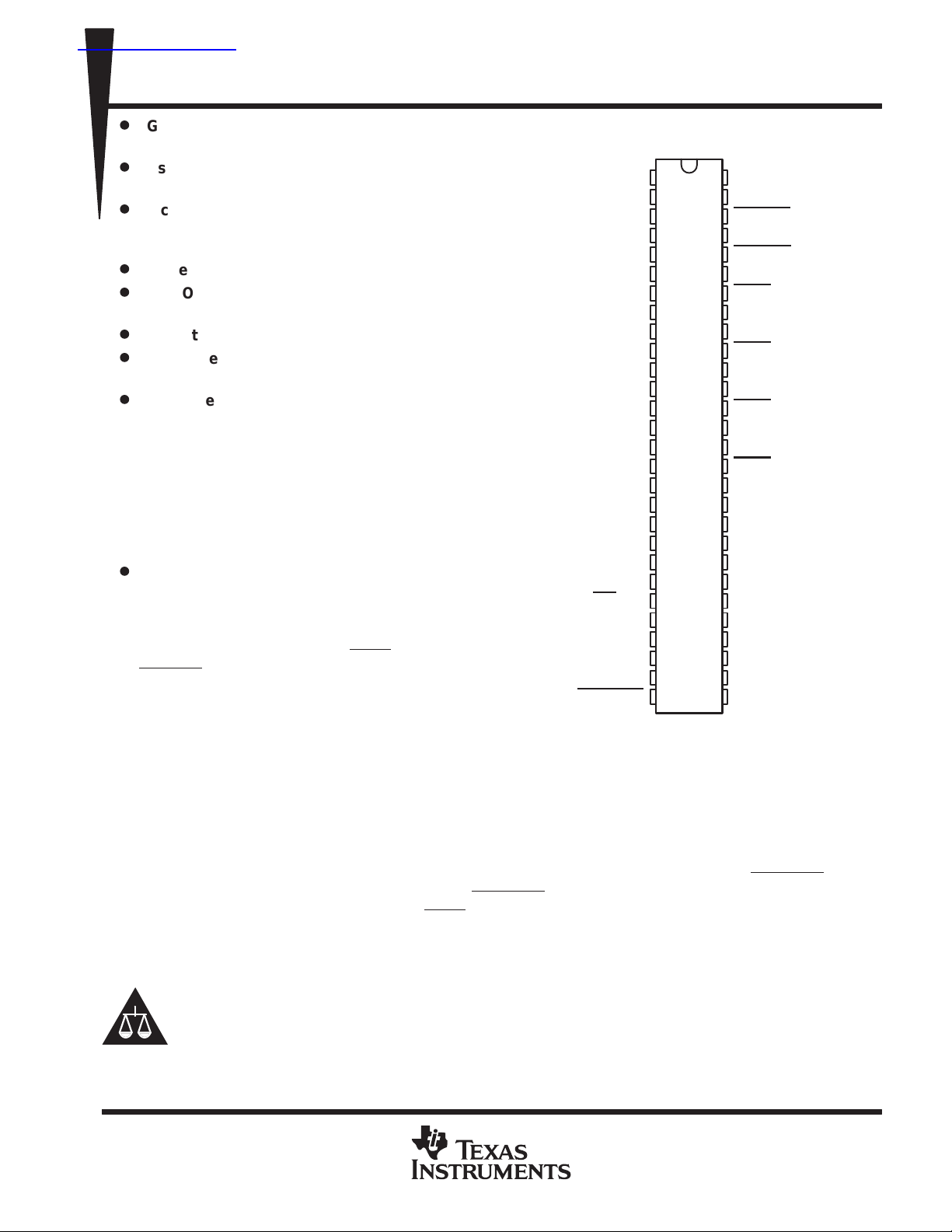
DL PACKAGE
(TOP VIEW)
GND
REF0/MultSel0
REF1/MultSel1
V
3.3V
†
DD
XOUT
GND
PCI0
PCI1
V
3.3V
DD
PCI2
PCI3
GND
PCI4
PCI5
V
3.3V
DD
PCI6
PCI7
GND
PCI8
PCI9
V
3.3V
DD
SEL100
GND
3V48(0)/SelA
3V48(1)/SelB
V
3.3V
DD
PWRDWN
XIN
/133
1
2
3
4
5
6
7
8
9
10
11
12
13
14
15
16
17
18
19
20
21
22
23
24
25
26
27
28
56
55
54
53
52
51
50
49
48
47
46
45
44
43
42
41
40
39
38
37
36
35
34
33
32
31
30
29
VDD3.3V
3VMREF
3VMREF
GND
SPREAD
HCLK(1)
HCLK
(1)
V
3.3V
DD
HCLK(2)
HCLK
(2)
GND
HCLK(3)
HCLK
(3)
V
3.3V
DD
HCLK(4)
HCLK
(4)
GND
I_REF
3.3V
V
DD
GND
V
3.3V
DD
3V66(0)
3V66(1)
GND
GND
3V66(2)
3V66(3)
V
3.3V
DD
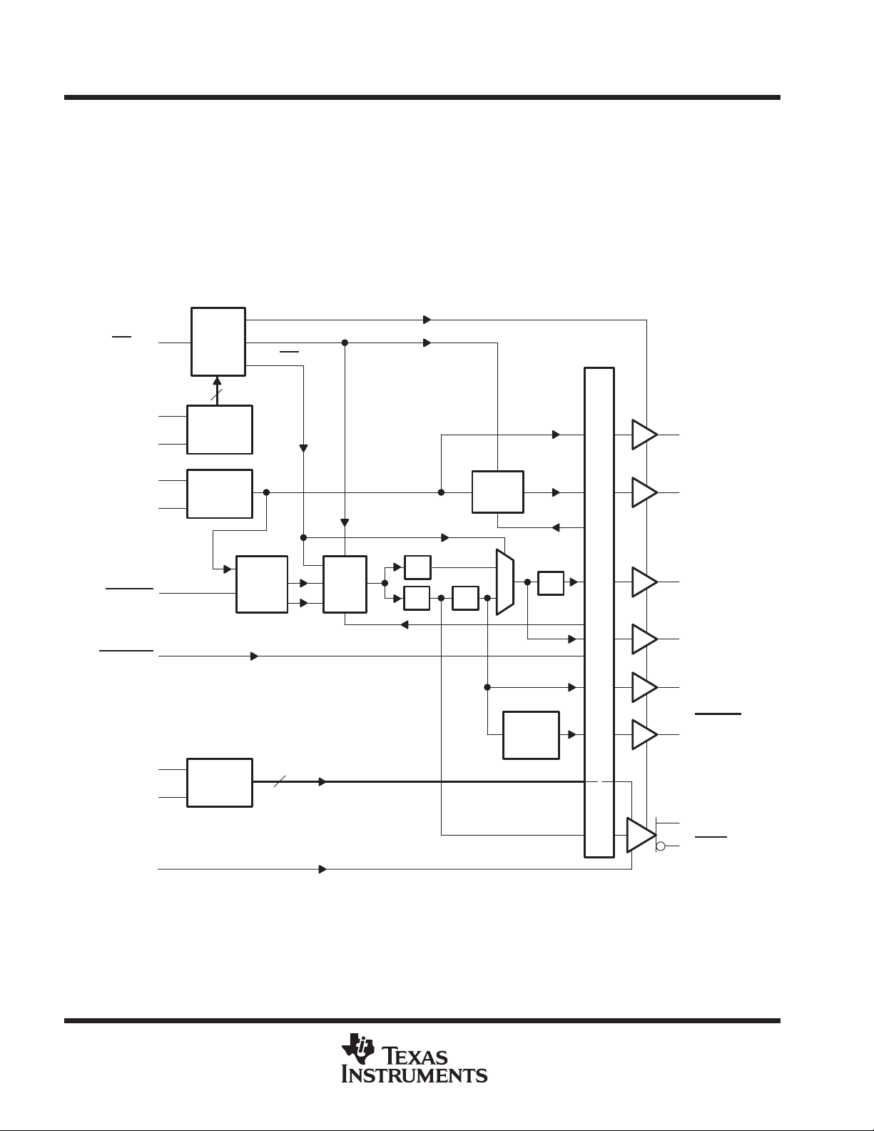
All output frequencies are generated from a 14.318-MHz crystal input. A reference clock input can be provided
at the XIN input instead of a crystal. Two phase-locked loops (PLLs) are used to generate the host frequencies
and the 48-MHz clock frequencies. On-chip loop filters and internal feedback eliminate the need for external
components. The host, PCI clock and 48-MHz clock outputs provide low-skew/low-jitter clock signals for reliable
clock operation. All outputs have 3-state capability , which can be selected using control inputs SEL133, SelA
and SelB.
The outputs are either differential host clock or 3.3-V single-ended CMOS buffers. When PWRDWN
high, the device operates in normal mode. When PWRDWN is set low, the device transitions to a power-down
mode in which HCLK is driven at 2×I
Please be aware that an important notice concerning availability, standard warranty, and use in critical applications of
Texas Instruments semiconductor products and disclaimers thereto appears at the end of this data sheet.
†
This is system design dependant.
Intel and Pentium4 are trademarks of Intel Corporation.
Rambus is a trademark of Rambus Corporation.
PRODUCTION DATA information is current as of publication date.
Products conform to specifications per the terms of Texas Instruments
standard warranty. Production processing does not necessarily include
testing of all parameters.
, HCLK is not driven, and all others are set low.
REF
Copyright 2000, Texas Instruments Incorporated
POST OFFICE BOX 655303 • DALLAS, TEXAS 75265
is set to
1
Page 2
CDC930
133-MHz DIFFERENTIAL CLOCK SYNTHESIZER/DRIVER FOR PC MOTHERBOARDS
WITH 3-STATE OUTPUTS
SCAS641 – JUL Y 2000
description (continued)
The HOST bus operates at 100 MHz or 133 MHz. The MREF bus operates at 50 MHz or 66 MHz. Output
frequency selection is accomplished with corresponding setting for SEL100/133 control input. The PCI bus
frequency is fixed to 33 MHz.
Since the CDC930 is based on PLL circuitry, it requires a stabilization time to achieve phase-lock of the PLL.
This stabilization time is required following power up as well as changes to SEL inputs. With use of external
reference clock, this signal must be fixed-frequency and fixed-phase prior stabilization time starts.
functional block diagram
3-State/Low
SEL100/133
SELA
SELB
23
25
26
Control
Logic
2
Latched
Test
SEL 100
/133
2*REF
14.318 MHz
(2,3)
XIN
XOUT
SPREAD
PWRDWN
MultSel0
MultSel1
I_REF
5
6
52
28
2
3
39
Xtal
Oscillator
Latched
Spread
Logic
48 MHz
PLL
CPU
PLL
2
/3
/2
/2
/2
Sync Logic and Power Down Logic
180°
Phase
Shift
2*3V48
48 MHz
(25,26)
10*PCI
33 MHz
(8,9,11,12,14,
15,17,18,20,21)
4*3V66
66 MHz
(30,31,34,35)
1*3VMREF
50/66 MHz
(55)
1*3VMREF
50/66 MHz
(54)
4*HCLK
100/133 MHz
(42,45,48,51)
4*HCLK
100/133 MHz
(41,44,47,50)
2
POST OFFICE BOX 655303 • DALLAS, TEXAS 75265
Page 3
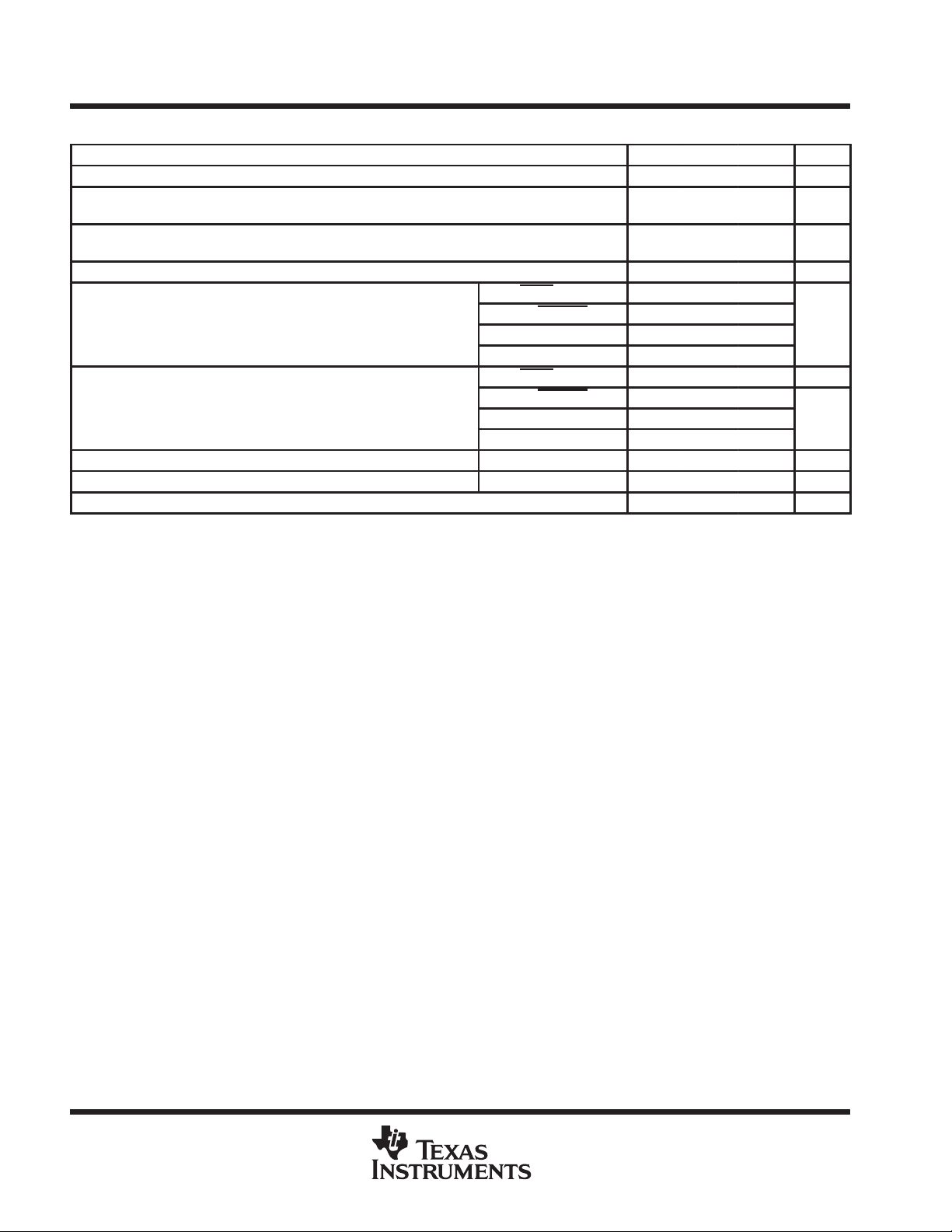
I/O
DESCRIPTION
CDC930
133-MHz DIFFERENTIAL CLOCK SYNTHESIZER/DRIVER FOR PC MOTHERBOARDS
WITH 3-STATE OUTPUTS
SCAS641 – JUL Y 2000
Terminal Functions
TERMINAL
NAME NO.
3V48(0)/SelA 25 I/O Dual function 3.3 V , Type 3, 48-MHz clock output that latches the state of SelA during power up
3V48(1)/SelB 26 I/O Dual function 3.3 V , Type 3, 48-MHz clock output that latches the state of SelB during power up
3V66[0–3] 30, 31, 34, 35 O 3.3 V, Type 5, 66-MHz clock outputs
3VMREF 55 O 3.3 V, Type 5, 50/66-MHz memory clock output
3VMREF 54 O 3.3 V, Type 5, 50/66-MHz memory clock output (180° out of phase with 3VMREF)
GND 1, 7, 13, 19,
24, 32, 33, 37,
40, 46, 53
HCLK[1–4] 42, 45, 48, 51 O Type X1, host clock outputs
HCLK[1–4] 41, 44, 47, 50 O Type X1, host complementary clock outputs
I_REF 39 Special Current reference pin for the host clock pairs. I_REF uses a fixed precision resistor tied to ground
PCI[0–9] 8, 9, 11, 12,
14, 15, 17, 18,
20, 21
PWRDWN 28 I Power down for complete device with HOST at 2×I
REF0/MultSel0 2 I/O Dual function 3.3 V, Type 3, 14.318-MHz reference clock output. The state of MultSel0 is latched
REF1/MultSel1 3 I/O Dual function 3.3 V, Type 3, 14.318-MHz reference clock output. The state of MultSel1 is latched
SEL100/133 23 I Active low LVTTL level logic select. SEL100/133 is used for enabling 100/133 MHz. Low=100
SPREAD 52 I LVTTL level logic select. SPREAD pin enables/disables the spread spectrum for the
VDD3.3V 4, 10, 16, 22,
27, 29, 36, 38,
43, 49, 56
XIN 5 I Crystal input – 14.318 MHz
XOUT 6 O Crystal output – 14.318 MHz
Ground for core and HCLK/HCLK, 3VMREF/3VMREF, 3V48, 3V66 and PCI outputs
to establish the appropriate current.
O 3.3 V, Type 5, 33-MHz PCI clock outputs
, HCLK not driven and all other outputs
forced low.
during power up. MultSel0 configures the IOH amplitude (and thus the VOH swing amplitude) of
the HCLK pair outputs.
during power up. MultSel1 configures the IOH amplitude (and thus the VOH swing amplitude) of
the HCLK pair outputs.
MHz, high=133 MHz
HCLK/HCLK
I 3.3-V power for core and the HCLK/HCLK, 3VMREF/3VMREF, 3V48, 3V66, and PCI outputs.
, 3VMREF/3VMREF, 3V66 and PCI outputs.
REF
POST OFFICE BOX 655303 • DALLAS, TEXAS 75265
3
Page 4
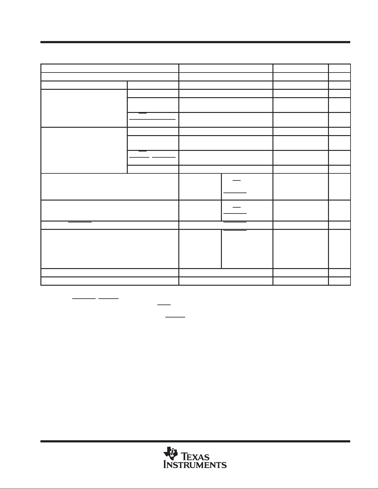
CDC930
FUNCTION
SPREAD
,
BOARD TARGET
REFERENCE R,
OUTPUT CURRENT
V
OH
Z
133-MHz DIFFERENTIAL CLOCK SYNTHESIZER/DRIVER FOR PC MOTHERBOARDS
WITH 3-STATE OUTPUTS
SCAS641 – JUL Y 2000
Function Tables
SELECT FUNCTIONS
INPUTS
SEL100/133 SelA SelB HOST, HCLK 3VMREF, 3VMREF PCI 3V66 3V48 REF
0 0 0 100 MHz 50 MHz 33 MHz 66 MHz 48 MHz 14.318 MHz Active 100 MHz
0 1 1 Hi-Z Hi-Z Hi-Z Hi-Z Hi-Z Hi-Z All outputs 3-stated
1 0 0 133 MHz 66 MHz 33 MHz 66 MHz 48 MHz 14.318 MHz Active 133 MHz
1 1 1 TCLK/2 TCLK/4 TCLK/8 TCLK/4 TCLK/2 TCLK Test Mode
ENABLE FUNCTION
INPUT
SEL100/133 HCLK HCLK 3VMREF, 3VMREF PCI 3V66 3V48 REF
0 2×I
1 On On On On On On On
INPUT
0 Spread spectrum clocking active, –0.6% at HCLK/HCLK, 3VMREF/3VMREF, 3V66, PCI
1 Spread spectrum clocking nonactive
Not driven L L L L L
REF
SPREAD SPECTRUM FUNCTION
OUTPUTS
OUTPUTS
OUTPUTS
OUTPUT BUFFER SPECIFICATIONS
BUFFER NAME
3V48, REF 3.135 – 3.465 20–60 TYPE 3
PCI, 3V66 3.135 – 3.465 12–65 TYPE 5
3VMREF/3VMREF 3.135 – 3.465 12–55 TYPE 5
HCLK/HCLK TYPE X1
INPUTS
MultSel0 MultSel1
0 0 60 Ω Rr = 475 1%, I
0 0 50 Ω Rr = 475 1%, I
0 1 60 Ω Rr = 475 1%, I
0 1 50 Ω Rr = 475 1%, I
1 0 60 Ω Rr = 475 1%, I
1 0 50 Ω Rr = 475 1%, I
1 1 60 Ω Rr = 475 1%, I
1 1 50 Ω Rr = 475 1%, I
NOTE: The entries in boldface are the primary system configurations of interest. The outputs should be optimized for these configurations
BOARD TARGET REFERENCE R
TRACE/TERM Z
VDD RANGE
(V)
OUTPUT BUFFER SPECIFICATIONS
I
REF
IMPEDANCE
(Ω)
= VDD/3×Rr)
= 2.32 mA IOH = 5×I
REF
= 2.32 mA IOH = 5×I
REF
= 2.32 mA IOH = 6×I
REF
= 2.32 mA IOH = 6×I
REF
= 2.32 mA IOH = 4×I
REF
= 2.32 mA IOH = 4×I
REF
= 2.32 mA IOH = 7×I
REF
= 2.32 mA IOH = 7×I
REF
BUFFER TYPE
REF
REF
REF
REF
REF
REF
REF
REF
V
AT Z
AT
IREF = 2.32 mA
0.71 V at 60 Ω
0.59 V at 50 Ω
0.85 V at 60 Ω
0.71 V at 50 Ω
0.56 V at 60 Ω
0.47 V at 50 Ω
0.99 V at 60 Ω
0.82 V at 50 Ω
4
POST OFFICE BOX 655303 • DALLAS, TEXAS 75265
Page 5
‡
PACKAGE
A
A
A
CDC930
133-MHz DIFFERENTIAL CLOCK SYNTHESIZER/DRIVER FOR PC MOTHERBOARDS
WITH 3-STATE OUTPUTS
SCAS641 – JUL Y 2000
absolute maximum ratings over operating free-air temperature (unless otherwise noted)
†
Supply voltage range, VDD –0.5 V to 4.6 V. . . . . . . . . . . . . . . . . . . . . . . . . . . . . . . . . . . . . . . . . . . . . . . . . . . . . . . . .
Input voltage range, VI (see Note 1) –0.5 V to VDD + 0.5 V. . . . . . . . . . . . . . . . . . . . . . . . . . . . . . . . . . . . . . . . . . .
Voltage range applied to any output in the high-impedance state or power-off state,
V
Current into any output in the low state, IO 2× rated I
(see Note 1) –0.5 V to VDD + 0.5 V. . . . . . . . . . . . . . . . . . . . . . . . . . . . . . . . . . . . . . . . . . . . . . . . . . . . . . . .
O
. . . . . . . . . . . . . . . . . . . . . . . . . . . . . . . . . . . . . . . . . . . . .
Input clamp current, IIK (VI < 0) –18 mA. . . . . . . . . . . . . . . . . . . . . . . . . . . . . . . . . . . . . . . . . . . . . . . . . . . . . . . . . .
(VI < VDD) 18 mA. . . . . . . . . . . . . . . . . . . . . . . . . . . . . . . . . . . . . . . . . . . . . . . . . . . . . . . .
Output clamp current , IOK (VO < 0) –50 mA. . . . . . . . . . . . . . . . . . . . . . . . . . . . . . . . . . . . . . . . . . . . . . . . . . . . . . .
(VO < VDD) 50 mA. . . . . . . . . . . . . . . . . . . . . . . . . . . . . . . . . . . . . . . . . . . . . . . . . . . . . . .
Package thermal impedance, θJA (see Note 2) 74°C/W. . . . . . . . . . . . . . . . . . . . . . . . . . . . . . . . . . . . . . . . . . . . .
Maximum power dissipation at TA = 55°C (in still air) (see Note 3) 1.3 W. . . . . . . . . . . . . . . . . . . . . . . . . . . . . . .
Operating free-air temperature range, T
Storage temperature range, T
–65°C to 150°C. . . . . . . . . . . . . . . . . . . . . . . . . . . . . . . . . . . . . . . . . . . . . . . . . . .
stg
0°C to 85°C. . . . . . . . . . . . . . . . . . . . . . . . . . . . . . . . . . . . . . . . . . . . . .
A
Lead temperature 1,6 mm (1/16 inch) from case for 10 seconds 260°C. . . . . . . . . . . . . . . . . . . . . . . . . . . . . . .
†
Stresses beyond those listed under “absolute maximum ratings” may cause permanent damage to the device. These are stress ratings only, and
functional operation of the device at these or any other conditions beyond those indicated under “recommended operating conditions” is not
implied. Exposure to absolute-maximum-rated conditions for extended periods may affect device reliability.
NOTES: 1. The input and output negative-voltage ratings may be exceeded if the input and output clamp-current ratings are observed.
2. The package thermal impedance is calculated in accordance with EIA/JEDEC Std JESD51, except for the through-hole packages,
which use a trace length of zero. The absolute maximum power dissipation allowed at TA = 55°C (in still air) is 1.3 W.
3. The maximum package power dissipation is calculated using a junction temperature of 1505C and a board trace length of 750 mils.
For more information, refer to the
Book
, literature number SCBD002.
Package Thermal Considerations
application note in the
ABT Advanced BiCMOS T echnology Data
OL
DISSIPATION RATING TABLE
T
≤ 25°C DERATING FACTOR
POWER RATING ABOVE TA = 25°C
DL 1558.6 mW 12.468 mW/°C 997.5 mW 810.52 mW
‡
This is the inverse of the traditional junction-to-case thermal resistance (R
at 74°C/W.
T
= 70°C T
POWER RATING
) and uses a board-mounted device
θJA
= 85°C
POWER RATING
POST OFFICE BOX 655303 • DALLAS, TEXAS 75265
5
Page 6
CDC930
High-level output current, I
mA
Low-level output current, I
133-MHz DIFFERENTIAL CLOCK SYNTHESIZER/DRIVER FOR PC MOTHERBOARDS
WITH 3-STATE OUTPUTS
SCAS641 – JUL Y 2000
recommended operating conditions (see Note 2)
MIN NOM
Supply voltage, V
High-level input voltage, V
Low-level input voltage, V
Input voltage, V
Reference frequency, f
Crystal frequency, f
Operating free-air temperature, T
†
All nominal values are measured at their respective nominal VDD values.
‡
Reference frequency is a test clock driven on the XIN input during the device test mode and normal mode. In test mode, XIN can be driven
externally up to f
§
This is a series fundamental crystal with fO = 14.31818 MHz.
NOTES: 4. Unused inputs must be held high or low to prevent them from floating.
DD
IH
IL
I
p
p
(XIN)
5. VIH, VIL: All input levels referenced to VDD = 3.30 V.
OH
OL
‡
(XIN)
§
(XTAL)
A
= 16 MHz. If XIN is driven externally, XOUT is floating.
HCLK/HCLK –20
3VMREF/3VMREF –15
48MHz, REFx –16
PCIx, 3V66x –15
HCLK/HCLK 5 µA
3VMREF/3VMREF 10
48MHz, REFx 10
PCIx, 3V66x 10
Test mode 14 MHz
Normal mode 13.8 14.318 14.8 MHz
3.135 3.465 V
2
GND –
0.3 V
0 V
0 85 °C
†
VDD +
MAX UNIT
0.3 V
0.8 V
DD
V
V
mA
6
POST OFFICE BOX 655303 • DALLAS, TEXAS 75265
Page 7
IILLow-level input current
CDC930
133-MHz DIFFERENTIAL CLOCK SYNTHESIZER/DRIVER FOR PC MOTHERBOARDS
WITH 3-STATE OUTPUTS
SCAS641 – JUL Y 2000
electrical characteristics over recommended operating free-air temperature range (unless
otherwise noted)
PARAMETER TEST CONDITIONS MIN TYP†MAX UNIT
V
IK
R
I
I
IH
I
OZ
I
DD(Z)
I
DD(PD)
I
DD
C
I
C
(XTAL)
†
All typical values are measured at their respective nominal VDD values.
‡
These parameters are ensured by design and lab characterization, not 100% production tested.
Control SELx, PWRDWN
CL = MAX = 5 pF, Rs = 33.2 Ω, Rp = 49.9 Ω at HCLK/HCLK
CL = MAX = 20 pF, RL = 500 Ω at 48 MHz, REF (Type 3)
CL = MAX = 30 pF, RL = 500 Ω at PCIx, 3V66, 3VMREF, 3VMREF
Input clamp voltage VDD = 3.135 V, II = –18 mA –1.2 V
Input resistance XIN-XOUT VDD = 3.465 V, VI = VDD –0.5 V 100 kΩ
XOUT VDD = 3.135 V, VI = VDD –0.5 V 50 mA
MultSel0, MultSel1,
High-level input current
p
High-impedance-state output current VDD = 3.465 V
High-impedance-state supply current VDD = 3.465 V
PWRDWN state supply current VDD = 3.465 V, PWRDWN = L 30 mA
Dynamic supply current VDD = 3.465 V
Input capacitance
Crystal terminal capacitance VDD = 3.3 V, VI = 0.3 V 18 pF
‡
, SPREAD threshold levels during FUNC w/c level tests.
SelA, SelB
SEL100/133
SPREAD, PWRDWN
XOUT VDD = 3.135 V, VO = 0 V –5 mA
MultSel0, MultSel1,
SelA, SelB,
SEL100/133
SPREAD
I_REF VDD = 3.465 V, Rr = 221 –5.5 mA
, PWRDWN
VDD = 3.465 V, VI = V
VDD = 3.465 V, VI = V
VDD = 3.465 V, VI = GND –10 µA
VDD = 3.465 V, VI = GND –5 µA
VDD = 3.3 V, VI = VDD or GND 2 5 pF
(Type X1)
(Type 5)
DD
DD
SELA, SELB = H,
SEL100
/133 H → L
VO = VDD or GND
PWRDWN
SELA, SELB = H,
SEL100
PWRDWN
PWRDWN = H,
HCLK = 133 MHz,
SSC = ON/OFF,
CL = MAX
R
ref
I
OUT
= H
/133 H → L
= H
= 475 Ω,
= 6 × I
ref
10 µA
5 µA
±10 µA
40 mA
250 mA
POST OFFICE BOX 655303 • DALLAS, TEXAS 75265
7
Page 8

CDC930
I
4
mA
I
5
mA
IOHHigh-level output current
V
Ω
I
6
mA
I
7
mA
OH
gg
VOLLow-level output voltage
V
OH
gg
VOLLow-level output voltage
V
133-MHz DIFFERENTIAL CLOCK SYNTHESIZER/DRIVER FOR PC MOTHERBOARDS
WITH 3-STATE OUTPUTS
SCAS641 – JUL Y 2000
electrical characteristics over recommended operating free-air temperature range (unless
otherwise noted) (continued)
HCLK/HCLK (Type X1)
PARAMETER TEST CONDITIONS MIN TYP†MAX UNIT
= 2.32 mA ×
ref
= 2.32 mA ×
ref
p
= 2.32 mA ×
ref
= 2.32 mA ×
ref
C
Output capacitance
O
†
All typical values are measured at their respective nominal VDD values.
‡
These parameters are ensured by design and lab characterization, not 100% production tested.
‡
VO = VDD or GND 3.5 pF
48MHz, REFx (Type 3), CL = 20 pF, RL = 500 Ω
PARAMETER TEST CONDITIONS MIN TYP†MAX UNIT
V
High-level output voltage
p
I
High-level output current
OH
I
Low-level output current
OL
C
Output capacitance
O
†
All typical values are measured at their respective nominal VDD values.
‡
These parameters are ensured by design and lab characterization, not 100% production tested.
‡
VDD = 3.135 V –8.1
VDD = 3.465 V –10.5
VDD = 3.135 V –10.1
VDD = 3.465 V
VDD = 3.135 V
VDD = 3.465 V –15.7
VDD = 3.135 V –14.1
VDD = 3.465 V –18.4
VDD = min to max, IOH = –1 mA
VDD = 3.135 V, IOH = –14 mA 2.4
VDD = min to max, IOL = 1 mA 0.1
VDD = 3.135 V, IOL = 9 mA 0.4
VDD = 3.135 V, VO = 1 V –29
VDD = 3.3 V,
VDD = 3.465 V, VO = 3.135 V –23
VDD = 3.135 V, VO = 1.95 V 29
VDD = 3.3 V,
VDD = 3.465 V, VO = 0.4 V 27
VDD = 3.3 V, VO = VDD or GND 2 5 pF
at Z = 50
OH
VO = 1.65 V –41
VO = 1.65 V 53
–12.1
VDD –
0.1 V
–13.1
mA
mA
V
PCIx, 3V66x, MREF/MREF (Type 5), CL = 20 pF, RL = 500 Ω
PARAMETER TEST CONDITIONS MIN TYP†MAX UNIT
V
High-level output voltage
p
I
High-level output current
OH
I
Low-level output current
OL
C
Output capacitance
O
†
All typical values are measured at their respective nominal VDD values.
‡
These parameters are ensured by design and lab characterization, not 100% production tested.
8
VDD = min to max, IOH = –1 mA
VDD = 3.135 V, IOH = –18 mA 2.4
VDD = min to max, IOL = 1 mA 0.1
VDD = 3.135 V, IOL = 12 mA 0.4
VDD = 3.135 V, VO = 1 V –33
VDD = 3.3 V,
VDD = 3.465 V, VO = 3.135 V –33
VDD = 3.135 V, VO = 1.95 V 30
VDD = 3.3 V,
VDD = 3.465 V, VO = 0.4 V 38
‡
POST OFFICE BOX 655303 • DALLAS, TEXAS 75265
VDD = 3.3 V, VO = VDD or GND 2 5 pF
VO = 1.65 V –53
VO = 1.65 V 70
VDD –
0.1 V
V
mA
mA
Page 9

mV
,
L
V
,,
SEL100/133
,,
,,
SEL100/133
,
,,
t
HCLK clock
d
†
ns
twPulse duration width
ns
am litude
CDC930
133-MHz DIFFERENTIAL CLOCK SYNTHESIZER/DRIVER FOR PC MOTHERBOARDS
WITH 3-STATE OUTPUTS
SCAS641 – JUL Y 2000
switching characteristics, VDD = MIN to MAX, TA = 0°C to 85°C
PARAMETER
v
v
v
v
t
PZL
t
PZH
t
PHZ
t
PLZ
t
PZL
t
PZH
t
PHZ
t
PLZ
t
stab
†
Stabilization time is the time required for the integrated PLL circuit to obtain phase lock of its feedback signal to its reference signal. In order for
phase lock to be obtained, a fixed-frequency, fixed-phase reference signal must be present a XIN. Until phase lock is obtained, the specifications
for propagation delay and skew parameters given in the switching characteristics tables are not applicable. Stabilization time is defined as the
time from when VDD achieves its nominal operating level until the output frequency is stable and operating within specification.
‡
These parameters are ensured by design and lab characterization, not 100% production tested.
Overshoot
over
Undershoot
under
Overshoot
over
Undershoot
under
Output enable time to low
level
Output enable time to high
level
Output disable time from
high level
Output disable time from low
level
Output enable time to low
level
Output enable time to high
level
Output disable time from
high level
Output disable time from low
level
Stabilization time
‡
‡
‡
‡
†
FROM
(INPUT)TO(OUTPUT)
HCLK/
HCLK
REF, 3V48
3VMREF,
3VMREF,
3V66, PCI
TEST CONDITIONS MIN TYP MAX UNIT
HCLK/HCLK 0.7 V amplitude
Other clocks, C
case
f
= 100 or 133 MHz,
(HCL)
SELA, SELB = H,
SEL100/133 L → H,
R
= 475 Ω
ref
f
= 100 or 133 MHz,
(HCL)
SELA, SELB = H,
SEL100/133 H → L,
R
= 475 Ω
ref
f
= 100 or 133 MHz,
(HCL)
SELA, SELB = H,
SEL100/133 L → H,
R
= 475 Ω
ref
f
= 100 or 133 MHz,
(HCL)
SELA, SELB = H,
SEL100/133 H → L,
R
= 475 Ω
ref
After power up 3 ms
= Worst
GND–0.7
VOH+200
VOL–200
VDD+0.7
100 ns
100 ns
10 ns
10 ns
10 ns
10 ns
10 ns
10 ns
HCLK/HCLK (Type X1) CL = 2 pF, RL > 500 kΩ
PARAMETER
c
t
jit(cc)
t
dc
t
sk(o)
t
r
t
f
tr, t
v
†
The average over any 1–µs period of time is greater than the minimum specified period.
‡
These parameters are ensured by design and lab characterization, not 100% production tested.
Cycle to cycle jitter f
Duty cycle
HCLK bus skew HCLKx HCLKx
Rise time‡
Fall time‡
Rise and fall time matching
f
Cross point voltages
cross
perio
‡
FROM
(INPUT)TO(OUTPUT)
0.7 V
p
‡
0.7 V
amplitude
TEST CONDITIONS MIN TYP MAX UNIT
f
= 100 MHz 10 10.2
(HCLK)
f
= 133 MHz 7.5 7.65
(HCLK)
= 100 or 133 MHz 200 ps
(HCLK
f
= 100 or 133 MHz crossing
(HCLK)
point
f
= 100 or 133 MHz crossing
(HCLK)
point
f
= 100 MHz 4.41
(HCLK
f
= 133 MHz 3.29
(HCLK
VO = 0.14 V to 0.56 V 175 700 ps
VO = 0.14 V to 0.56 V 175 700 ps
2 × (tr – tf)/(tr + tf) 20%
f
= 100 or 133 MHz
(HCLK)
HCLK and HCLK
45% 55%
150 ps
40%
VOH
55%
VOH
V
POST OFFICE BOX 655303 • DALLAS, TEXAS 75265
9
Page 10

CDC930
t
133-MHz DIFFERENTIAL CLOCK SYNTHESIZER/DRIVER FOR PC MOTHERBOARDS
WITH 3-STATE OUTPUTS
SCAS641 – JUL Y 2000
switching characteristics, VDD = 3.135 V to 3.465 V, TA = 0°C to 85°C (continued)
3VMREF/3VMREF (Type 5) CL = 30 pF, RL = 500 Ω
PARAMETER
c
t
jit(cc)
t
dc
t
sk(o)
t
(off)
t
r
t
f
†
The average over any 1–µs period of time is greater than the minimum specified period.
3VMREF/3VMREF clock
†
period
Cycle to cycle jitter
Duty cycle f
3VMREF/3VMREF output
skew
3VMREF/3VMREF clock
to PCI offset
Rise time VO = 0.4 V to 2.4 V 0.5 2 ns
Fall time VO = 0.4 V to 2.4 V 0.5 2 ns
FROM
(INPUT)TO(OUTPUT)
3VMREF/
3VMREF
3VMREF/
3VMREF
3VMREF/
3VMREF
PCIx
TEST CONDITIONS MIN TYP MAX UNIT
f
(3VMREF/3VMREF
f
(3VMREF/3VMREF)
f
(3VMREF/3VMREF
f
= 100 or 133 MHz,
(HCLK)
VDD = 3.3 V, Measured at 1.5 V
(3VMREF/3VMREF)
f
(3VMREF/3VMREF)
f
= 100 or 133 MHz,
(HCLK)
VDD = 3.3 V, Measured at 1.5 V
f
(3VMREF/3VMREF
Measured points at 1.5 V ,
Measured at rising edges
= 50 MHz
)
= 66 MHz 15 15.3 ns
= 66 MHz,
)
= 66 MHz 45% 55%
= 66 MHz,
= 66 MHz,
)
20 20.4 ns
250 ps
250 ps
3 ns
3V66 (T ype 5, No SSC), CL = 30 pF, RL = 500 Ω
PARAMETER
t
c
t
jit(cc)
t
dc
t
sk(o)
t
(off)
t
r
t
f
†
The average over any 1–µs period of time is greater than the minimum specified period.
3V66 clock period
Cycle to cycle jitter
Duty cycle f
3V66 output skew 3V66x 3V66x
3V66 clock to PCI 3V66x PCIx
Rise time VO = 0.4 V to 2.4 V 0.5 2 ns
Fall time VO = 0.4 V to 2.4 V 0.5 2 ns
†
FROM
(INPUT)TO(OUTPUT)
TEST CONDITIONS MIN TYP MAX UNIT
f
= 66 MHz 15.03 ns
(3V66)
f
= 66 MHz,
(3V66)
f
= 100 or 133 MHz,
(HCLK)
VDD = 3.3 V, Measured at 1.5 V
= 66 MHz 45% 55%
(3V66)
f
= 66 MHz,
(3V66)
f
= 100 or 133 MHz,
(HCLK)
VDD = 3.3 V, Measured at 1.5 V
f
= 66 MHz,
(3V66)
Measured points at 1.5 V ,
Measured at rising edges
PCI (Type 5), CL = 30 pF, RL = 500 Ω
PARAMETER
t
c
t
jit(cc)
t
dc
t
sk(o)
t
r
t
f
†
The average over any 1–µs period of time is greater than the minimum specified period.
PCI clock period
Cycle to cycle jitter f
Duty cycle f
PCI output skew PCIx PCIx f
Rise time VO = 0.4 V to 2.4 V 0.5 2 ns
Fall time VO = 0.4 V to 2.4 V 0.5 2 ns
†
FROM
(INPUT)TO(OUTPUT)
TEST CONDITIONS MIN TYP MAX UNIT
f
= 33.3 MHz 30.06 ns
(PCI)
= 100 or 133 MHz 500 ps
(HCLK)
= 33.3 MHz 45% 55%
(PCI)
= 33.3 MHz 500 ps
(PCI)
300 ps
250 ps
1.5 3.5 ns
10
POST OFFICE BOX 655303 • DALLAS, TEXAS 75265
Page 11

133-MHz DIFFERENTIAL CLOCK SYNTHESIZER/DRIVER FOR PC MOTHERBOARDS
WITH 3-STATE OUTPUTS
switching characteristics, VDD = 3.135 V to 3.465 V, TA = 0°C to 85°C (continued)
3V48 (Type 3), CL = 20 pF, RL = 500 Ω
PARAMETER
t
c
t
jit(cc)
t
dc
t
sk(o)
t
(off)
t
r
t
f
†
The average over any 1–µs period of time is greater than the minimum specified period.
3V48 clock period
Cycle to cycle jitter
Duty cycle f
3V48 output skew 3V48x 3V48x
3V48 clock to PCI 3V48x PCIx
Rise time VO = 0.4 V to 2.4 V 1 4 ns
Fall time VO = 0.4 V to 2.4 V 1 4 ns
†
REF (Type 3), CL = 20 pF, RL = 500 Ω
PARAMETER TEST CONDITIONS MIN TYP MAX UNIT
t
c
t
jit(cc)
t
dc
t
r
t
f
†
The average over any 1–µs period of time is greater than the minimum specified period.
REF clock period
Cycle to cycle jitter f
Duty cycle f
Rise time VO = 0.4 V to 2.4 V 1 4 ns
Fall time VO = 0.4 V to 2.4 V 1 4 ns
†
FROM
(INPUT)TO(OUTPUT)
f
= 14.318 MHz 69.84 ns
(REF)
= 100 or 133 MHz 1 ps
(HCLK)
= 14.318 MHz 52% 62%
(REF)
TEST CONDITIONS MIN TYP MAX UNIT
f
= 48 MHz 15.03 ns
(3V48)
f
= 48 MHz,
(3V48)
f
= 100 or 133 MHz,
(HCLK)
VDD = 3.3 V, Measured at 1.5 V
= 48 MHz 45% 55%
(3V48)
f
= 48 MHz,
(3V48)
f
= 100 or 133 MHz,
(HCLK)
VDD = 3.3 V, Measured at 1.5 V
f
= 48 MHz,
(3V48)
Measured points at 1.5 V ,
Measured at rising edges
1.5 3.5 ns
CDC930
SCAS641 – JUL Y 2000
350 ps
250 ps
POST OFFICE BOX 655303 • DALLAS, TEXAS 75265
11
Page 12

CDC930
133-MHz DIFFERENTIAL CLOCK SYNTHESIZER/DRIVER FOR PC MOTHERBOARDS
WITH 3-STATE OUTPUTS
SCAS641 – JUL Y 2000
PARAMETER MEASUREMENT INFORMATION
Input
Output
From Output
Under Test
C
ref(T)
L
t
PLH
(see Note A)
LOAD CIRCUIT of single-ended outputs for tpd and t
From Output
Under Test
LOAD CIRCUIT of single-ended outputs for tr and t
V
V
ref(IH)
V
ref(T)
V
ref(IL)
t
r
t
w(H)
t
w(L)
RL = 500 Ω
RL = 500 Ω
C
L
(see Note A)
V
ref(T)
t
PHL
V
OH
Test
Point
3 V
0 V
V
t
OL
f
S1
(high-level
enabling)
Waveform 1
S1 at 6 V
(see Note B)
Waveform 2
S1 at GND
(see Note B)
V
ref(O)
GND
sk
Input
f
Output
Enable
Output
Output
OPEN
3 V
0 V
TEST S1
t
PLH/tPHL
t
PLZ/tPZL
t
PHZ/tPZH
VOLTAGE WAVEFORMS
V
ref(T)
t
PZL
t
PZH
t
w
V
ref(T)
V
Open
V
ref(OFF)
GND
ref(T)
V
ref(T)
V
ref(IH)
V
ref(T)
V
ref(IL)
t
PLZ
VOL + 0.3 V
t
PHZ
VOH – 0.3 V
V
DD
0 V
≈3 V
V
OL
V
OH
≈0 V
VOLTAGE WAVEFORMS
NOTES: A. CL includes probe and jig capacitance. CL = 2 pF (HCLK, HCLK), CL = 20 pF (48MHZ, REF), CL = 30 pF (PCIx, 3VMREF , 3V66).
B. Waveform 1 is for an output with internal conditions such that the output is low except when disabled by the output control.
Waveform 2 is for an output with internal conditions such that the output is high except when disabled by the output control.
C. All input pulses are supplied by generators having the following characteristics: PRR v 14.318 MHz, ZO = 50 Ω, tr ≤ 2.5 ns,
tf ≤ 2.5 ns.
D. The outputs are measured one at a time with one transition per measurement.
V
ref(IH)
V
ref(IL)
V
ref(T)
V
ref(OFF)
PARAMETER
High-level reference voltage 2.4 2 V
Low-level reference voltage 0.4 0.4 V
Input threshold reference voltage 1.5 1.25 V
Off-state reference voltage 6 4.6 V
3.3-V INTERFACE 2.5-V INTERFACE UNIT
VOLTAGE WAVEFORMS
Figure 1. Load Circuit and Voltage Waveforms
12
POST OFFICE BOX 655303 • DALLAS, TEXAS 75265
Page 13

CDC930
133-MHz DIFFERENTIAL CLOCK SYNTHESIZER/DRIVER FOR PC MOTHERBOARDS
WITH 3-STATE OUTPUTS
SCAS641 – JUL Y 2000
PARAMETER MEASUREMENT INFORMATION
PCIx, 3V48x, 3V66x
PCIx, 3V48x, 3V66x
HCLKx
HCLKx
HCLKx
HCLKx
t
sk(o)
t
sk(o
V
T_REF
t
c
V
T_REF
t
(low)
t
(low or high)
t
+
dc
)
tdc=
t
c
t
c
t
W
x 100
t
c
100
t
t
W
(high)
3V66
PCIx
t
[3V66 to PCIx]
(off)
PARAMETER 3.3-V INTERFACE UNIT
V
T_REF
Input threshold reference voltage 1.5 V
Figure 2. Waveforms for Calculation of Output Skew, Duty Cycle, and Offset
VT_
VT_
REF
REF
POST OFFICE BOX 655303 • DALLAS, TEXAS 75265
13
Page 14

CDC930
133-MHz DIFFERENTIAL CLOCK SYNTHESIZER/DRIVER FOR PC MOTHERBOARDS
WITH 3-STATE OUTPUTS
SCAS641 – JUL Y 2000
PARAMETER MEASUREMENT INFORMATION
HCLK
HCLK
V
T_REF
c(n+1)
t
c (n+1)
t
c (n)
t
=t
jit(cc)
VT_REF
t
c(n)
t
=t
jit(cc)
PARAMETER 3.3-V INTERFACE UNIT
Input threshold reference voltage 1.5 V
c(n)–tc(n+1)
c(n)
–t
c(n+1)
t
Figure 3. Waveforms for Calculation of Cycle-Cycle Jitter
14
POST OFFICE BOX 655303 • DALLAS, TEXAS 75265
Page 15

CDC930
133-MHz DIFFERENTIAL CLOCK SYNTHESIZER/DRIVER FOR PC MOTHERBOARDS
WITH 3-STATE OUTPUTS
SCAS641 – JUL Y 2000
PARAMETER MEASUREMENT INFORMATION
PWRDWN
HOST 100 MHz
HOST
100 MHz
3VMREF
3VMREF
3V66 MHz
PCI 33MHz
0 ns
50 ns 150 ns100 ns 200 ns
3V48 MHz
REF 14.318 MHz
V
DD
NOTE A: Z
Figure 4. Power DOWN Timing
HCLK
MultSel0
CDC930
MultiSel1
HCLK
R
(TLA)
IREF
= Z
RS1 = 33 Ω
RS1 = 33 Ω
= 475 Ω
(TLB)
RT1 = 49.9 Ω
= 50 Ω, L
(TLA)
= L
RT1 = 49.9 Ω
= 3.5’’, CL represents probe and jig capacitance.
(TLB)
TLA
TLB
CL = 2 pF
Figure 5. Load Circuit for 0.7 V Amplitude HCLK/HCLK Bus
Clock
Clock
CL = 2 pF
POST OFFICE BOX 655303 • DALLAS, TEXAS 75265
15
Page 16

CDC930
133-MHz DIFFERENTIAL CLOCK SYNTHESIZER/DRIVER FOR PC MOTHERBOARDS
WITH 3-STATE OUTPUTS
SCAS641 – JUL Y 2000
MECHANICAL DATA
DL (R-PDSO-G**) PLASTIC SMALL-OUTLINE PACKAGE
48-PIN SHOWN
0.025 (0,635)
48
1
0.110 (2,79) MAX
0.012 (0,305)
0.008 (0,203)
25
0.299 (7,59)
0.291 (7,39)
24
A
0.008 (0,20) MIN
0.005 (0,13)
0.420 (10,67)
0.395 (10,03)
Seating Plane
0.004 (0,10)
M
0.006 (0,15) NOM
Gage Plane
0.010 (0,25)
0°–8°
0.040 (1,02)
0.020 (0,51)
PINS **
DIM
A MAX
A MIN
NOTES: A. All linear dimensions are in inches (millimeters).
B. This drawing is subject to change without notice.
C. Body dimensions do not include mold flash or protrusion not to exceed 0.006 (0,15).
D. Falls within JEDEC MO-118
0.380
(9,65)
0.370
(9,40)
4828
0.630
(16,00)
0.620
(15,75)
56
0.730
(18,54)
0.720
(18,29)
4040048/D 08/97
16
POST OFFICE BOX 655303 • DALLAS, TEXAS 75265
Page 17

IMPORTANT NOTICE
T exas Instruments and its subsidiaries (TI) reserve the right to make changes to their products or to discontinue
any product or service without notice, and advise customers to obtain the latest version of relevant information
to verify, before placing orders, that information being relied on is current and complete. All products are sold
subject to the terms and conditions of sale supplied at the time of order acknowledgment, including those
pertaining to warranty, patent infringement, and limitation of liability.
TI warrants performance of its semiconductor products to the specifications applicable at the time of sale in
accordance with TI’s standard warranty. Testing and other quality control techniques are utilized to the extent
TI deems necessary to support this warranty . Specific testing of all parameters of each device is not necessarily
performed, except those mandated by government requirements.
Customers are responsible for their applications using TI components.
In order to minimize risks associated with the customer’s applications, adequate design and operating
safeguards must be provided by the customer to minimize inherent or procedural hazards.
TI assumes no liability for applications assistance or customer product design. TI does not warrant or represent
that any license, either express or implied, is granted under any patent right, copyright, mask work right, or other
intellectual property right of TI covering or relating to any combination, machine, or process in which such
semiconductor products or services might be or are used. TI’s publication of information regarding any third
party’s products or services does not constitute TI’s approval, warranty or endorsement thereof.
Copyright 2000, Texas Instruments Incorporated
 Loading...