

CDC924
133-MHz CLOCK SYNTHESIZER/DRIVER FOR PC MOTHERBOARDS
WITH 3-STATE OUTPUTS
SCAS607A – NOVEMBER 1998 – REVISED MA Y 1999
1
POST OFFICE BOX 655303 • DALLAS, TEXAS 75265
D
Supports Pentium III Class Motherboards
D
Uses a 14.318-MHz Crystal Input to
Generate Multiple Output Frequencies
D
Includes Spread Spectrum Clocking (SSC),
0.5% Downspread for Reduced EMI
Performance
D
Power Management Control Terminals
D
Low Output Skew and Jitter for Clock
Distribution
D
2.5-V and 3.3-V Supplies
D
Generates the Following Clocks:
– 4 CPU (2.5 V, 100/133 MHz)
– 7 PCI (3.3 V, 33.3 MHz)
– 1 PCI_F (Free Running, 3.3 V, 33.3 MHz)
– 2 CPU/2 (2.5 V, 50/66 MHz)
– 3 APIC (2.5 V, 16.67 MHz)
– 4 3V66 (3.3 V, 66 MHz)
– 2 REF (3.3 V, 14.318 MHz)
– 1 48MHz (3.3 V, 48 MHz)
D
Packaged in 56-Pin SSOP Package
D
Designed for Use with TI’s Direct Rambus
Clock Generators (CDCR81, CDCR82,
CDCR83)
description
The CDC924 is a clock synthesizer/driver that
generates system clocks necessary to support
Intel Pentium III systems on CPU, CPU_DIV2,
3V66, PCI, APIC, 48MHz, and REF clock signals.
All output frequencies are generated from a
14.318-MHz crystal input. A reference clock input instead of a crystal can be provided at the XIN input. Two
phase-locked loops (PLLs) are used, one to generate the host frequencies and the other to generate the 48-MHz
clock frequency . On-chip loop filters and internal feedback loops eliminate the need for external components.
The host and PCI clock outputs provide low-skew and low-jitter clock signals for reliable clock operation. All
outputs have 3-state capability, which can be selected via control inputs SEL0, SEL1, and SEL133/100
.
The outputs are either 3.3-V or 2.5-V single-ended CMOS buffers. With a logic high-level on the PWR_DWN
terminal, the device operates normally, but when a logical low-level input is applied, the device powers down
completely, with the outputs in a low-level output state. When a high-level is applied to the PCI_STOP
or
CPU_STOP
, the outputs operate normally . With a low-level applied to the PCI_STOP or CPU_STOP terminals,
the PCI or CPU and 3V66 outputs, respectively, are held in a low-level state.
The CPU bus can operate at 100 MHz or 133 MHz. Output frequency selection is done with corresponding
setting for SEL133/100
control input. The PCI bus frequency is fixed to 33MHz.
Copyright 1999, Texas Instruments Incorporated
PRODUCTION DATA information is current as of publication date.
Products conform to specifications per the terms of Texas Instruments
standard warranty. Production processing does not necessarily include
testing of all parameters.
1
2
3
4
5
6
7
8
9
10
11
12
13
14
15
16
17
18
19
20
21
22
23
24
25
26
27
28
56
55
54
53
52
51
50
49
48
47
46
45
44
43
42
41
40
39
38
37
36
35
34
33
32
31
30
29
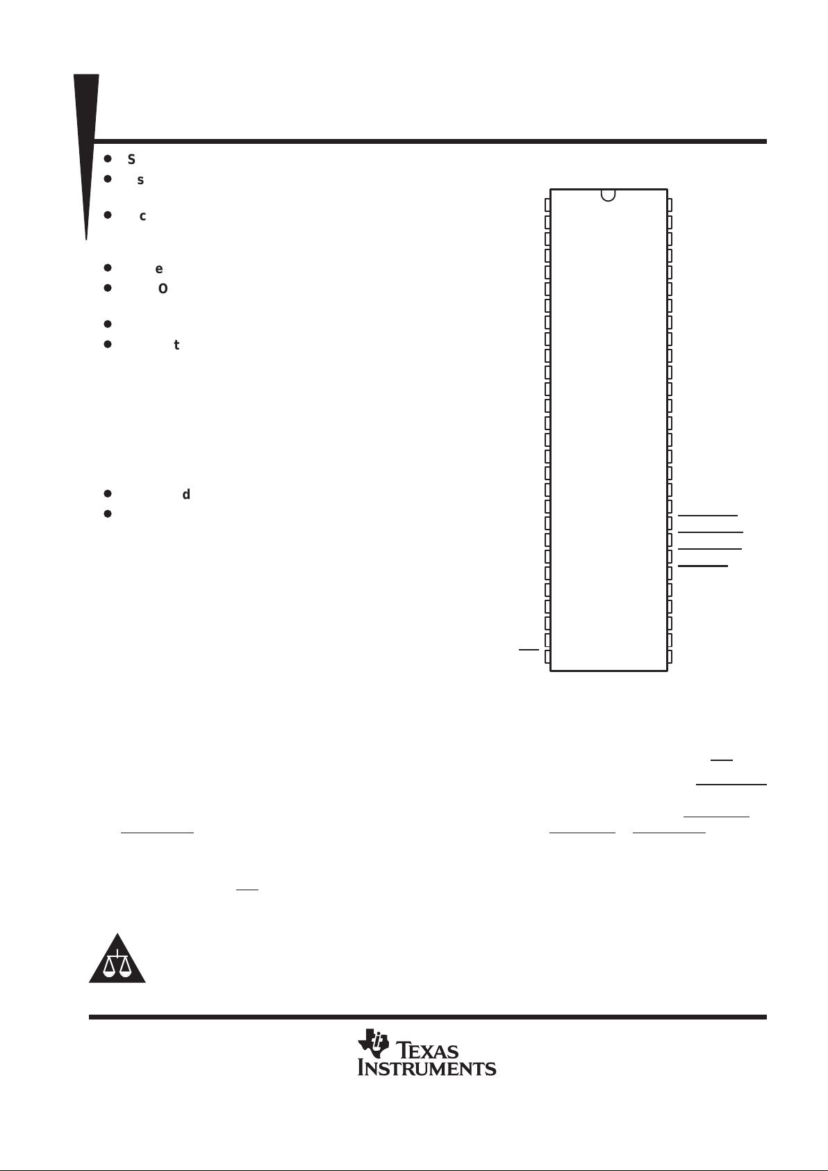
GND
REF0
REF1
V
DD
3.3V
XIN
XOUT
GND
PCI_F
PCI1
VDD3.3V
PCI2
PCI3
GND
PCI4
PCI5
VDD3.3V
PCI6
PCI7
GND
GND
3V66(0)
3V66(1)
V
DD
3.3V
GND
3V66(2)
3V66(3)
V
DD
3.3V
SEL133/100
VDD2.5V
APIC2
APIC1
APIC0
GND
V
DD
2.5V
CPU_DIV2(1)
CPU_DIV2(0)
GND
V
DD
2.5V
CPU3
CPU2
GND
V
DD
2.5V
CPU1
CPU0
GND
V
DD
3.3V
GND
PCI_STOP
CPU_STOP
PWR_DWN
SPREAD
SEL1
SEL0
V
DD
3.3V
48MHz
GND
DL PACKAGE
(TOP VIEW)
Intel and Pentium III are trademarks of Intel Corporation.
Direct Rambus and Rambus are trademarks of Rambus Inc.
Please be aware that an important notice concerning availability, standard warranty, and use in critical applications of
Texas Instruments semiconductor products and disclaimers thereto appears at the end of this data sheet.
CDC924
133-MHz CLOCK SYNTHESIZER/DRIVER FOR PC MOTHERBOARDS
WITH 3-STATE OUTPUTS
SCAS607A – NOVEMBER 1998 – REVISED MA Y 1999
2
POST OFFICE BOX 655303 • DALLAS, TEXAS 75265
description (continued)
Since the CDC924 is based on PLL circuitry, it requires a stabilization time to achieve phase lock of the PLL.
This stabilization time is required after power up or after changes to the SEL inputs are made. With use of an
external reference clock, this signal must be fixed-frequency and fixed-phase before the stabilization time starts.
function tables
SELECT FUNCTIONS
INPUTS
OUTPUTS
SEL133/
100
SEL1 SEL0 CPU CPU_DIV2 3V66
PCI,
PCI_F
48MHz REF APIC
FUNCTION
L L L Hi-Z Hi-Z Hi-Z Hi-Z Hi-Z Hi-Z Hi-Z 3-state
L L H N/A N/A N/A N/A N/A N/A N/A Reserved
L H L 100 MHz 50 MHz 66 MHz 33 MHz Hi-Z 14.318 MHz 16.67 MHz 48-MHz PLL off
L H H 100 MHz 50 MHz 66 MHz 33 MHz 48 MHz 14.318 MHz 16.67 MHz 48-MHz PLL on
H L L TCLK/2 TCLK/4 TCLK/4 TCLK/8 TCLK/2 TCLK TCLK/16 Test
H L H N/A N/A N/A N/A N/A N/A N/A Reserved
H H L 133 MHz 66 MHz 66 MHz 33 MHz Hi-Z 14.318 MHz 16.67 MHz 48-MHz PLL off
H H H 133 MHz 66 MHz 66 MHz 33 MHz 48 MHz 14.318 MHz 16.67 MHz 48-MHz PLL on
ENABLE FUNCTIONS
INPUTS
OUTPUTS INTERNAL
CPU_STOP PWR_DWN PCI_STOP CPU CPU_DIV2 APIC 3V66 PCI PCI_F
REF,
48MHz
Crystal VCOs
X L X L L L L L L L Off Off
L HLLOn On L L On On On On
L HHLOn On L On On On On On
H HLOnOn On On L On On On On
H H H On On On On On On On On On
OUTPUT BUFFER SPECIFICATIONS
BUFFER NAME
VDD RANGE
(V)
IMPEDANCE
(Ω)
BUFFER TYPE
CPU, CPU_DIV2, APIC 2.375 – 2.625 13.5 – 45 TYPE 1
48MHz, REF 3.135 – 3.465 20 – 60 TYPE 3
PCI, PCI_F, 3V66 3.135 – 3.465 12 – 55 TYPE 5
CDC924
133-MHz CLOCK SYNTHESIZER/DRIVER FOR PC MOTHERBOARDS
WITH 3-STATE OUTPUTS
SCAS607A – NOVEMBER 1998 – REVISED MA Y 1999
3
POST OFFICE BOX 655303 • DALLAS, TEXAS 75265
Terminal Functions
TERMINAL
NAME NO.
I/O
DESCRIPTION
3V66 [0–3] 21, 22, 25, 26 O 3.3 V, Type 5, 66-MHz clock outputs
48MHz 30 O 3.3 V, Type 3, 48-MHz clock output
APIC [0–2] 53, 54, 55 O 2.5 V, Type 1, APIC clock outputs
CPU [0–3] 41, 42, 45, 46 O 2.5 V, Type 1, CPU clock outputs
CPU_DIV2 [0–1] 49, 50 O 2.5 V, Type 1, CPU_DIV2 clock outputs
CPU_STOP 36 I Disables CPU clock to low state
GND 1, 7, 13, 19,
20, 24, 29, 38,
40, 44, 48, 52
Ground
PCI [1–7] 9, 11, 12, 14,
15, 17, 18
O 3.3 V, Type 5, 33-MHz PCI clock outputs
PCI_F 8 O Free-running 3.3-V, Type 5, 33-MHz PCI clock output
PCI_STOP 37 I Disables PCI clock to low state
PWR_DWN 35 I Power down for complete device with outputs forced low
REF0, REF1 2, 3 O 3.3 V, Type 3, 14.318-MHz reference clock output
SEL0, SEL1 32, 33 I L VTTL level logic select terminals for function selection
SEL133/100 28 I LVTTL level logic select pins for enabling 100/133 MHz
SPREAD 34 I Disables SSC function
VDD3.3V 4, 10, 16, 23,
27, 31, 39
Power for the 3V66, 48MHz, PCI, REF outputs and CORE logic
VDD2.5V 43, 47, 51, 56 Power for CPU and APIC outputs
XIN 5 I Crystal input – 14.318 MHz
XOUT 6 O Crystal output – 14.318 MHz
CDC924
133-MHz CLOCK SYNTHESIZER/DRIVER FOR PC MOTHERBOARDS
WITH 3-STATE OUTPUTS
SCAS607A – NOVEMBER 1998 – REVISED MA Y 1999
4
POST OFFICE BOX 655303 • DALLAS, TEXAS 75265
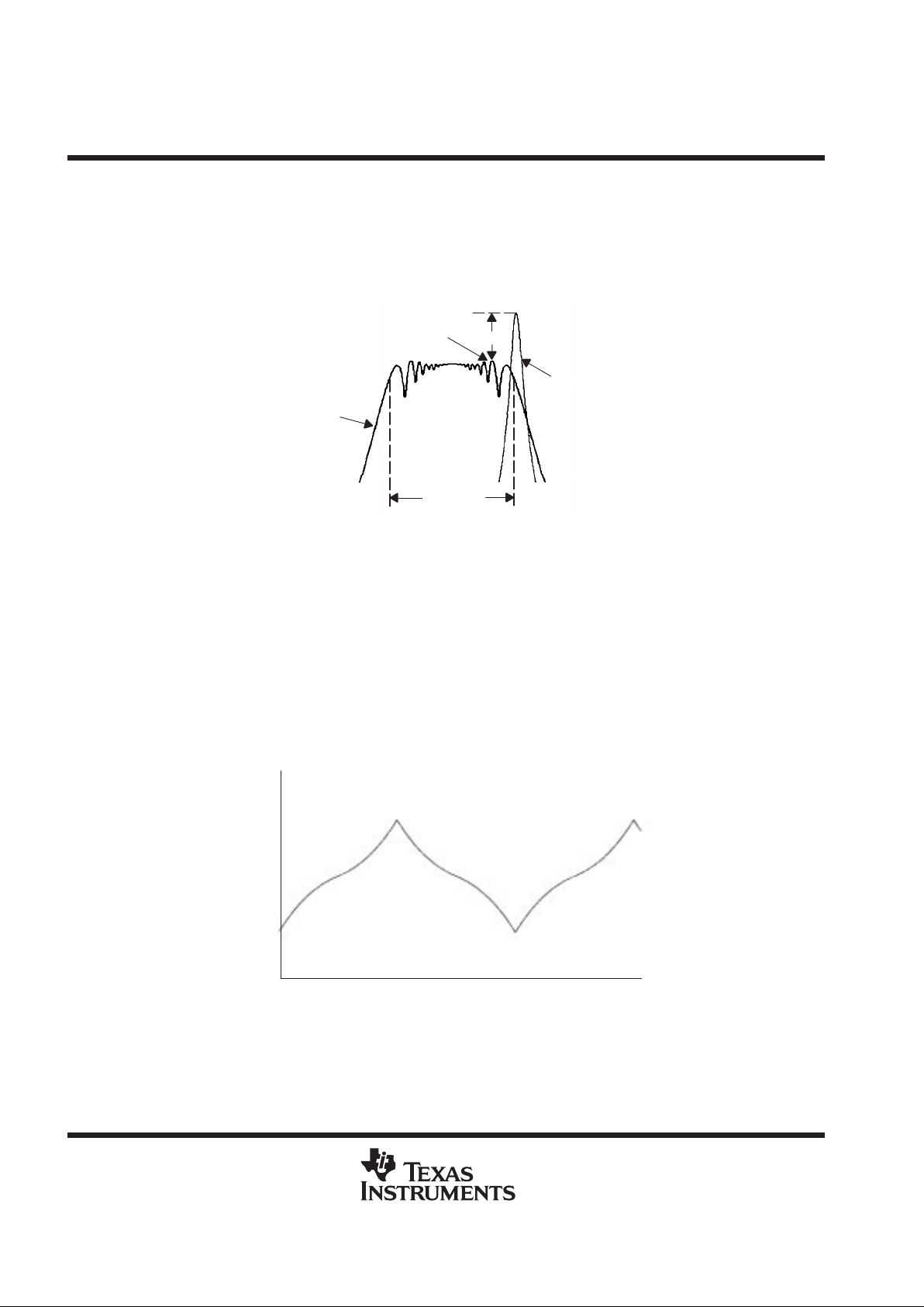
spread spectrum clock (SSC) implementation for CDC924
Simultaneously switching at fixed frequency generates a significant power peak at the selected frequency,
which in turn will cause EMI disturbance to the environment. The purpose of the internal frequency modulation
of the CPU–PLL allows to distribute the energy to many different frequencies which reduces the power peak.
A typical characteristic for a single frequency spectrum and a frequency modulated spectrum is shown in
Figure 1.
Highest Peak
Non-SSC
SSC
δ of f
nom
f
nom
∆
Figure 1. Frequency Power Spectrum With and Without the Use of SSC
The modulated spectrum has its distribution left hand to the single frequency spectrum which indicates a
“down-spread modulation”.
The peak reduction depends on the modulation scheme and modulation profile. System performance and timing
requirements are the limiting factors for actual design implementations. The implementation was driven to keep
the average clock frequency closed to its upper specification limit. The modulation amount was set to
approximately –0.5%.
In order to allow a downstream PLL to follow the frequency modulated signal, the bandwidth of the modulation
signal is limited in order to minimize SSC induced tracking skew jitter. The ideal modulation profile used for
CDC924 is shown in Figure 2.
51015202530354045
Period of Modulation Signal – µs
9.97
9.98
9.99
10
10.01
10.02
10.03
Period of Output Frequency – ns
Figure 2. SSC Modulation Profile
CDC924
133-MHz CLOCK SYNTHESIZER/DRIVER FOR PC MOTHERBOARDS
WITH 3-STATE OUTPUTS
SCAS607A – NOVEMBER 1998 – REVISED MA Y 1999
5
POST OFFICE BOX 655303 • DALLAS, TEXAS 75265
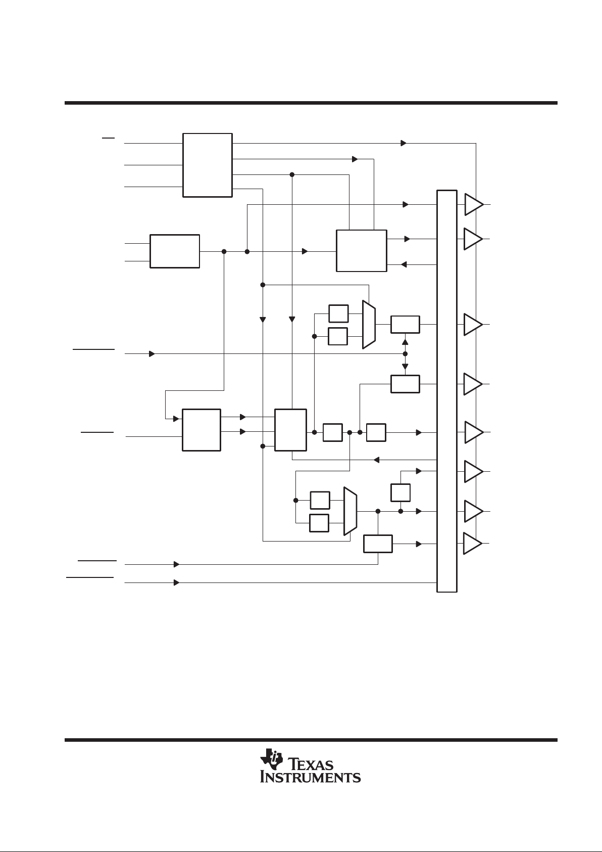
functional block diagram
2*REF
14.318 MHz
(2,3)
SEL133/100
PWR_DOWN
PCI_STOP
SPREAD
XOUT
XIN
SEL1
SEL0
Control
Logic
28
33
32
3–State
Test
48–MHz Inactive
SEL133/100
Xtal
Oscillator
6
5
48 MHz
PLL
CPU
PLL
Spread
Logic
Sync Logic & Power Down Logic
/2 /2
34
37
36
35
1*48MHz
48 MHz
(30)
3*APIC
16.67 MHz
(53, 54, 55)
1*PCI_F
33 MHz
(8)
7*PCI
33 MHz
(9,11,12,14,
15,17,18)
4*AGP (3V66)
66 MHz
(21,22,25,26)
2*CPU_DIV2
50/66 MHz
(49,50)
4*CPU
100/133 MHz
(41,42,45,46)
/3
/4
STOP
STOP
CPU_STOP
/3
/4
/2
STOP
CDC924
133-MHz CLOCK SYNTHESIZER/DRIVER FOR PC MOTHERBOARDS
WITH 3-STATE OUTPUTS
SCAS607A – NOVEMBER 1998 – REVISED MA Y 1999
6
POST OFFICE BOX 655303 • DALLAS, TEXAS 75265
absolute maximum ratings over operating free-air temperature range (unless otherwise noted)
†
Supply voltage range, V
DD
–0.5 V to 4.6 V. . . . . . . . . . . . . . . . . . . . . . . . . . . . . . . . . . . . . . . . . . . . . . . . . . . . . . . . .
Input voltage range, V
I
(see Note 1) –0.5 V to 4.6 V. . . . . . . . . . . . . . . . . . . . . . . . . . . . . . . . . . . . . . . . . . . . . . . . .
Voltage range applied to any output in the high-impedance state or power-off state,
V
O
(see Note 1) –0.5 V to VDD + 0.5 V. . . . . . . . . . . . . . . . . . . . . . . . . . . . . . . . . . . . . . . . . . . . . . . . . . . . . . . . . .
Current into any output in the low state, I
O
2 × I
OL
. . . . . . . . . . . . . . . . . . . . . . . . . . . . . . . . . . . . . . . . . . . . . . . . . .
Input clamp current, I
IK
(V
I
< 0) –18 mA. . . . . . . . . . . . . . . . . . . . . . . . . . . . . . . . . . . . . . . . . . . . . . . . . . . . . . . . . . .
Output clamp current, I
OK
(V
O
< 0) –50 mA. . . . . . . . . . . . . . . . . . . . . . . . . . . . . . . . . . . . . . . . . . . . . . . . . . . . . . . .
Operating free-air temperature range, T
A
–0°C to 85°C. . . . . . . . . . . . . . . . . . . . . . . . . . . . . . . . . . . . . . . . . . . . .
Storage temperature range, T
stg
–65°C to 150°C. . . . . . . . . . . . . . . . . . . . . . . . . . . . . . . . . . . . . . . . . . . . . . . . . . .
Lead temperature 1,6 mm (1/16 inch) from case for 10 seconds 260°C. . . . . . . . . . . . . . . . . . . . . . . . . . . . . . .
†
Stresses beyond those listed under “absolute maximum ratings” may cause permanent damage to the device. These are stress ratings only, and
functional operation of the device at these or any other conditions beyond those indicated under “recommended operating conditions” is not
implied. Exposure to absolute-maximum-rated conditions for extended periods may affect device reliability.
NOTE 1: The input and output negative-voltage ratings may be exceeded if the input and output clamp-current ratings are observed.
DISSIPATION RATING TABLE
T
≤ 25°C DERATING FACTOR
†
T
= 70°C T
= 85°C
PACKAGE
A
POWER RATNG ABOVE TA = 25°C
A
POWER RATING
A
POWER RATING
DL 1558.6 mW 12.468 mW/°C 997.5 mW 810.52 mW
†
This is the inverse of the traditional junction-to-case thermal resistance (R
θJA
) and uses a board-mounted device
at 80.2°C/W.
recommended operating conditions (see Note 2)
MIN NOM
†
MAX UNIT
pp
3.3 V 3.135 3.465
Suppl
y v
oltage, V
DD
2.5 V 2.375 2.625
V
High-level input voltage, V
IH
2
VDD +
0.3 V
V
Low-level input voltage, V
IL
GND –
0.3 V
0.8 V
Input voltage, V
I
0 V
DD
V
CPUx, CPU_DIV2x –12
p
APICx –12
High-level output current, I
OH
48MHz, REFx –14
mA
PCIx, PCI_F, 3V66x –18
CPUx, CPU_DIV2x 12
p
APICx 12
Low-level output current, I
OL
48MHz, REFx 9
mA
PCIx, PCI_F, 3V66x 12
Reference frequency, f
(XIN)
‡
Test mode 130 MHz
Crystal frequency, f
(XTAL)
§
Normal mode 13.8 14.318 14.8 MHz
Operating free-air temperature, T
A
0 85 °C
NOTE 2: Unused inputs must be held high or low to prevent them from floating.
†
All nominal values are measured at their respective nominal VDD values.
‡
Reference frequency is a test clock driven on the XIN input during the device test mode and normal mode. In test mode, XIN can be driven
externally up to f
(XIN)
= 130 MHz. If XIN is driven externally, XOUT is floating.
§
This is a series fundamental crystal with fO = 14.31818 MHz.

CDC924
133-MHz CLOCK SYNTHESIZER/DRIVER FOR PC MOTHERBOARDS
WITH 3-STATE OUTPUTS
SCAS607A – NOVEMBER 1998 – REVISED MA Y 1999
7
POST OFFICE BOX 655303 • DALLAS, TEXAS 75265
electrical characteristics over recommended operating free-air temperature range (unless
otherwise noted)
PARAMETER TEST CONDITIONS MIN TYP†MAX UNIT
V
IK
Input clamp voltage VDD = 3.135 V , II = –18 mA –1.2 V
R
I
Input resistance XIN-XOUT VDD = 3.465 V , VI = VDD –0.5 V 80 350 kΩ
XOUT VDD = 3.135 V , VI = VDD –0.5 V 20 50 mA
I
IH
High-level input current
SEL0, SEL1,
CPU_STOP
,
PCI_STOP
,
SPREAD
VDD = 3.465 V , VI = V
DD
<10 10 µA
PWR_DWN VDD = 3.465 V , VI = V
DD
<10 10 µA
SEL133/100 VDD = 3.465 V , VI = V
DD
<10 10 µA
XOUT VDD = 3.135 V , VO = 0 V –2 –5 mA
I
IL
Low-level input current
SEL0, SEL1,
CPU_STOP
,
PCI_STOP
,
SPREAD
VDD = 3.465 V , VI = GND <10 –10 µA
PWR_DWN VDD = 3.465 V , VI = GND <10 –10 µA
SEL133/100 VDD = 3.465 V , VI = GND <10 –10 µA
I
OZ
High-impedance-state output current |VDD| = max, VO = VDD or GND ±10 µA
VDD = 2.625 V ,
All outputs = low
PWR_DWN = low,
<20 100
I
Supply current
VDD = 2.625 V ,
All outputs = high
VDDx = 2.5 V,
<20 100
µA
DD
y
VDD = 3.465 V ,
All outputs = low
PWR_DWN = low,
<50 200
VDD = 3.465 V , All outputs = high 12 35 mA
p
pp
VDD = 2.625 V 1.4
I
DD(Z)
High-impedance-state supply current
VDD = 3.465 V 28
mA
pp
CL = 20 pF,
VDD = 3.465 V 114 146
Dynamic supply current
L
CPU = 133 MHz
VDD = 2.625 V 52 70
mA
C
I
Input capacitance VDD = 3.3 V, VI = VDD or GND 3.3 5.8 pF
Crystal terminal capacitance VDD = 3.3 V, VI = 0.3 V 18 18.5 22.5 pF
†
All typical values are measured at their respective nominal VDD values.

CDC924
133-MHz CLOCK SYNTHESIZER/DRIVER FOR PC MOTHERBOARDS
WITH 3-STATE OUTPUTS
SCAS607A – NOVEMBER 1998 – REVISED MA Y 1999
8
POST OFFICE BOX 655303 • DALLAS, TEXAS 75265
electrical characteristics over recommended operating free-air temperature range (unless
otherwise noted) (continued)
CPUx, CPU_DIV2x, APICx (Type 1)
PARAMETER TEST CONDITIONS MIN TYP
†
MAX UNIT
V
High-level output voltage
VDD = min to max, IOH = –1 mA
VDD –
0.1 V
V
OH
gg
VDD = 2.375 V , IOH = –12 mA 2
p
VDD = min to max, IOL = 1 mA 0.1
VOLLow-level output voltage
VDD = 2.375 V , IOL = 12 mA 0.18 0.4
V
VDD = 2.375 V , VO = 1 V –26 –42
I
OH
High-level output current
VDD = 2.5 V,
VO = 1.25 V –46
mA
VDD = 2.625 V , VO = 2.375 V –16 –27
VDD = 2.375 V , VO = 1.2 V 27 57
I
OL
Low-level output current
VDD = 2.5 V, VO = 1.25 V 63
mA
VDD = 2.625 V , VO = 0.3 V 23 43
C
O
Output capacitance VDD = 3.3 V, VO = VDD or GND 6 8.5 pF
p
p
High state VO = 0.5 VDD, VO/I
OH
13.5 27 45
ZOOutput impedance
Low state VO = 0.5 VDD, VO/I
OL
13.5 20 45
Ω
†
All typical values are measured at their respective nominal VDD values.
48MHz, REFx (Type 3)
PARAMETER TEST CONDITIONS MIN TYP
†
MAX UNIT
V
High-level output voltage
VDD = min to max, IOH = –1 mA
VDD –
0.1 V
V
OH
gg
VDD = 3.135 V , IOH = –14 mA 2.4
p
VDD = min to max, IOL = 1 mA 0.1
VOLLow-level output voltage
VDD = 3.135 V , IOL = 9 mA 0.18 0.4
V
VDD = 3.135 V , VO = 1 V –27 –41
I
OH
High-level output current
VDD = 3.3 V,
VO = 1.65 V –41
mA
VDD = 3.465 V , VO = 3.135 V –12 –23
VDD = 3.135 V , VO = 1.95 V 29 50
I
OL
Low-level output current
VDD = 3.3 V, VO = 1.65 V 53
mA
VDD = 3.465 V , VO = 0.4 V 20 37
C
O
Output capacitance VDD = 3.3 V, VO = VDD or GND 4.5 7 pF
p
p
High state VO = 0.5 VDD, VO/I
OH
20 40 60
ZOOutput impedance
Low state VO = 0.5 VDD, VO/I
OL
20 31 60
Ω
†
All typical values are measured at their respective nominal VDD values.

CDC924
133-MHz CLOCK SYNTHESIZER/DRIVER FOR PC MOTHERBOARDS
WITH 3-STATE OUTPUTS
SCAS607A – NOVEMBER 1998 – REVISED MA Y 1999
9
POST OFFICE BOX 655303 • DALLAS, TEXAS 75265
electrical characteristics over recommended operating free-air temperature range (unless
otherwise noted) (continued)
PCIx, PCI_F, 3V66x (Type 5)
PARAMETER TEST CONDITIONS MIN TYP
†
MAX UNIT
V
High-level output voltage
VDD = min to max, IOH = –1 mA
VDD –
0.1 V
V
OH
gg
VDD = 3.135 V , IOH = –18 mA 2.4
p
VDD = min to max, IOL = 1 mA 0.1
VOLLow-level output voltage
VDD = 3.135 V , IOL = 12 mA 0.15 0.4
V
VDD = 3.135 V , VO = 1 V –33 –53
I
OH
High-level output current
VDD = 3.3 V,
VO = 1.65 V –53
mA
VDD = 3.465 V , VO = 3.135 V –16 –33
VDD = 3.135 V , VO = 1.95 V 30 67
I
OL
Low-level output current
VDD = 3.3 V, VO = 1.65 V 70
mA
VDD = 3.465 V , VO = 0.4 V 27 49
C
O
Output capacitance VDD = 3.3 V, VO = VDD or GND 4.5 7.5 pF
p
p
High state VO = 0.5 VDD, VO/I
OH
12 31 55
ZOOutput impedance
Low state VO = 0.5 VDD, VO/I
OL
12 24 55
Ω
†
All typical values are measured at their respective nominal VDD values.
switching characteristics, VDD = 3.135 V to 3.465 V, TA = 0°C to 85°C
PARAMETER TEST CONDITIONS MIN TYP MAX UNIT
Overshoot/undershoot GND – 0.7 V VDD + 0.7 V V
Ring back VIL – 0.1 V VIH + 0.1 V V
Stabilization time, PWR_DWN to PCIx f
(CPU)
= 133 MHz 0.05 3 ms
t
dis3
Disable time, PWR_DWN to PCIx f
(CPU)
= 133 MHz 50 ns
Stabilization time, PWR_DWN to CPUx f
(CPU)
= 133 MHz 0.03 3 ms
t
dis4
Disable time, PWR_DWN to CPUx f
(CPU)
= 133 MHz 50 ns
After SEL1, SEL0 3
Stabilization time
†
After power up 3
ms
†
Stabilization time is the time required for the integrated PLL circuit to obtain phase lock of its feedback signal to its reference signal. In order for
phase lock to be obtained, a fixed-frequency, fixed-phase reference signal must be present at XIN. Until phase lock is obtained, the specifications
for propagation delay and skew parameters given in the switching characteristics tables are not applicable. Stabilization time is defined as the
time from when VDD achieves its nominal operating level until the output frequency is stable and operating within specification.

CDC924
133-MHz CLOCK SYNTHESIZER/DRIVER FOR PC MOTHERBOARDS
WITH 3-STATE OUTPUTS
SCAS607A – NOVEMBER 1998 – REVISED MA Y 1999
10
POST OFFICE BOX 655303 • DALLAS, TEXAS 75265
switching characteristics, VDD = 2.375 V to 2.625 V, TA = 0°C to 85°C (continued)
CPUx
PARAMETER
FROM
(INPUT)TO(OUTPUT)
TEST CONDITIONS MIN TYP MAX UNIT
t
en1
Output enable time SEL133/100 CPUx f
(CPU)
= 100 or 133MHz 6 10 ns
t
dis1
Output disable time SEL133/100 CPUx f
(CPU)
= 100 or 133MHz 8 10 ns
f
(CPU)
= 100 MHz 10 10.04 10.2 ns
t
c
CPU clock
perio
d
†
f
(CPU)
= 133 MHz 7.5 7.53 7.7 ns
Cycle to cycle jitter f
(CPU)
= 100 or 133MHz 250 ps
Duty cycle f
(CPU)
= 100 or 133MHz 45 55 %
t
sk(o)
CPU bus skew CPUx CPUx f
(CPU)
= 100 or 133MHz 50 175 ps
t
sk(p)
CPU pulse skew CPUn CPUn f
(CPU)
= 100 or 133MHz 2.2 ns
t
(off)
CPU clock to APIC clock offset, rising edge 1.5 2.8 4 ns
t
(off)
CPU clock to 3V66 clock offset, rising edge 0 0.75 1.5 ns
f
(CPU)
= 100 MHz 2.6 4.3
tw1Pulse duration width, high
f
(CPU)
= 133 MHz 1.4 3.7
ns
f
(CPU)
= 100 MHz 2.8 4.3
tw2Pulse duration width, lo
w
f
(CPU)
= 133 MHz
1.7 4
ns
t
r
Rise time VO = 0.4 V to 2.0 V 0.4 1.5 2.2 ns
t
f
Fall time VO = 0.4 V to 2.0 V 0.4 1.4 2 ns
†
The average over any 1-µs period of time is greater than the minimum specified period.
CPU_DIV2x
PARAMETER
FROM
(INPUT)TO(OUTPUT)
TEST CONDITIONS MIN TYP MAX UNIT
t
en1
Output enable time SEL133/100 CPU_DIV2x f
(CPU)
= 100 or 133MHz 6 10 ns
t
dis1
Output disable time SEL133/100 CPU_DIV2x f
(CPU)
= 100 or 133MHz 8 10 ns
p
f
(CPU)
= 100 MHz 20 20.08 20.4 ns
tcCPU_DIV2 clock period
†
f
(CPU)
= 133 MHz 15 15.06 15.3 ns
Cycle to cycle jitter f
(CPU)
= 100 or 133MHz 250 ps
Duty cycle f
(CPU)
= 100 or 133MHz 45 55 %
t
sk(o)
CPU_DIV2 bus skew CPU_DIV2x CPU_DIV2x f
(CPU)
= 100 or 133MHz 50 175 ps
t
sk(p)
CPU_DIV2 pulse skew CPU_DIV2n CPU_DIV2n f
(CPU)
= 100 or 133MHz 1.6 ns
f
(CPU)
= 100 MHz 7.1
tw1Pulse duration width, high
f
(CPU)
= 133 MHz 4.7
ns
f
(CPU)
= 100 MHz 7.3 8.9
tw2Pulse duration width, lo
w
f
(CPU)
= 133 MHz
5 6.6
ns
t
r
Rise time VO = 0.4 V to 2.0 V 0.4 1.4 2 ns
t
f
Fall time VO = 0.4 V to 2.0 V 0.4 1.3 1.8 ns
†
The average over any 1-µs period of time is greater than the minimum specified period.

CDC924
133-MHz CLOCK SYNTHESIZER/DRIVER FOR PC MOTHERBOARDS
WITH 3-STATE OUTPUTS
SCAS607A – NOVEMBER 1998 – REVISED MA Y 1999
11
POST OFFICE BOX 655303 • DALLAS, TEXAS 75265
switching characteristics, VDD = 2.375 V to 2.625 V, TA = 0°C to 85°C (continued)
APIC
PARAMETER
FROM
(INPUT)TO(OUTPUT)
TEST CONDITIONS MIN TYP MAX UNIT
t
en1
Output enable time SEL133/100 APICx f
(APIC)
= 16.67 MHz 6 10 ns
t
dis1
Output disable time SEL133/100 APICx f
(APIC)
= 16.67 MHz 8 10 ns
t
c
APIC clock period
†
f
(APIC)
= 16.67 MHz 60 60.24 60.6 ns
Cycle to cycle jitter f
(CPU)
= 100 or 133 MHz 400 ps
Duty cycle f
(APIC)
= 16.67 MHz 45 55 %
t
sk(o)
APIC bus skew APICx APICx f
(APIC)
= 16.67 MHz 30 100 ps
t
sk(p)
APIC pulse skew APICn APICn f
(APIC)
= 16.67 MHz 3 ns
t
(off)
APIC clock to CPU clock offset,
rising edge
APICx CPUx –1.5 –4 ns
t
w1
Pulse duration width, high f
(APIC)
= 16.67 MHz 25.5 28 ns
t
w2
Pulse duration width, low f
(APIC)
= 16.67 MHz 25.3 29.2 ns
t
r
Rise time VO = 0.4 V to 2 V 0.4 1.6 2.1 ns
t
f
Fall time VO = 0.4 V to 2 V 0.4 1.2 1.7 ns
†
The average over any 1-µs period of time is greater than the minimum specified period.
switching characteristics, VDD = 3.135 V to 3.465 V, TA = 0°C to 85°C
3V66
PARAMETER
FROM
(INPUT)TO(OUTPUT)
TEST CONDITIONS MIN TYP MAX UNIT
t
en1
Output enable time SEL133/100 3V66x f
(3V66)
= 66 MHz 6 10 ns
t
dis1
Output disable time SEL133/100 3V66x f
(3V66)
= 66 MHz 8 10 ns
t
c
3V66 clock period
†
f
(3V66)
= 66 MHz 15 15.06 15.3 ns
Cycle to cycle jitter f
(CPU)
= 100 or 133 MHz 400 ps
Duty cycle f
(3V66)
= 66 MHz 45 55 %
t
sk(o)
3V66 bus skew 3V66x 3V66x f
(3V66)
= 66 MHz 50 150 ps
t
sk(p)
3V66 pulse skew 3V66n 3V66n f
(3V66)
= 66 MHz 2.6 ns
t
(off)
3V66 clock to CPU clock offset 3V66x CPUx 0 –0.75 –1.5 ns
t
(off)
3V66 clock to PCI clock offset, rising edge 1.2 2.1 3 ns
t
w1
Pulse duration width, high f
(3V66)
= 66 MHz 5.2 ns
t
w2
Pulse duration width, low f
(3V66)
= 66 MHz 5 ns
t
r
Rise time VO = 0.4 V to 2 V 0.5 1.5 2 ns
t
f
Fall time VO = 0.4 V to 2 V 0.5 1.5 2 ns
†
The average over any 1-µs period of time is greater than the minimum specified period.
CDC924
133-MHz CLOCK SYNTHESIZER/DRIVER FOR PC MOTHERBOARDS
WITH 3-STATE OUTPUTS
SCAS607A – NOVEMBER 1998 – REVISED MA Y 1999
12
POST OFFICE BOX 655303 • DALLAS, TEXAS 75265
switching characteristics, VDD = 3.135 V to 3.465 V, TA = 0°C to 85°C (continued)
48MHz
PARAMETER
FROM
(INPUT)TO(OUTPUT)
TEST CONDITIONS MIN TYP MAX UNIT
t
en1
Output enable time SEL133/100 48MHz f
(48MHz)
= 48 MHz 6 10 ns
t
dis1
Output disable time SEL133/100 48MHz f
(48MHz)
= 48 MHz 8 10 ns
t
c
48MHz clock period
†
f
(48MHz)
= 48 MHz 20.5 20.83 21.1 ns
Cycle to cycle jitter f
(CPU)
= 100 or 133 MHz 500 ps
Duty cycle f
(48MHz)
= 48 MHz 45 55 %
t
sk(p)
48MHz pulse skew 48MHz 48MHz f
(48MHz)
= 48 MHz 3 ns
t
w1
Pulse duration width, high f
(48MHz)
= 48 MHz 7.8 ns
t
w2
Pulse duration width, low f
(48MHz)
= 48 MHz 7.8 ns
t
r
Rise time VO = 0.4 V to 2 V 1 2.1 2.8 ns
t
f
Fall time VO = 0.4 V to 2 V 1 1.9 2.8 ns
†
The average over any 1-µs period of time is greater than the minimum specified period.
REF
PARAMETER
FROM
(INPUT)TO(OUTPUT)
TEST CONDITIONS MIN TYP MAX UNIT
t
en1
Output enable time SEL133/100 REFx f
(REF)
= 14.318 MHz 6 10 ns
t
dis1
Output disable time SEL133/100 REFx f
(REF)
= 14.318 MHz 8 10 ns
t
c
REF clock period
†
f
(REF)
= 14.318 MHz 69.84 ns
Cycle to cycle jitter f
(CPU)
= 100 or 133 MHz 700 ps
Duty cycle f
(REF)
= 14.318 MHz 45 55 %
t
sk(o)
REF bus skew REFx REFx f
(REF)
= 14.318 MHz 150 250 ps
t
sk(p)
REF pulse skew REFn REFn f
(REF)
= 14.318 MHz 2 ns
t
w1
Pulse duration width, high f
(REF)
= 14.318 MHz 26.2 32.7 ns
t
w2
Pulse duration width, low f
(REF)
= 14.318 MHz 26.2 31.2 ns
t
r
Rise time VO = 0.4 V to 2 V 1 2 2.8 ns
t
f
Fall time VO = 0.4 V to 2 V 1 1.9 2.8 ns
†
The average over any 1-µs period of time is greater than the minimum specified period.

CDC924
133-MHz CLOCK SYNTHESIZER/DRIVER FOR PC MOTHERBOARDS
WITH 3-STATE OUTPUTS
SCAS607A – NOVEMBER 1998 – REVISED MA Y 1999
13
POST OFFICE BOX 655303 • DALLAS, TEXAS 75265
switching characteristics, VDD = 3.135 V to 3.465 V, TA = 0°C to 85°C (continued)
PCI, PCI_F
PARAMETER
FROM
(INPUT)TO(OUTPUT)
TEST CONDITIONS MIN TYP MAX UNIT
t
en1
Output enable time SEL133/100 PCIx f
(PCI)
= 33 MHz 6 10 ns
t
dis1
Output disable time SEL133/100 PCIx f
(PCI)
= 33 MHz 8 10 ns
t
c
PCIx clock period
†
f
(PCI)
= 33 MHz 30 30.12 30.5 ns
Cycle to cycle jitter f
(CPU)
= 100 or 133 MHz 300 ps
Duty cycle f
(PCI)
= 33 MHz 45 55 %
t
sk(o)
PCIx bus skew PCIx PCIx f
(PCI)
= 33 MHz 70 300 ps
t
sk(p)
PCIx pulse skew PCIn PCIn f
(PCI)
= 33 MHz 4 ns
t
(off)
PCIx clock to 3V66 clock offset –1.2 –3 ns
t
w1
Pulse duration width, high f
(PCI)
= 33 MHz 12 ns
t
w2
Pulse duration width, low f
(PCI)
= 33 MHz 12 ns
t
r
Rise time VO = 0.4 V to 2 V 0.5 1.6 2 ns
t
f
Fall time VO = 0.4 V to 2 V 0.5 1.5 2 ns
†
The average over any 1-µs period of time is greater than the minimum specified period.

CDC924
133-MHz CLOCK SYNTHESIZER/DRIVER FOR PC MOTHERBOARDS
WITH 3-STATE OUTPUTS
SCAS607A – NOVEMBER 1998 – REVISED MA Y 1999
14
POST OFFICE BOX 655303 • DALLAS, TEXAS 75265
PARAMETER MEASUREMENT INFORMATION
RL = 500 Ω
LOAD CIRCUIT for tpd and t
sk
From Output
Under Test
C
L
(see Note A)
RL = 500 Ω
S1
V
O_REF
OPEN
GND
t
PLH/tPHL
t
PLZ/tPZL
t
PHZ/tPZH
Open
V
O_REF
GND
TEST S1
t
w
Input
3 V
0 V
V
IH_REF
V
T_REF
V
IL_REF
From Output
Under Test
Test
Point
C
L
(see Note A)
LOAD CIRCUIT FOR tr and t
f
VOLTAGE WAVEFORMS
0 V
Output
Waveform 2
S1 at GND
(see Note B)
VOLTAGE WAVEFORMS
V
OH
V
OL
V
DD
V
T_REF
V
T_REF
V
T_REF
t
PZL
t
PLZ
t
PHZ
t
PZH
V
T_REF
VOH – 0.3 V
VOL + 0.3 V
≈3 V
≈0 V
Output
Waveform 1
S1 at 6 V
(see Note B)
Output
Enable
(high-level
enabling)
t
r
3 V
0 V
V
IH_REF
V
T_REF
V
IL_REF
V
T_REF
V
T_REF
t
PLH
t
PHL
t
f
t
w_high
t
w_low
V
OH
V
OL
Input
Output
VOLTAGE WAVEFORMS
NOTES: A. CL includes probe and jig capacitance. CL = 20 pF (CPUx, APICx, 48MHz, REF), CL = 30 pF (PCIx, 3V66)
B. Waveform 1 is for an output with internal conditions such that the output is low except when disabled by the output control.
Waveform 2 is for an output with internal conditions such that the output is high except when disabled by the output control.
C. All input pulses are supplied by generators having the following characteristics: PRR v 14.318 MHz, ZO = 50 Ω, tr ≤ 2.5 ns,
tf ≤ 2.5 ns.
D. The outputs are measured one at a time with one transition per measurement.
PARAMETER
3.3-V INTERFACE 2.5-V INTERFACE UNIT
V
IH_REF
High-level reference voltage 2.4 2 V
V
IL_REF
Low-level reference voltage 0.4 0.4 V
V
T_REF
Input Threshold reference voltage 1.5 1.25 V
V
O_REF
Off-state reference voltage 6 4.6 V
Figure 3. Load Circuit and Voltage Waveforms

CDC924
133-MHz CLOCK SYNTHESIZER/DRIVER FOR PC MOTHERBOARDS
WITH 3-STATE OUTPUTS
SCAS607A – NOVEMBER 1998 – REVISED MA Y 1999
15
POST OFFICE BOX 655303 • DALLAS, TEXAS 75265
PARAMETER MEASUREMENT INFORMATION
t
sk(o)
V
T_REF
CPUx or PCIx Clock
3V66 or CPUx
CPUx or PCIx Clock
VT_REF
V
T_REF
t
(low)
t
(high)
t
c
t
sk(p)
+Ťt
PLH–tPHL
Ť
Duty Cycle
+
t
(low or high)
t
c
100
VT_REF
t
(off)
[3V66 to PCIx]
t
(off)
[CPUx to APICx]
t
(off)
[CPUx to 3V66]
3V66, PCIx, or APICx
Figure 4. Waveforms for Calculation of Skew, Offset, and Jitter
CPU
(internal)
PCI
(internal)
CPU_STOP
PCI_STOP
PWR_DOWN
PCI_F
(external)
CPU
(external)
3V66
(external)
Figure 5. CPU_STOP Timing

CDC924
133-MHz CLOCK SYNTHESIZER/DRIVER FOR PC MOTHERBOARDS
WITH 3-STATE OUTPUTS
SCAS607A – NOVEMBER 1998 – REVISED MA Y 1999
16
POST OFFICE BOX 655303 • DALLAS, TEXAS 75265
PARAMETER MEASUREMENT INFORMATION
CPU
(internal)
PCI
(internal)
CPU_STOP
PCI_STOP
PWR_DOWN
PCI_F
(external)
PCI
(external)
Figure 6. PCI_STOP Timing
CPU
(internal)
PCI
(internal)
PWR_DOWN
PCI
(external)
CPU
(external)
VCO
CRYSTAL
NOTE A: Shaded sections on the VCO and Crystal waveforms indicate that the VCO and crystal oscillators are active and there is a valid clock.
Figure 7. Power-Down Timing

CDC924
133-MHz CLOCK SYNTHESIZER/DRIVER FOR PC MOTHERBOARDS
WITH 3-STATE OUTPUTS
SCAS607A – NOVEMBER 1998 – REVISED MA Y 1999
17
POST OFFICE BOX 655303 • DALLAS, TEXAS 75265
MECHANICAL DATA
DL (R-PDSO-G**) PLASTIC SMALL-OUTLINE PACKAGE
4040048/D 08/97
48-PIN SHOWN
56
0.730
(18,54)
0.720
(18,29)
4828
0.370
(9,40)
(9,65)
0.380
Gage Plane
DIM
0.420 (10,67)
0.395 (10,03)
A MIN
A MAX
0.006 (0,15) NOM
PINS **
0.630
(16,00)
(15,75)
0.620
0.010 (0,25)
Seating Plane
0.020 (0,51)
0.040 (1,02)
25
24
0.008 (0,203)
0.012 (0,305)
48
1
0.008 (0,20) MIN
A
0.110 (2,79) MAX
0.299 (7,59)
0.291 (7,39)
0.004 (0,10)
M
0.005 (0,13)
0.025 (0,635)
0°–8°
NOTES: B. All linear dimensions are in inches (millimeters).
C. This drawing is subject to change without notice.
D. Body dimensions do not include mold flash or protrusion not to exceed 0.006 (0,15).
E. Falls within JEDEC MO-118

IMPORTANT NOTICE
T exas Instruments and its subsidiaries (TI) reserve the right to make changes to their products or to discontinue
any product or service without notice, and advise customers to obtain the latest version of relevant information
to verify, before placing orders, that information being relied on is current and complete. All products are sold
subject to the terms and conditions of sale supplied at the time of order acknowledgement, including those
pertaining to warranty, patent infringement, and limitation of liability.
TI warrants performance of its semiconductor products to the specifications applicable at the time of sale in
accordance with TI’s standard warranty. Testing and other quality control techniques are utilized to the extent
TI deems necessary to support this warranty. Specific testing of all parameters of each device is not necessarily
performed, except those mandated by government requirements.
CERT AIN APPLICATIONS USING SEMICONDUCTOR PRODUCTS MAY INVOLVE POTENTIAL RISKS OF
DEATH, PERSONAL INJURY, OR SEVERE PROPERTY OR ENVIRONMENTAL DAMAGE (“CRITICAL
APPLICATIONS”). TI SEMICONDUCTOR PRODUCTS ARE NOT DESIGNED, AUTHORIZED, OR
WARRANTED TO BE SUITABLE FOR USE IN LIFE-SUPPORT DEVICES OR SYSTEMS OR OTHER
CRITICAL APPLICATIONS. INCLUSION OF TI PRODUCTS IN SUCH APPLICA TIONS IS UNDERST OOD TO
BE FULLY AT THE CUSTOMER’S RISK.
In order to minimize risks associated with the customer’s applications, adequate design and operating
safeguards must be provided by the customer to minimize inherent or procedural hazards.
TI assumes no liability for applications assistance or customer product design. TI does not warrant or represent
that any license, either express or implied, is granted under any patent right, copyright, mask work right, or other
intellectual property right of TI covering or relating to any combination, machine, or process in which such
semiconductor products or services might be or are used. TI’s publication of information regarding any third
party’s products or services does not constitute TI’s approval, warranty or endorsement thereof.
Copyright 1999, Texas Instruments Incorporated
 Loading...