

Page 1
查询CDC857供应商
CDC857-2, CDC857-3
2.5-/3.3-V PHASE-LOCK LOOP CLOCK DRIVERS
SCAS627A – SEPTEMBER 1999 – DECEMBER 1999
D
Phase-Lock Loop Clock Distribution for
Double Data Rate Synchronous DRAM
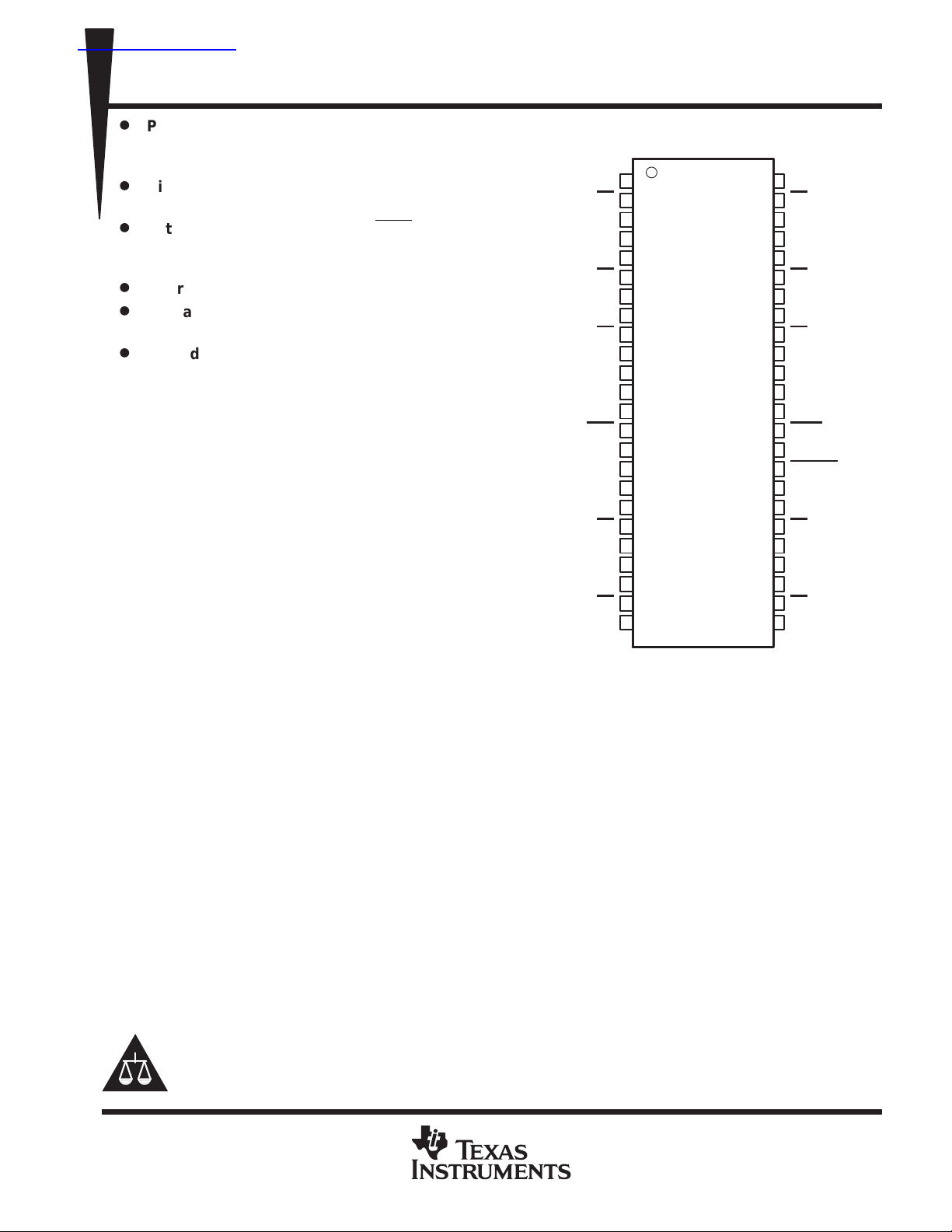
DGG PACKAGE
(TOP VIEW)
Applications
D
Distributes One Differential Clock Input to
Ten Differential Outputs
D
External Feedback Pins (FBIN, FBIN) Are
Used to Synchronize the Outputs to the
Clock Input
D
Operates at VCC = 2.5 V and AVCC = 3.3 V
D
Packaged in Plastic 48-Pin (DGG) Thin
Shrink Small-Outline Package (TSSOP)
D
Spread Spectrum Clocking Tracking
Capability to Reduce EMI
description
The CDC857-2 and CDC857-3 are high-performance, low-skew, low-jitter, phase-lock loop
(PLL) clock driver. They use a PLL to precisely
align, in both frequency and phase, the feedback
(FBOUT) output to the clock (CLK) input signal.
The CDC857-3 operates at 3.3 V (PLL) and 2.5 V
(output buffer). The CDC857-2 operates at
2.5 V (PLL and output buffer).
One bank of ten inverting and noninverting
outputs provide ten low-skew, low-jitter copies of
GND
Y0
Y0
V
CC
Y1
Y1
GND
GND
Y2
Y2
V
CC
V
CC
CLK
CLK
V
CC
AV
CC
AGND
GND
Y3
Y3
V
CC
Y4
Y4
GND
1
2
3
4
5
6
7
8
9
10
11
12
13
14
15
16
17
18
19
20
21
22
23
24
48
47
46
45
44
43
42
41
40
39
38
37
36
35
34
33
32
31
30
29
28
27
26
25
GND
Y5
Y5
V
Y6
Y6
GND
GND
Y7
Y7
V
G
FBIN
FBIN
V
FBOUT
FBOUT
GND
Y8
Y8
V
Y9
Y9
GND
CLK. Output signal duty cycles are adjusted to
50%, independent of the duty cycle at CLK.
All outputs can be enabled or disabled via a single output enable input. When the G input is high, the outputs
switch in phase and frequency with CLK; when the G input is low, the outputs are disabled to high impedance
state (3-state).
CC
CC
CC
CC
Unlike many products containing PLLs, the CDC857 does not require external RC networks. The loop filter for
the PLL is included on-chip, minimizing component count, board space, and cost.
Because it is based on PLL circuity, the CDC857 requires a stabilization time to achieve phase lock of the
feedback signal to the reference signal. This stabilization time is required following power up and application
of a fixed-frequency, fixed-phase signal at CLK, as well as following any changes to the PLL reference or
feedback signals. The PLL can be bypassed for test purposes by strapping A V
to ground. If A VCC is at GND
CC
and VCC = ON, 2 falling edges on G cause the PLL to run with FBOUT being enabled and all other outputs being
disabled, after A VCC ramps up to its specified VCC value, with G being kept low. The CDC857 is characterized
for operation from 0°C to 85°C.
Please be aware that an important notice concerning availability, standard warranty, and use in critical applications of
Texas Instruments semiconductor products and disclaimers thereto appears at the end of this data sheet.
PRODUCTION DATA information is current as of publication date.
Products conform to specifications per the terms of Texas Instruments
standard warranty. Production processing does not necessarily include
testing of all parameters.
POST OFFICE BOX 655303 • DALLAS, TEXAS 75265
Copyright 1999, Texas Instruments Incorporated
1
Page 2
CDC857-2, CDC857-3
PLL
2.5-/3.3-V PHASE-LOCK LOOP CLOCK DRIVERS
SCAS627A – SEPTEMBER 1999 – DECEMBER 1999
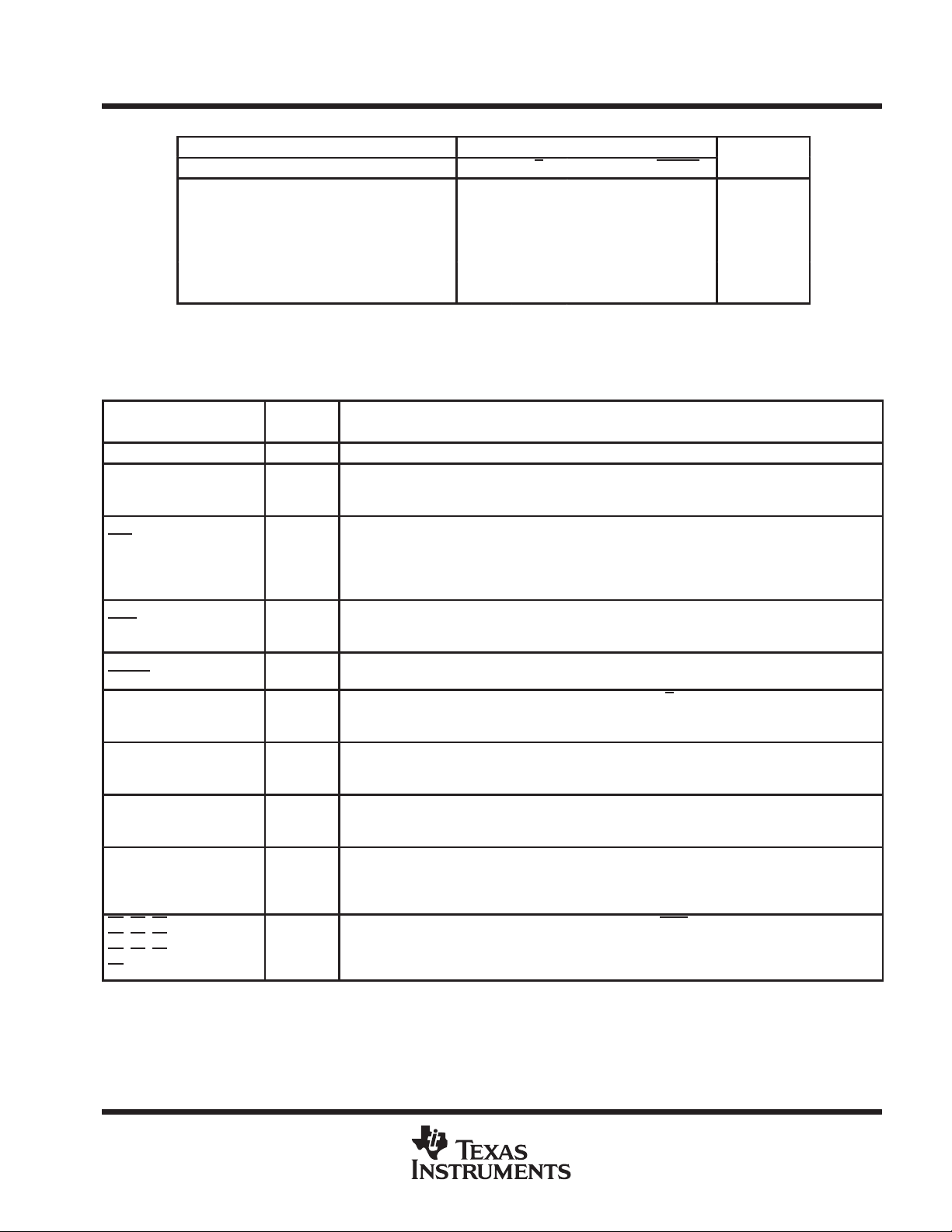
FUNCTION TABLE
INPUTS
G CLK CLK Y Y FBOUT FBOUT
L X X Z Z Z Z OFF
H LHLH L H RUN
H HLHL H L RUN
H < 20 MHz < 20 MHz Z Z Z Z OFF
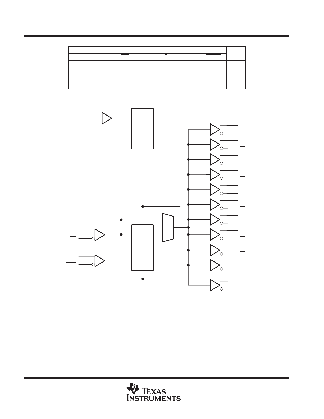
logic symbol
OUTPUTS
Clk
Clk
FBIN
FBIN
G
AV
CC
Test
Mode
Logic
PLL
Y0
Y0
Y1
Y1
Y2
Y2
Y3
Y3
Y4
Y4
Y5
Y5
Y6
Y6
Y7
Y7
Y8
Y8
Y9
Y9
AVCC = 3.3 V
NOTE A: All outputs are connected to VCC = 2.5 V.
2
POST OFFICE BOX 655303 • DALLAS, TEXAS 75265
FBOUT
FBOUT
Page 3
COMMENTS
I/O
DESCRIPTION
CDC857-2, CDC857-3
2.5-/3.3-V PHASE-LOCK LOOP CLOCK DRIVERS
SCAS627A – SEPTEMBER 1999 – DECEMBER 1999
SPECIAL TEST MODES
INPUTS
V
CC
ON 0 V L L Z Z Z Z Clock Mode
ON 0 V L H Z Z Z Z Clock Mode
ON 0 V H L L H L H Clock Mode
ON 0 V H H H L H L Clock Mode
ON UP
ON UP
†
Only one signal shown for this differential input.
‡
AVCC ramped up after two (2) high-to-low transitions on G input & G being low.
§
At least two (2) high-to-low transitions during AVCC = 0.
AV
CC
G CLK
‡
‡
§
↓
§
↓
†
LZZ L H PLL Mode
H Z Z H L PLL Mode
Y Y FBOUT FBOUT
Terminal Functions
TERMINAL
NAME NO.
AGND 17 Ground Analog ground. AGND provides the ground reference for the analog circuitry .
AV
CC
CLK
CLK
FBIN
FBIN
FBOUT
FBOUT
G 37 I Output bank enable. G is the output enable for outputs Y and Y . When G is low outputs Y are disabled
GND 1, 7, 8, 18,
V
CC
Y0, Y1, Y2,
Y3, Y4, Y5,
Y6, Y7, Y8,
Y9
Y0, Y1, Y2,
Y3
, Y4, Y5,
, Y7, Y8,
Y6
Y9
16 Power Analog power supply . AVCC provides the power reference for the analog circuitry. In addition, AV
13
14
36
35
32
33
24, 25, 31,
41, 42, 48
4, 11, 12,
15, 21, 28,
34, 38, 45
3, 5, 10,
20, 22, 46,
44, 39, 29,
27
2, 6, 9,
19, 23, 47,
43, 40, 30,
26
O Feedback output. FBOUT is dedicated for external feedback. It switches at the same frequency as
Ground Ground
Power Power supply
O Clock outputs. These outputs provide low-skew copies of CLK.
O Clock outputs. These outputs provide low-skew copies of CLK.
can be used to bypass the PLL for test purposes. When AVCC is strapped to ground, PLL is bypassed
and CLK is buffered directly to the device outputs. During disable (G = 0), the PLL is powered down.
I Clock input, CLK provides the clock signal to be distributed by the CDC857 clock driver. CLK is used
to provide the reference signal to the integrated PLL that generates the clock output signals. CLK
must have a fixed frequency and fixed phase for the PLL to obtain phase lock. Once the circuit is
powered up and a valid CLK signal is applied, a stabilization time is required for the PLL to phase
lock the feedback signal to its reference signal.
I Feedback input. FBIN provides the feedback signal to the internal PLL. FBIN must be hard-wired
to FBOUT to complete the PLL. The integrated PLL synchronizes CLK and FBIN so that there is
nominally zero phase error between CLK and FBIN.
CLK. When externally wired to FBIN, FBOUT completes the feedback loop of the PLL.
to a high-impedance state. When G is high, all outputs Y are enabled and switch at the same
frequency as CLK.
OUTPUTS
CC
POST OFFICE BOX 655303 • DALLAS, TEXAS 75265
3
Page 4
CDC857-2, CDC857-3
Analog suppl
oltage, AV
gg,
ID
2.5-/3.3-V PHASE-LOCK LOOP CLOCK DRIVERS
SCAS627A – SEPTEMBER 1999 – DECEMBER 1999
absolute maximum ratings over operating free-air temperature (unless otherwise noted)
†
Supply voltage range, VCC or AVCC –0.5 V to 4.6 V. . . . . . . . . . . . . . . . . . . . . . . . . . . . . . . . . . . . . . . . . . . . . . . . .
Input voltage range VI (see Notes 1 and 2) –0.5 V to VCC +0.5 V. . . . . . . . . . . . . . . . . . . . . . . . . . . . . . . . . . . . .
Output voltage range, VO, (see Notes 1 and 2) –0.5 V to VCC +0.5 V. . . . . . . . . . . . . . . . . . . . . . . . . . . . . . . . .
Input clamp current, I
(VI < 0 or VI > VCC) ±50 mA. . . . . . . . . . . . . . . . . . . . . . . . . . . . . . . . . . . . . . . . . . . . . . . .
IK
Output clamp current, IOK (VO < 0 or VO > VCC ±50 mA. . . . . . . . . . . . . . . . . . . . . . . . . . . . . . . . . . . . . . . . . . . .
Continuous total output current, IO (VO = 0 to VCC) ±50 mA. . . . . . . . . . . . . . . . . . . . . . . . . . . . . . . . . . . . . . . . .
Package thermal impedance, θJA (see Note 3) 89°C/W. . . . . . . . . . . . . . . . . . . . . . . . . . . . . . . . . . . . . . . . . . . . .
Storage temperature range T
†
Stresses beyond those listed under “absolute maximum ratings” may cause permanent damage to the device. These are stress ratings only, and
functional operation of the device at these or any other conditions beyond those indicated under “recommended operating conditions” is not
implied. Exposure to absolute-maximum-rated conditions for extended periods may affect device reliability.
NOTES: 1. The input and output negative voltage ratings may be exceeded if the input and output clamp-current ratings are observed.
2. This value is limited to 4.6 V maximum.
3. The package thermal impedance is calculated in accordance with JESD 51.
–65°C to 150°C. . . . . . . . . . . . . . . . . . . . . . . . . . . . . . . . . . . . . . . . . . . . . . . . . . . .
stg
recommended operating conditions (see Note 4)
MIN NOM MAX UNIT
Supply voltage, V
Low–level input voltage, VIL(G)
High–level input voltage, VIH(G)
DC input signal voltage (see Note 5) CLK, FBIN –0.3 VCC+0.3 V
Differential input signal voltage, V
(see Note 6)
Differential cross-point input voltage (see Note 7) VCC/2–0.2 VCC/2 VCC/2+0.2 V
High-level output current, I
Low-level output current, I
Input slew rate, SR 1 V/ns
Operating free-air temperature, T
NOTES: 4. Unused inputs must be held high or low to prevent them from floating.
CC
pp
y v
5. DC input signal voltage specifies the allowable dc execution of differential input.
6. Differential input signal voltage specifies the differential voltage |VTR – VCP| required for switching, where VTR is the true input level
and VCP is the complementary input level (see figure 3).
7. Differential cross-point voltage is expected to track variations of VCC and is the voltage at which the differential signals must be
crossing.
CC
OH
OL
A
CDC857–2 2.3 2.7 V
CDC857–3 3 3.6 V
G input 0.3 × V
G input 0.7 × V
dc CLK, FBIN 0.35 VCC+0.6 V
ac CLK, FBIN 0.7 VCC+0.6 V
2.3 2.7 V
CC
CC
–12 mA
12 mA
0 85 °C
V
V
4
POST OFFICE BOX 655303 • DALLAS, TEXAS 75265
Page 5

VOHHigh-level output voltage
V
VOLLow-level output voltage
V
IIInput current
A
IOZHigh-impedance output current
V
2.7 V
V
V
or GND
±10
A
AI
Su ly current on
mA
CDC857-2, CDC857-3
2.5-/3.3-V PHASE-LOCK LOOP CLOCK DRIVERS
SCAS627A – SEPTEMBER 1999 – DECEMBER 1999
electrical characteristics over recommended operating free-air temperature range (unless
otherwise noted)
PARAMETER TEST CONDITIONS MIN TYP
V
IK
I
OH
I
OL
V
O
V
OC
I
CCZ
l
CC
CC
C
I
C
O
†
All typical values are at respective nominal VCC.
‡
The value of VOC is expected to be |VTR + VCP|/2. In case of each clock directly terminated by a 120-Ω resistor, where VTR is the true input
signal voltage and VCP is the complementary input signal voltage (see Figure 3).
Input voltage All input pins VCC = 2.3 V, II = –18 mA –1.2 V
p
p
High-level output current VCC = 2.3 V, VO = 1 V –18 –32 mA
Low-level output current VCC = 2.3 V, VO = 1.2 V 26 35 mA
Output voltage swing For load condition see Figure 3 1.1 VCC–0.4 V
p
p
Output crossing point voltage
Supply current, disabled
Supply current on V
(see Figure 7)
Supply current on
AV
CC
Input capacitance VCC = 2.5 V, VI = VCC or GND 2 pF
Output capacitance VCC = 2.5 V,VO = VCC or GND 3 pF
G
CLK, FBIN VCC = 2.7 V, VI = 0 V to 2.7 V ±10
p
‡
CC
CDC857–2 AVCC = 2.7 V, fO = 167 MHz 9 12
CDC857–3
VCC = min to max, I
VCC = 2.3 V, IOH = –12 mA 1.7
VCC = min to max, IOL = 1 mA 0.1
VCC = 2.3 V, IOL = 12 mA 0.6
VCC = 2.7 V, VI = 0 V to 2.7 V ±10
=
CC
AVCC and VCC = max,
G = L or no input CLK signal
VCC = 2.7 V, fO = 167 MHz,
All outputs switching 16 pF in 60 Ω
environment, See Figure 3
AVCC = 3.6 V, fO = 167 MHz 15 19
,
–1 mA VCC–0.1
OH=
=
CC
O
(VCC/2)–
0.1
†
MAX UNIT
VCC/2
(VCC/2)+
0.1
500 800 µA
235 300 mA
µ
µ
V
POST OFFICE BOX 655303 • DALLAS, TEXAS 75265
5
Page 6

CDC857-2, CDC857-3
t
Jitter (peak-to–peak)
ps
t
Jitter (cycle-to-cycle)
ps
All differential in ut and out ut termi
Duty cycle
§
(see Figure 6)
2.5-/3.3-V PHASE-LOCK LOOP CLOCK DRIVERS
SCAS627A – SEPTEMBER 1999 – DECEMBER 1999
timing requirements over recommended ranges or supply voltage and operating free–air
temperature
PARAMETER TEST CONDITIONS MIN MAX UNIT
f
Clock frequency 66 167 MHz
C
Input clock duty cycle 40% 60%
Stabilization time
†
Time required for the integrated PLL circuit to obtain phase lock of its feedback signal to its reference signal. For phase lock to be obtained, a
fixed–frequency, fixed–phase reference signal must be present at CLK. Until phase lock is obtained, the specifications for propagation delay,
skew, and jitter parameters given in the switching characteristics table are not applicable. This parameter does not apply for input modulation
under SSC application.
switching characteristics
‡
t
PLH
‡
t
PHL
t
en
t
dis
(jitter)
(jitter)
t
(phase error)
t
skew(0)
t
skew(p)
tr, t
f
‡
Refers to transition of noninverting output.
§
While the pulse skew is almost constant over frequency, the duty cycle error increases at higher frequencies. This is due to the formula: duty
cycle = twH/tc, were the cycle time (tc) decreases as the frequency goes up.
Low–to high level propagation delay time
(see Figure 5)
High–to low level propagation delay time
(see Figure 5)
Output enable time CLK mode/G to any Y output 3 ns
Output disable time CLK mode/G to any Y output 3 ns
Phase error (see Figure 4)
Output skew (see Figure 4)
Pulse skew
Output rise and fall times (20% – 80%) Load = 120 Ω/16 pF 650 800 950 ps
†
PARAMETER TEST CONDITIONS MIN NOM MAX UNIT
CLK mode/CLK to any output 1.5 3.5 6 ns
CLK mode/CLK to any output 1.5 3.5 6 ns
p
p
66 MHz 120
100/125/133/167 MHz 75
66 MHz 110
100/125/133/167 MHz 65
nals are terminated with 120 Ω/
16 pF as shown in Figure 2
66 MHz to 100 MHz 49.5% 50.5%
101 MHz to 167 MHz 49% 51%
p
p
–150 150 ps
-
0.1 ms
p
p
100 ps
100 ps
6
POST OFFICE BOX 655303 • DALLAS, TEXAS 75265
Page 7

STRUCTURE
CDC857-2, CDC857-3
2.5-/3.3-V PHASE-LOCK LOOP CLOCK DRIVERS
SCAS627A – SEPTEMBER 1999 – DECEMBER 1999
APPLICATION EXAMPLE
Table 1. Clock Structure and SDRAM Loads per Clock
CLK
CLK
CLOCK
1 2 5 8
2 4 10 16
SDRAM represents
a capacitive load
120 Ω16 pF
120 Ω16 pF
NUMBER of
SDRAM LOADS
PER CLOCK
PLL
FBIN
FBIN
CAPACITIVE LOADING ON
THE PLL OUTPUTS (pF)
MIN MAX
≈ 2.5” ≈ 0.6” (Split to Terminator)
SDRAM
VTR
120 Ω
VCP
SDRAM
0.3”
Figure 1. Clock Structure #1
POST OFFICE BOX 655303 • DALLAS, TEXAS 75265
7
Page 8

CDC857-2, CDC857-3
2.5-/3.3-V PHASE-LOCK LOOP CLOCK DRIVERS
SCAS627A – SEPTEMBER 1999 – DECEMBER 1999
APPLICATION EXAMPLE
≈ 2.5” ≈ 0.6” (Split to Terminator)
SDRAM represents
a capacitive load
CLK
120 Ω16 pF
CLK
120 Ω16 pF
PLL
FBIN
FBIN
0.3”
Figure 2. Clock Structure #2
differential clock signals
Figure 3 shows the differential clocks are directly terminated by a 120-Ω resistor.
SDRAM
Stack
VTR
120 Ω
VCP
SDRAM
Stack
Device
Under
Test
V
CC
OUT
OUT
V
CC
60 Ω
60 Ω
VTR
RT = 120 Ω
VCP
Figure 3. Differential Signal Using Direct Termination Resistor
Receiver
8
POST OFFICE BOX 655303 • DALLAS, TEXAS 75265
Page 9

CDC857-2, CDC857-3
2.5-/3.3-V PHASE-LOCK LOOP CLOCK DRIVERS
SCAS627A – SEPTEMBER 1999 – DECEMBER 1999
PARAMETER MEASUREMENT INFORMATION
CLKIN
FBIN
t
(phase error)
FBOUT
Yx
t
sk(o)
Yx
Yx
t
sk(o)
Figure 4. Phase Error and Skew Waveforms
POST OFFICE BOX 655303 • DALLAS, TEXAS 75265
9
Page 10

CDC857-2, CDC857-3
2.5-/3.3-V PHASE-LOCK LOOP CLOCK DRIVERS
SCAS627A – SEPTEMBER 1999 – DECEMBER 1999
PARAMETER MEASUREMENT INFORMATION
CLKIN
Yx or FBIN
t
pd
NOTE A: Duty cycle = tWH/t
NOTE A: Cycle-to-cycle jitter = |t
c
Yx
Figure 5. Propagation Delay Time; t
Yx
Yx
t
c
Figure 6. Output Duty Cycle
t
c(n)
c(n)
– t
| over 2000 consecutive cycles.
c(n+1)
Figure 7. Cycle-to-Cycle Jitter
t
WH
PLH
t
c(n+1)
, t
PHL
10
POST OFFICE BOX 655303 • DALLAS, TEXAS 75265
Page 11

CDC857-2, CDC857-3
2.5-/3.3-V PHASE-LOCK LOOP CLOCK DRIVERS
SCAS627A – SEPTEMBER 1999 – DECEMBER 1999
MECHANICAL DATA
DGG (R-PDSO-G**) PLASTIC SMALL-OUTLINE PACKAGE
48 PIN SHOWN
0,50
48
1
1,20 MAX
0,27
0,17
25
24
A
0,15
0,05
0,08
M
8,30
6,20
7,90
6,00
Seating Plane
0,10
0,15 NOM
Gage Plane
0,25
0°–8°
0,75
0,50
DIM
NOTES: B. All linear dimensions are in millimeters.
C. This drawing is subject to change without notice.
D. Body dimensions do not include mold protrusion not to exceed 0,15.
E. Falls within JEDEC MO-153
PINS **
A MAX
A MIN
48
12,60
12,40
56
14,10
13,90
64
17,10
16,90
4040078/F 12/97
POST OFFICE BOX 655303 • DALLAS, TEXAS 75265
11
Page 12

IMPORTANT NOTICE
T exas Instruments and its subsidiaries (TI) reserve the right to make changes to their products or to discontinue
any product or service without notice, and advise customers to obtain the latest version of relevant information
to verify, before placing orders, that information being relied on is current and complete. All products are sold
subject to the terms and conditions of sale supplied at the time of order acknowledgement, including those
pertaining to warranty, patent infringement, and limitation of liability.
TI warrants performance of its semiconductor products to the specifications applicable at the time of sale in
accordance with TI’s standard warranty. Testing and other quality control techniques are utilized to the extent
TI deems necessary to support this warranty . Specific testing of all parameters of each device is not necessarily
performed, except those mandated by government requirements.
CERTAIN APPLICATIONS USING SEMICONDUCTOR PRODUCTS MAY INVOLVE POTENTIAL RISKS OF
DEATH, PERSONAL INJURY, OR SEVERE PROPERTY OR ENVIRONMENTAL DAMAGE (“CRITICAL
APPLICATIONS”). TI SEMICONDUCTOR PRODUCTS ARE NOT DESIGNED, AUTHORIZED, OR
WARRANTED TO BE SUITABLE FOR USE IN LIFE-SUPPORT DEVICES OR SYSTEMS OR OTHER
CRITICAL APPLICA TIONS. INCLUSION OF TI PRODUCTS IN SUCH APPLICATIONS IS UNDERST OOD TO
BE FULLY AT THE CUSTOMER’S RISK.
In order to minimize risks associated with the customer’s applications, adequate design and operating
safeguards must be provided by the customer to minimize inherent or procedural hazards.
TI assumes no liability for applications assistance or customer product design. TI does not warrant or represent
that any license, either express or implied, is granted under any patent right, copyright, mask work right, or other
intellectual property right of TI covering or relating to any combination, machine, or process in which such
semiconductor products or services might be or are used. TI’s publication of information regarding any third
party’s products or services does not constitute TI’s approval, warranty or endorsement thereof.
Copyright 1999, Texas Instruments Incorporated
 Loading...