

www.ti.com
1
2
3
4
5
6
7
8
9
10
20
19
18
17
16
15
14
13
12
11
VIDSEL
REF_IN
PLL1VDD
VIDCLK
PLL1VSS
PLL2VDD
AUDCLK
PLL2VSS
AUDSEL
MCSEL
ASICCLK
PLL3VDD
PLL3VSS
CPUCLK
PLL3VDD
PLL3VSS
USBCLK
PLL3VDD
PLL3VSS
MCCLK
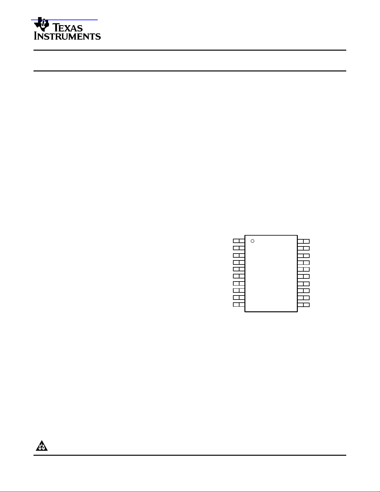
PW PACKAGE
(TOP VIEW)
查询CDC5806供应商
THREE PLLs BASED CLOCK GENERATOR FOR DIGITAL TV APPLICATIONS
FEATURES DESCRIPTION
• High Performance Clock Generator
• Clock Input Compatible With LVCMOS/LVTTL
• Requires a 54-MHz Input Clock to Generate
Multiple Output Frequencies
• Low Jitter for Clock Distribution
• Generates the Following Clocks:
– VIDCLK 74.175824 MHz/54 MHz
(Buffered)
– AUDCLK 16.9344 MHz/12.288 MHz
– CPUCLK 64 MHz
– ASICCLK 32 MHz
– USBCLK 48 MHz
– MCCLK 38.4 MHz/19.2 MHz/12 MHz
• Operates From Single 3.3-V Supply
• Low Peak-to-Peak Period Jitter (150 ps
Max)
• PLLs Are Powered Down, if No Valid REF_IN
Clock (< 5 MHz) is Detected or the
V
is Below 2 V
DD
• PLL Loop Filter Components Integrated
• Packaged in TSSOP (PW) 20-Pin Package
• Industrial Temperature Range -40°C to
85°C Applications
CDC5806
SCAS760A – MARCH 2004 – REVISED JULY 2004
The CDC5806 is a clock generator which synthesizes
video clocks, audio clocks, CPU clock, ASIC clock,
USB clock, and a memory card clock from a 54-MHz
system clock.
Three phase-locked loops (PLLs) are used to
generate the different frequencies from the system
clock. On-chip loop filters and internal feedback
eliminate the need for external components.
Since the CDC5806 is based on PLL circuitry, it
requires a stabilization time to achieve phase-lock of
the PLLs. The PLL stabilization time begins after the
reference clock input has a stable phase and
frequency.
The device operates from a single 3.3-V supply
voltage. The CDC5806 device is characterized for
operation from -40°C to 85°C.
APPLICATIONS
• Digital Television With a Memory Card
Interface
Please be aware that an important notice concerning availability, standard warranty, and use in critical applications of Texas
Instruments semiconductor products and disclaimers thereto appears at the end of this data sheet.
PRODUCTION DATA information is current as of publication date.
Products conform to specifications per the terms of the Texas
Instruments standard warranty. Production processing does not
necessarily include testing of all parameters.
Copyright © 2004, Texas Instruments Incorporated
www.ti.com
REF_IN
VIDSEL
AUDSEL
MCSEL
MUX
VIDCLK
AUDCLK
PLL1VSS
PLL1VDD PLL2VDD PLL3VDD
PLL2VSS PLL3VSS
MUX
CPUCLK
ASICCLK
USBCLK
MCCLK
/4
/6
/3
/5
/10
PLL 2
12.288/16.9344 MHz
PLL 3
192 MHz
PLL3VDD
PLL 1
74.175824 MHz
/16
100 kΩ
LVCMOS
LVCMOS
LVCMOS
LVCMOS
LVCMOS
LVCMOS
100 kΩ
100 kΩ
100 kΩ
100 kΩ
100 kΩ
Power
Down
Logic
CDC5806
SCAS760A – MARCH 2004 – REVISED JULY 2004
These devices have limited built-in ESD protection. The leads should be shorted together or the device
placed in conductive foam during storage or handling to prevent electrostatic damage to the MOS gates.
FUNCTIONAL BLOCK DIAGRAM
2
www.ti.com
SCAS760A – MARCH 2004 – REVISED JULY 2004
Terminal Functions
TERMINAL
NAME NO
REF_IN 2 I LVCMOS Reference frequency input
VIDSEL 1 I LVCMOS VIDSEL select input for VIDCLK. It selects between 74.175824 MHz from PLL1 and buffered
AUDSEL 9 I LVCMOS AUDSEL select input for AUDCLK. It selects between 16.9344 MHz and 12.288 MHz from
MCSEL 10 I LVCMOS MCSEL select input for MCCLK. It selects from 38.4 MHz, 19.2 MHz, and 12 MHz from PLL3,
VIDCLK 4 O LVCMOS VIDCLK output 74.175824 MHz or 54 MHz
AUDCLK 7 O LVCMOS AUDCLK output 16.9344 MHz or 12.288 MHz
CPUCLK 17 O LVCMOS CPUCLK output 64 MHz
ASICCLK 20 O LVCMOS ASICCLK output 32 MHz
USBCLK 14 O LVCMOS USBCLK output 48 MHz
MCCLK 4 O LVCMOS MCCLK output 38.4 MHz / 19.2 MHz / 12 MHz
VDD_PLL1 3 Power 3.3-V supply for PLL1 and VIDCLK
VDD_PLL2 6 Power 3.3-V supply for PLL2 and AUDCLK
VDD_PLL3 13, 16, 19 Power 3.3-V supply for PLL3 and CPUCLK, ASICCLK, USBCLK, and MCCLK
VSS_PLL1 5 Ground Ground for PLL1 and VIDCLK
VSS_PLL2 8 Ground Ground for PLL2 and AUDCLK
VSS_PLL3 12, 15, 18 Ground Ground for PLL3 and CPUCLK, ASICCLK, USBCLK, and MCCLK
TYPE DESCRIPTION
input frequency of 54 MHz, 100k||100k pull to mid-level.
PLL2, 100k||100k pull to mid level.
100k||100k pull to mid level.
CDC5806
FUNCTIONAL DESCRIPTION OF THE LOGIC
Table 1. Select Function for Video, Audio, CPU, ASIC, and USB Clocks
VIDSEL AUDSEL VIDCLK AUDCLK CPUCLK ASICCLK USBCLK Unit
L L 54 (buffered) 12.288 64 32 48 MHz
L M Reserved Reserved 64 32 48 MHz
L H 54 (buffered) 16.9344 64 32 48 MHz
M L Reserved Reserved 64 32 48 MHz
M M Reserved Reserved REFCLK/3 REFCLK/6 REFCLK/4 MHz
M H Reserved Reserved 64 32 48 MHz
H L 74.175824 12.288 64 32 48 MHz
H M Reserved Reserved 64 32 48 MHz
H H 74.175824 16.9344 64 32 48 MHz
MCSEL MCCLK MCCLK if VIDSEL = M and AUDSEL = M UNIT
H 12 MHz REFCLK/16 MHz
M 38.4 MHz REFCLK/5 MHz
L 19.2 MHz REFCLK/10 MHz
Table 2. Select Function for MC Clock
3

www.ti.com
CDC5806
SCAS760A – MARCH 2004 – REVISED JULY 2004
ABSOLUTE MAXIMUM RATINGS
over operating free-air temperature (unless otherwise noted)
Supply voltage range, V
Input voltage range, V
Output voltage range, V
Input current (VI< 0, VI>V
Continuous output current, I
Package thermal impedance,Θ
Storage temperature range T
(1) Stresses beyond those listed under absolute maximum ratings may cause permanent damage to the device. These are stress ratings
only, and functional operation of the device at these or any other conditions beyond those indicated under recommended operating
conditions is not implied. Exposure to absolute-maximum-rated conditions for extended periods may affect device reliability.
(2) The input and output negative voltage ratings may be exceeded if the input and output clamp-current ratings are observed.
(3) The package thermal impedance is calculated in accordance with JESD 51 (no airflow condition) and JEDEC2S1P (high-k board).
DD
(2)
I
(2)
O
) ±20 mA
DD
O
(3)
: TSSOP20 package 104 C/W
JA
stg
(1)
0.5 V to 4.6 V
0.5 V to VDD + 0.5 V
0.5 V to VDD + 0.5 V
±50 mA
65°C to 150°C
RECOMMENDED OPERATING CONDITIONS
MIN NOM MAX UNIT
V
DD
T
A
V
IL
V
I thresh
V
IH
V
IL(L)
V
IM(M)
V
IH(H)
I
OH
I
OL
V
I
C
L
Supply voltage 3 3.3 3.6 V
Operating free-air temperature -40 85 °C
Low-level input voltage REF_IN 0.3 V
Input voltage threshold REF_IN 0.5 V
High-level input voltage REF_IN 0.7 V
DD
DD
Three level input low for control inputs 0.13 V
Three level input mid for control inputs 0.4 V
Three level input high for control inputs 0.87 V
DD
DD
High-level output current LVCMOS -8 mA
Low-level output current LVCMOS 8 mA
Input voltage range LVCMOS 0 3.6 V
Output load LVCMOS 5 10 pF
0.6 V
V
DD
V
V
V
DD
V
DD
V
TIMING REQUIREMENTS
over recommended ranges of supply voltage, load, and operating free-air temperature
PARAMETER MIN NOM MAX UNIT
REF_IN REQUIREMENTS
f
CLK_IN
tr/ t
duty
AUDSEL, VIDSEL, MCSEL REQUIREMENTS
tr/ t
t
1
(1) If VIDSEL and AUDSEL are switched from from one state to another state at the same time, then the CPUCLK, ASICCLK, USBCLK, or
4
LVCMOS REF_IN clock input frequency 54 MHz
Rise and fall time REF_IN signal (20% to 80%) 4 ns
f
Duty cycle of REF_IN (VDD/2) 40% 60%
REF
Rise and fall time (20% to 80%) 4 ns
f
Transitional time between AUDSEL and VIDSEL control pins
(1)
6 ns
MCCLK are affected. This is due to the selected reserved mode with VIDSEL = M and AUDSEL = M. This mode causes the PLL3 to be
bypassed and the REFCLK will be seen with the appropriate divider ratios at the correspondent outputs.

www.ti.com
SCAS760A – MARCH 2004 – REVISED JULY 2004
DEVICE CHARACTERISTICS
over recommended operating free-air temperature range (unless otherwise noted)
PARAMETER TEST CONDITIONS MIN TYP MAX UNIT
OVERALL
I
Supply current Test load 35 45 mA
CC
I
Standby current fIN= 0 MHz, V
CC(ST)
V
Supply voltage threshold for power up control circuit 2 V
PUC
LVCMOS
V
LVCMOS input voltage V
IK
I
REF_IN input current VI= 0 V or V
I
I
SELECT input current VI= 0 V or V
I
V
High-level output voltage V
OH
V
Low-level output voltage V
OL
I
High-level output current V
OH
I
Low-level output current V
OL
= 3 V, II= –18 mA –1.2 V
DD
= MIN to MAX, IOH= –5 mA V
DD
= MIN to MAX, IOL= 5 mA 0.4 V
DD
V
= 3 V, VO= V
DD
= 3.3 V, VO= 1.65 V –35 mA
DD
V
= 3.6 V, VO= 0.4 V –75
DD
V
= 3 V, VO= 0.4 V 5
DD
= 3.3 V, VO= 1.65 V 35 mA
DD
V
= 3.6 V, VO= V
DD
AC
C
Input capacitance (Ref_IN) 2 pF
I
Output accuracy VIDCLK, CPUCLK, ASICCLK,
f
err
USBCLK, MCCLK (38.4 MHz, 19.2 MHz, 12 MHz)
f
Output accuracy AUDCLK (16.9344 MHz, 12.288 MHz) See Note
err
t
PLL start up lock time See Figure 2 0.5 ms
L
t
PLL lock time after frequency change on AUDCLK See Figure 2 0.5 ms
L(ω)
See Note
odc Duty cycle for MCCLK Threshold = VDD/2 47% 50% 53%
Duty cycle for VIDCLK, AUDCLK, CPUCLK, ASICCLK,
odc Threshold = VDD/2 45% 50% 55%
USBCLK
tr/t
Rise and fall time of the output 20%–80% of V
f
VIDCLK
(74.175824 MHz)
CPUCLK (64 MHz) 60 150
USBCLK (48 MHz) 65 150
MCCLK (38.4 MHz) 65 150
t
Peak-to-peak period jitter for 10,000 cycles ps
jit(per)
ASICCLK (32 MHz) 60 150
MCCLK (19.2 MHz) 70 150
AUDCLK (16.9344 MHz) 75 150
AUDCLK (12.288 MHz) 85 150
MCCLK (12 MHz) 65 150
(1) This parameter is assured by design as a result of the chosen settings of the internal dividers in the PLL's.
= 3.6 V 1.1 mA
DD
DD
DD
– 0.4 V
DD
– 0.4 V –5
DD
– 0.4V 75
DD
(1)
(1)
O
CDC5806
±5 µA
±55 µA
±1 ppm
±40 ppm
2 ns
75 150
5

www.ti.com
From Output
of DUT
R = 1 kΩ
R = 1 kΩ
V
DD
CL = 10 pF
Time/ms
f
AUDCLK
/MHz
tL Lock-Up Time
V
DD
/V
V
PUC
Time/ms
Time/ms
Time/ms
f
REF_IN
/MHz
AUDSEL
/V
f = 54 MHz
t
L(ω)
Lock Time
f
target
< 1%
f
target
< 1%
CDC5806
SCAS760A – MARCH 2004 – REVISED JULY 2004
Figure 1. LVCMOS Output Test Load
6
Figure 2. Timing Diagram of PLL Lock Time of Audio Clock

MECHANICAL DATA
MTSS001C – JANUARY 1995 – REVISED FEBRUARY 1999
PW (R-PDSO-G**) PLASTIC SMALL-OUTLINE PACKAGE
14 PINS SHOWN
0,65
1,20 MAX
14
0,30
0,19
8
4,50
4,30
PINS **
7
Seating Plane
0,15
0,05
8
1
A
DIM
14
0,10
6,60
6,20
M
0,10
0,15 NOM
0°–8°
2016
Gage Plane
24
0,25
0,75
0,50
28
A MAX
A MIN
NOTES: A. All linear dimensions are in millimeters.
B. This drawing is subject to change without notice.
C. Body dimensions do not include mold flash or protrusion not to exceed 0,15.
D. Falls within JEDEC MO-153
3,10
2,90
5,10
4,90
5,10
4,90
6,60
6,40
7,90
7,70
9,80
9,60
4040064/F 01/97
POST OFFICE BOX 655303 • DALLAS, TEXAS 75265

IMPORTANT NOTICE
Texas Instruments Incorporated and its subsidiaries (TI) reserve the right to make corrections, modifications,
enhancements, improvements, and other changes to its products and services at any time and to discontinue
any product or service without notice. Customers should obtain the latest relevant information before placing
orders and should verify that such information is current and complete. All products are sold subject to TI’s terms
and conditions of sale supplied at the time of order acknowledgment.
TI warrants performance of its hardware products to the specifications applicable at the time of sale in
accordance with TI’s standard warranty. Testing and other quality control techniques are used to the extent TI
deems necessary to support this warranty . Except where mandated by government requirements, testing of all
parameters of each product is not necessarily performed.
TI assumes no liability for applications assistance or customer product design. Customers are responsible for
their products and applications using TI components. To minimize the risks associated with customer products
and applications, customers should provide adequate design and operating safeguards.
TI does not warrant or represent that any license, either express or implied, is granted under any TI patent right,
copyright, mask work right, or other TI intellectual property right relating to any combination, machine, or process
in which TI products or services are used. Information published by TI regarding third-party products or services
does not constitute a license from TI to use such products or services or a warranty or endorsement thereof.
Use of such information may require a license from a third party under the patents or other intellectual property
of the third party, or a license from TI under the patents or other intellectual property of TI.
Reproduction of information in TI data books or data sheets is permissible only if reproduction is without
alteration and is accompanied by all associated warranties, conditions, limitations, and notices. Reproduction
of this information with alteration is an unfair and deceptive business practice. TI is not responsible or liable for
such altered documentation.
Resale of TI products or services with statements different from or beyond the parameters stated by TI for that
product or service voids all express and any implied warranties for the associated TI product or service and
is an unfair and deceptive business practice. TI is not responsible or liable for any such statements.
Following are URLs where you can obtain information on other Texas Instruments products and application
solutions:
Products Applications
Amplifiers amplifier.ti.com Audio www.ti.com/audio
Data Converters dataconverter.ti.com Automotive www.ti.com/automotive
DSP dsp.ti.com Broadband www.ti.com/broadband
Interface interface.ti.com Digital Control www.ti.com/digitalcontrol
Logic logic.ti.com Military www.ti.com/military
Power Mgmt power.ti.com Optical Networking www.ti.com/opticalnetwork
Microcontrollers microcontroller.ti.com Security www.ti.com/security
Telephony www.ti.com/telephony
Video & Imaging www.ti.com/video
Wireless www.ti.com/wireless
Mailing Address: Texas Instruments
Post Office Box 655303 Dallas, Texas 75265
Copyright 2004, Texas Instruments Incorporated
 Loading...