

CDC536
3.3-V PHASE-LOCK LOOP CLOCK DRIVER
WITH 3-STATE OUTPUTS
SCAS378F – APRIL 1994 – REVISED OCTOBER 1998
1
POST OFFICE BOX 655303 • DALLAS, TEXAS 75265
D
Low-Output Skew for Clock-Distribution
and Clock-Generation Applications
D
Operates at 3.3-V V
CC
D
Distributes One Clock Input to Six Outputs
D
One Select Input Configures Three Outputs
to Operate at One-Half or Double the Input
Frequency
D
No External RC Network Required
D
External Feedback Pin (FBIN) Is Used to
Synchronize the Outputs to the Clock Input
D
Application for Synchronous DRAM,
High-Speed Microprocessor
D
Negative-Edge-Triggered Clear for
Half-Frequency Outputs
D
TTL-Compatible Inputs and Outputs
D
Outputs Drive 50-Ω Parallel-Terminated
Transmission Lines
D
State-of-the-Art
EPIC-ΙΙB
BiCMOS Design
Significantly Reduces Power Dissipation
D
Distributed VCC and Ground Pins Reduce
Switching Noise
D
Packaged in Plastic 28-Pin Shrink Small
Outline Package
description
The CDC536 is a high-performance, low-skew, low-jitter clock driver . It uses a phase-lock loop (PLL) to precisely
align, in both frequency and phase, the clock output signals to the clock input (CLKIN) signal. It is specifically
designed for use with synchronous DRAMs and popular microprocessors operating at speeds from 50 MHz to
100 MHz or down to 25 MHz on outputs configured as half-frequency outputs. The CDC536 operates at 3.3-V
V
CC
and is designed to drive a 50-W transmission line.
The feedback input (FBIN) is used to synchronize the output clocks in frequency and phase to the input clock
(CLKIN). One of the six output clocks must be fed back to FBIN for the PLL to maintain synchronization between
CLKIN and the outputs. The output used as the feedback pin is synchronized to the same frequency as CLKIN.
The Y outputs can be configured to switch in phase and at the same frequency as CLKIN. The select (SEL)
input configures three Y outputs to operate at one-half or double the CLKIN frequency depending on which pin
is fed back to FBIN (see Tables 1 and 2). All output signal duty cycles are adjusted to 50% independent of the
duty cycle at the input clock.
Output-enable (OE
) is provided for output control. When OE is high, the outputs are in the high-impedance state.
When OE
is low, the outputs are active. TEST is used for factory testing of the device and can be use to bypass
the PLL. TEST should be strapped to GND for normal operation.
Unlike many products containing PLLs, the CDC536 does not require external RC networks. The loop filter for
the PLL is included on-chip, minimizing component count, board space, and cost.
Copyright 1998, Texas Instruments Incorporated
PRODUCTION DATA information is current as of publication date.
Products conform to specifications per the terms of Texas Instruments
standard warranty. Production processing does not necessarily include
testing of all parameters.
EPIC-ΙΙB is a trademark of Texas Instruments Incorporated.
Please be aware that an important notice concerning availability, standard warranty, and use in critical applications of
Texas Instruments semiconductor products and disclaimers thereto appears at the end of this data sheet.
1
2
3
4
5
6
7
8
9
10
11
12
13
14
28
27
26
25
24
23
22
21
20
19
18
17
16
15
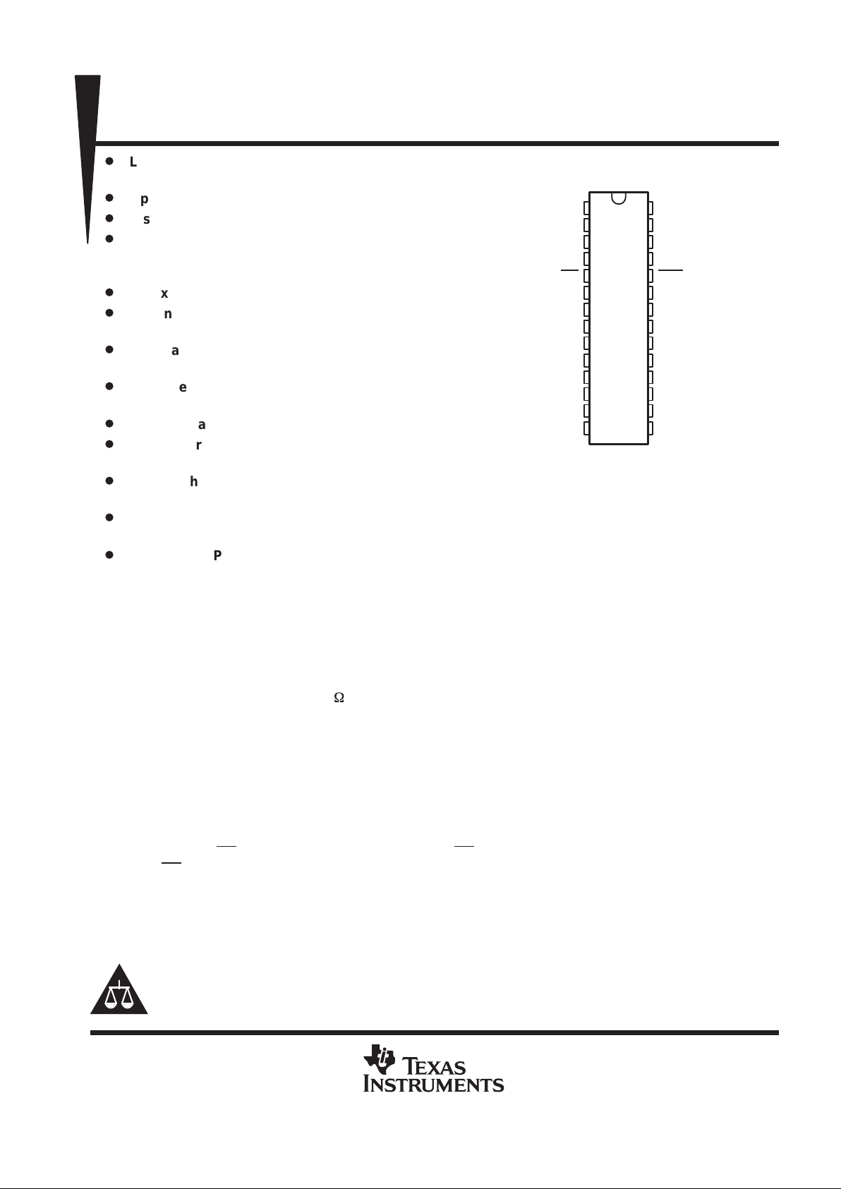
AV
CC
AGND
CLKIN
SEL
OE
GND
1Y1
V
CC
GND
1Y2
V
CC
GND
1Y3
V
CC
AV
CC
AGND
FBIN
TEST
CLR
V
CC
2Y1
GND
V
CC
2Y2
GND
V
CC
2Y3
GND
DB OR DL PACKAGE
(TOP VIEW)
CDC536
3.3-V PHASE-LOCK LOOP CLOCK DRIVER
WITH 3-STATE OUTPUTS
SCAS378F – APRIL 1994 – REVISED OCTOBER 1998
2
POST OFFICE BOX 655303 • DALLAS, TEXAS 75265
description (continued)
Because it is based on PLL circuitry, the CDC536 requires a stabilization time to achieve phase lock of the
feedback signal to the reference signal. This stabilization time is required following power up and application
of a fixed-frequency, fixed-phase signal at CLKIN as well as following any changes to the PLL reference or
feedback signals. Such changes occur upon change of the select inputs, enabling the PLL via TEST , and upon
enable of all outputs via OE
.
The CDC536 is characterized for operation from 0°C to 70°C.
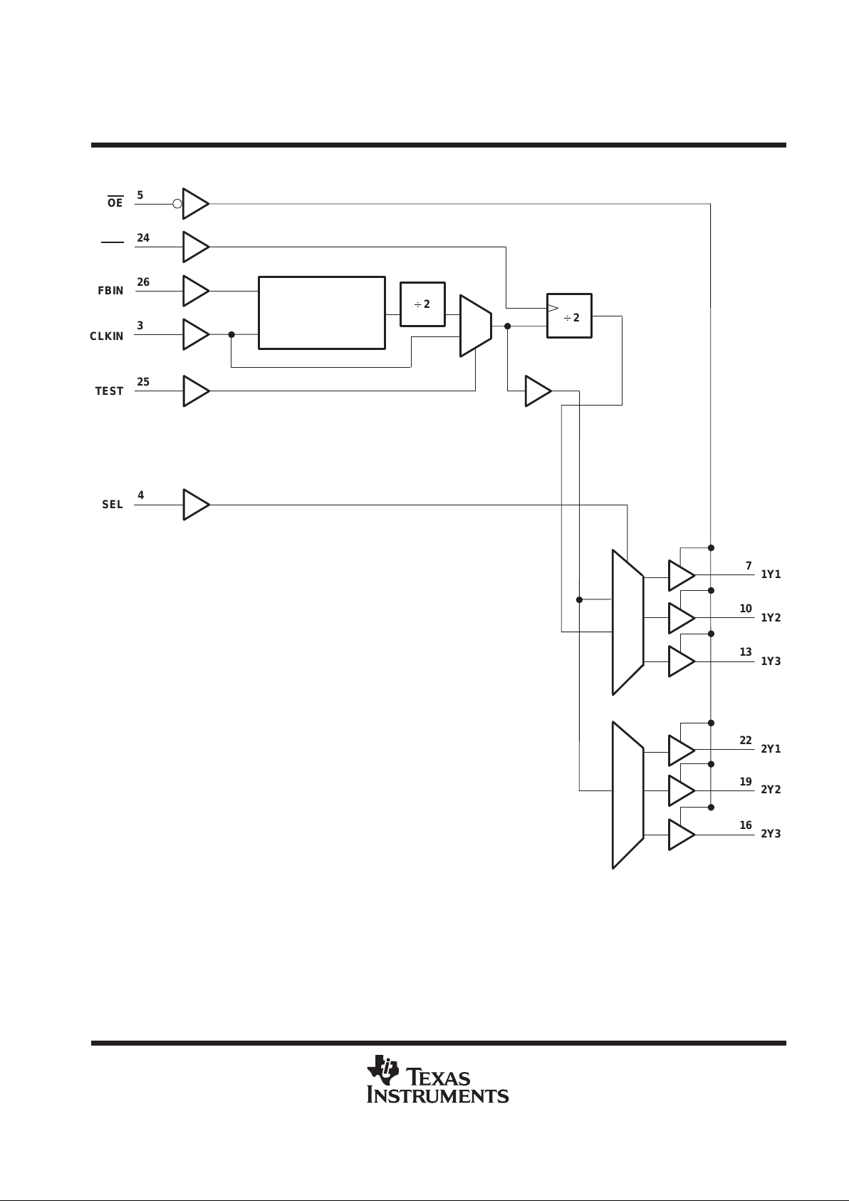
detailed description of output configurations
The voltage-controlled oscillator (VCO) in the CDC536 has a frequency range of 100 MHz to 200 MHz, twice
the operating frequency range of the CDC536 outputs. The output of the VCO is divided by two and by four to
provide reference frequencies with a 50% duty cycle of one-half and one-fourth the VCO frequency . The SEL0
and SEL1 inputs determine which of the two signals are buffered to each bank of device outputs.
One device output must be externally wired to FBIN to complete the PLL. The VCO operates such that the
frequency of this output matches that of the CLKIN signals. In the case that a VCO/2 output is wired to FBIN,
the VCO must operate at twice the CLKIN frequency, resulting in device outputs that operate at the same or
one-half the CLKIN frequency . If a VCO/4 output is wired to FBIN, the device outputs operate at the same or
twice the CLKIN frequency.
output configuration A
Output configuration A is valid when any output configured as a 1× frequency output in Table 1 is fed back to
the FBIN input. The input frequency range for the CLKIN input is 50 MHz to 100 MHz when using output
configuration A. Outputs configured as 1/2× outputs operate at half the CLKIN frequency, while outputs
configured as 1× outputs operate at the same frequency as the CLKIN input.
Table 1. Output Configuration A
INPUTS
OUTPUTS
SEL
1/2×
FREQUENCY1×FREQUENCY
L None All
H 1Yn 2Yn
NOTE: n = 1, 2, 3
output configuration B
Output configuration B is valid when any output configured as a 1× frequency output in Table 2 is fed back to
FBIN. The input frequency range for the CLKIN input is 25 MHz to 50 MHz when using output configuration B.
Outputs configured as 1× outputs operate at the CLKIN frequency, while outputs configured as 2× outputs
operate at double the frequency of the CLKIN input.
Table 2. Output Configuration B
INPUTS
OUTPUTS
SEL
1×
FREQUENCY2×FREQUENCY
L All None
H 1Yn 2Yn
NOTE: n = 1, 2, 3
CDC536
3.3-V PHASE-LOCK LOOP CLOCK DRIVER
WITH 3-STATE OUTPUTS
SCAS378F – APRIL 1994 – REVISED OCTOBER 1998
3
POST OFFICE BOX 655303 • DALLAS, TEXAS 75265
functional block diagram
2Y3
2Y2
2Y1
1Y3
1Y2
1Y1
Phase-Lock Loop
CLR
CLKIN
TEST
SEL
FBIN
OE
B
2
B
2
5
24
26
3
25
4
7
10
13
22
19
16
CDC536
3.3-V PHASE-LOCK LOOP CLOCK DRIVER
WITH 3-STATE OUTPUTS
SCAS378F – APRIL 1994 – REVISED OCTOBER 1998
4
POST OFFICE BOX 655303 • DALLAS, TEXAS 75265
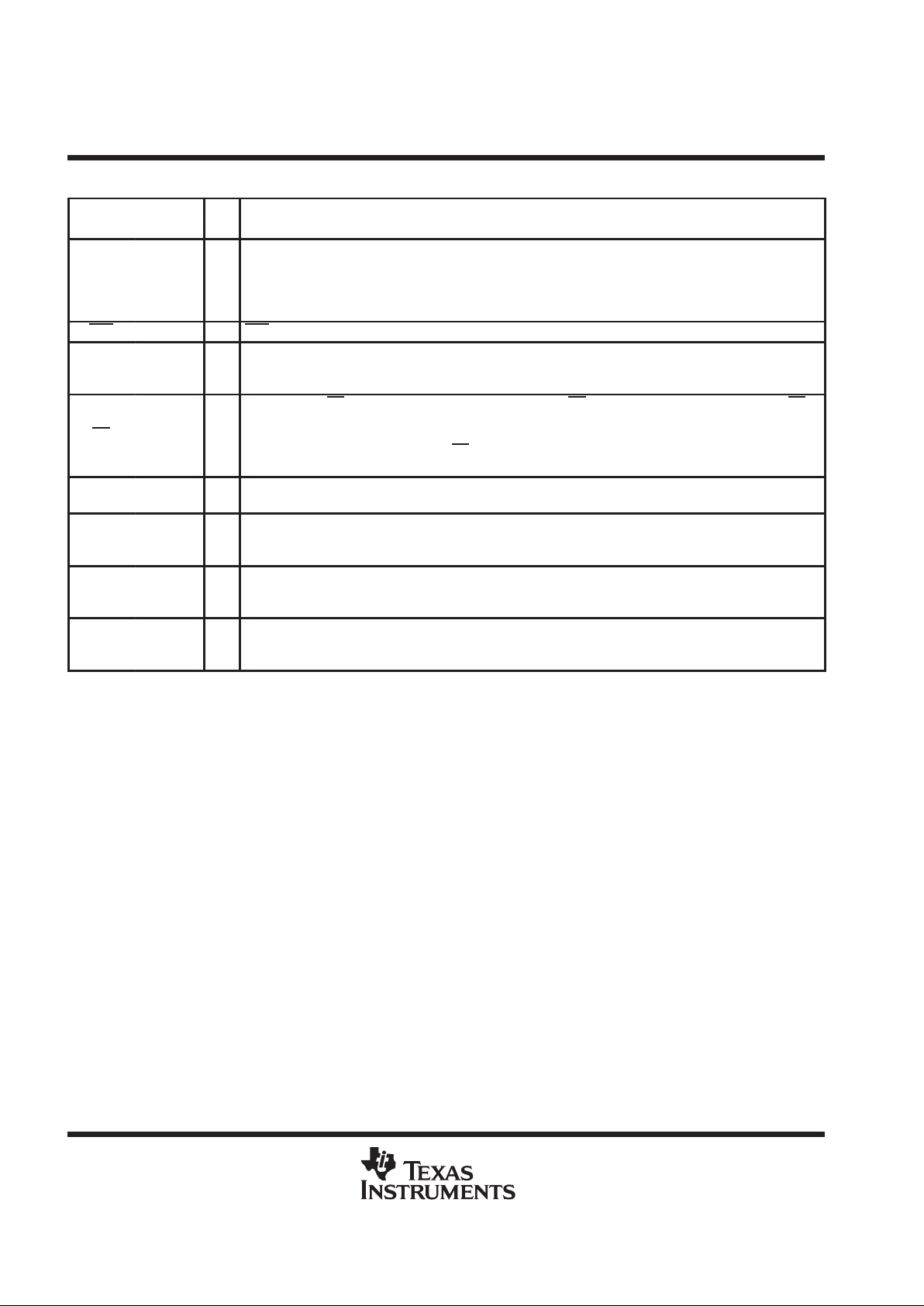
Terminal Functions
TERMINAL
NAME NO.
I/O
DESCRIPTION
CLKIN 3 I
Clock input. CLKIN provides the clock signal to be distributed by the CDC536 clock-driver circuit. CLKIN is used
to provide the reference signal to the integrated phase-lock loop that generates the clock output signals. CLKIN
must have a fixed frequency and fixed phase in order for the phase-lock loop to obtain phase lock. Once the
circuit is powered up and a valid CLKIN signal is applied, a stabilization time is required for the phase-lock loop
to phase lock the feedback signal to its reference signal.
CLR 24 I CLR is used for testing purposes only.
FBIN 26 I
Feedback input. FBIN provides the feedback signal to the internal PLL. FBIN must be hardwired to one of the
six clock outputs to provide frequency and phase lock. The internal PLL adjusts the output clocks to obtain zero
phase delay between the FBIN and differential CLKIN inputs.
OE 5 I
Output enable. OE is the output enable for all outputs. When OE is low, all outputs are enabled. When OE is
high, all outputs are in the high-impedance state. Since the feedback signal for the phase-lock loop is taken
directly from an output, placing the outputs in the high-impedance state interrupts the feedback loop; therefore,
when a high-to-low transition occurs at OE
, enabling the output buffers, a stabilization time is required before
the phase-lock loop obtains phase lock.
SEL 4 I
Output configuration select. SEL selects the output configuration for each output bank (e.g. 1×, 1/2×, or 2×).
(see Tables 1 and 2).
TEST 25 I
TEST is used to bypass the phase-lock loop circuitry for factory testing of the device. When TEST is low, all
outputs operate using the PLL circuitry. When TEST is high, the outputs are placed in a test mode that bypasses
the PLL circuitry. TEST should be grounded for normal operation.
1Y1–1Y3 7, 10, 13 O
These outputs are configured by SEL to transmit one-half or one-fourth the frequency of the VCO. The
relationship between the CLKIN frequency and the output frequency is dependent on SEL. The duty cycle of
the Y output signals is nominally 50%, independent of the duty cycle of the CLKIN signal.
2Y1–2Y3 22, 19, 16 O
These outputs transmit one-half the frequency of the VCO. The relationship between the CLKIN frequency and
the output frequency is dependent on the frequency of the output being fed back to FBIN. The duty cycle of the
Y output signals is nominally 50% independent of the duty cycle of the CLKIN signal.

CDC536
3.3-V PHASE-LOCK LOOP CLOCK DRIVER
WITH 3-STATE OUTPUTS
SCAS378F – APRIL 1994 – REVISED OCTOBER 1998
5
POST OFFICE BOX 655303 • DALLAS, TEXAS 75265
absolute maximum ratings over operating free-air temperature range (unless otherwise noted)
†
Supply voltage range, V
CC
–0.5 V to 4.6 V. . . . . . . . . . . . . . . . . . . . . . . . . . . . . . . . . . . . . . . . . . . . . . . . . . . . . . . . .
Input voltage range, V
I
(see Note 1) –0.5 V to 7 V. . . . . . . . . . . . . . . . . . . . . . . . . . . . . . . . . . . . . . . . . . . . . . . . . .
Voltage range applied to any output in the high state or power-off state, V
O
(see Note 1) –0.5 V to 5.5 V. . .
Current into any output in the low state, I
O
64 mA. . . . . . . . . . . . . . . . . . . . . . . . . . . . . . . . . . . . . . . . . . . . . . . . . .
Input clamp current, I
IK
(V
I
< 0) –20 mA. . . . . . . . . . . . . . . . . . . . . . . . . . . . . . . . . . . . . . . . . . . . . . . . . . . . . . . . . . .
Output clamp current, I
OK
(V
O
< 0) –50 mA. . . . . . . . . . . . . . . . . . . . . . . . . . . . . . . . . . . . . . . . . . . . . . . . . . . . . . . .
Maximum power dissipation at T
A
= 55°C (in still air) (see Note 2):DB package 0.68 W. . . . . . . . . . . . . . . . . . .
DL package 0.7 W. . . . . . . . . . . . . . . . . . . .
Operating free-air temperature range, T
A
0°C to 70°C. . . . . . . . . . . . . . . . . . . . . . . . . . . . . . . . . . . . . . . . . . . . . .
Storage temperature range, T
stg
–65°C to 150°C. . . . . . . . . . . . . . . . . . . . . . . . . . . . . . . . . . . . . . . . . . . . . . . . . . .
†
Stresses beyond those listed under “absolute maximum ratings” may cause permanent damage to the device. These are stress ratings only, and
functional operation of the device at these or any other conditions beyond those indicated under “recommended operating conditions” is not
implied. Exposure to absolute-maximum-rated conditions for extended periods may affect device reliability.
NOTES: 1. The input and output negative-voltage ratings may be exceeded if the input and output clamp-current ratings are observed.
2. The maximum package power dissipation is calculated using a junction temperature of 150°C and a board trace length of 75 mils.
For more information, refer to the
Package Thermal Considerations
application note in the
ABT Advanced BiCMOS T echnology Data
Book
, literature number SCBD002.
recommended operating conditions (see Note 3)
MIN MAX UNIT
V
CC
Supply voltage 3 3.6 V
V
IH
High-level input voltage 2 V
V
IL
Low-level input voltage 0.8 V
V
I
Input voltage 0 5.5 V
I
OH
High-level output current –32 mA
I
OL
Low-level output current 32 mA
T
A
Operating free-air temperature 0 70 °C
NOTE 3: Unused inputs must be held high or low.
electrical characteristics over recommended operating free-air temperature range (unless
otherwise noted)
TA = 25°C
PARAMETER
TEST CONDITIONS
MIN MAX
UNIT
V
IK
VCC = 3 V, II = –18 mA –1.2 V
VCC = MIN to MAX‡, IOH = –100 µA VCC–0.2
V
OH
VCC = 3 V, IOH = – 32 mA 2
V
VCC = 3 V, IOL = 100 µA 0.2
V
OL
VCC = 3 V, IOL = 32 mA 0.5
V
VCC = 0 or MAX‡, VI = 3.6 V ±10
I
I
VCC = 3.6 V, VI = VCC or GND ±1
µ
A
I
OZH
VCC = 3.6 V, VO = 3 V 10 µA
I
OZL
VCC = 3.6 V, VO = 0 –10 µA
Outputs high 2
I
CC
VCC = 3.6 V, IO = 0,
Outputs low 2
mA
V
I
=
V
CC
or
GND
Outputs disabled 2
C
i
VI = VCC or GND 6 pF
C
o
VO = VCC or GND 9 pF
‡
For conditions shown as MIN or MAX, use the appropriate value specified under recommended operating conditions.

CDC536
3.3-V PHASE-LOCK LOOP CLOCK DRIVER
WITH 3-STATE OUTPUTS
SCAS378F – APRIL 1994 – REVISED OCTOBER 1998
6
POST OFFICE BOX 655303 • DALLAS, TEXAS 75265
timing requirements over recommended ranges of supply voltage and operating free-air
temperature
MIN MAX UNIT
When VCO is operating at four times the CLKIN frequency 25 50
f
clock
Clock frequenc
y
When VCO is operating at double the CLKIN frequency
50 100
MH
z
Input clock duty cycle 40% 60%
After SEL 50
After OE↓ 50
Stabilization time
†
After power up 50
µ
s
After CLKIN 50
†
Time required for the integrated PLL circuit to obtain phase lock of its feedback signal to its reference signal. In order for phase lock to be obtained,
a fixed-frequency, fixed-phase reference signal must be present at CLKIN. Until phase lock is obtained, the specifications for propagation delay
and skew parameters given in the switching characteristics table are not applicable.
switching characteristics over recommended ranges of supply voltage and operating free-air
temperature, C
L
= 30 pF (see Note 4 and Figures 1 and 2)
PARAMETER
FROM
(INPUT)
TO
(OUTPUT)
MIN MAX UNIT
f
max
100 MHz
Duty cycle Y 45% 55%
t
phase error
‡
CLKIN↑ Y –500 +500 ps
Jitter
(pk-pk)
CLKIN↑ Y 200 ps
t
sk(o)
‡
0.5 ns
t
sk(pr)
1 ns
t
r
1.4 ns
t
f
1.4 ns
‡
The propagation delay, t
phase error
, is dependent on the feedback path from any output to FBIN. The t
phase error
, t
sk(o)
, and t
sk(pk)
specifications
are only valid for equal loading of all outputs.
NOTE 4: The specifications for parameters in this table are applicable only after any appropriate stabilization time has elapsed.

CDC536
3.3-V PHASE-LOCK LOOP CLOCK DRIVER
WITH 3-STATE OUTPUTS
SCAS378F – APRIL 1994 – REVISED OCTOBER 1998
7
POST OFFICE BOX 655303 • DALLAS, TEXAS 75265
PARAMETER MEASUREMENT INFORMATION
From Output
Under Test
LOAD CIRCUIT FOR OUTPUTS
CL = 30 pF
(see note A)
VOLTAGE WAVEFORMS
PROPAGATION DELAY TIMES
t
phase error
1.5 V 1.5 V
3 V
0 V
1.5 V
V
OH
V
OL
Input
0.8 V
2 V
t
r
t
f
0.8 V
2 V
Output
500
W
NOTES: A. CL includes probe and jig capacitance.
B. All input pulses are supplied by generators having the following characteristics: PRR ≤ 100 MHz, ZO = 50 Ω, tr ≤ 2.5 ns, tf≤ 2.5 ns.
C. The outputs are measured one at a time with one transition per measurement.
Figure 1. Load Circuit and Voltage Waveforms
CDC536
3.3-V PHASE-LOCK LOOP CLOCK DRIVER
WITH 3-STATE OUTPUTS
SCAS378F – APRIL 1994 – REVISED OCTOBER 1998
8
POST OFFICE BOX 655303 • DALLAS, TEXAS 75265
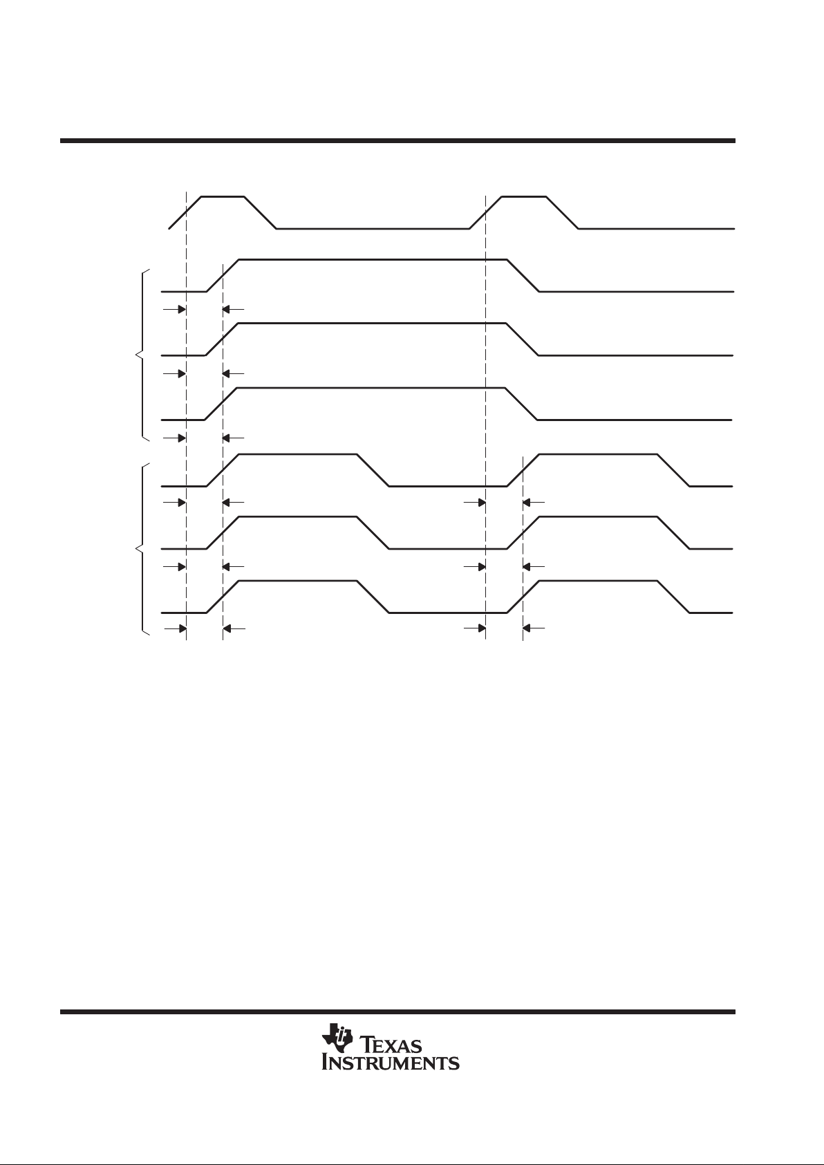
PARAMETER MEASUREMENT INFORMATION
t
phase error 1
CLKIN
Outputs
Operating
at 1/2 CLKIN
Frequency
Outputs
Operating
at CLKIN
Frequency
t
phase error 2
t
phase error 3
t
phase error 4
t
phase error 5
t
phase error 6
t
phase error 7
t
phase error 8
t
phase error 9
NOTES: A. Output skew, t
sk(o)
, is calculated as the greater of:
– The difference between the fastest and slowest of t
phase error n
(n = 1, 2,...6)
– The difference between the fastest and slowest of t
phase error n
(n = 7, 8, 9)
B. Process skew, t
sk(pr)
, is calculated as the greater of:
– The difference between the maximum and minimum t
phase error n
(n = 1, 2,...6) across multiple devices under identical
operating conditions.
– The difference between the maximum and minimum t
phase error n
(n = 7, 8, 9) across multiple devices under identical
operating conditions.
Figure 2. Skew Waveforms and Calculations

CDC536
3.3-V PHASE-LOCK LOOP CLOCK DRIVER
WITH 3-STATE OUTPUTS
SCAS378F – APRIL 1994 – REVISED OCTOBER 1998
9
POST OFFICE BOX 655303 • DALLAS, TEXAS 75265
PARAMETER MEASUREMENT INFORMATION
t
phase error 10
t
phase error 11
t
phase error 12
t
phase error 15
CLKIN
Outputs
Operating
at CLKIN
Frequency
Outputs
Operating
at 2× CLKIN
Frequency
t
phase error 13
t
phase error 14
NOTES: A. Output skew, t
sk(o)
, is calculated as the greater of:
– The difference between the fastest and slowest of t
phase error n
(n = 10, 11,...15)
B. Process skew, t
sk(pr)
, is calculated as the greater of:
– The difference between the maximum and minimum t
phase error n
(n = 10, 11,. . . 15) across multiple devices under identical
operating conditions.
Figure 3. Waveforms for Calculation of t
sk(o)
and t
sk(pr)
CDC536
3.3-V PHASE-LOCK LOOP CLOCK DRIVER
WITH 3-STATE OUTPUTS
SCAS378F – APRIL 1994 – REVISED OCTOBER 1998
10
POST OFFICE BOX 655303 • DALLAS, TEXAS 75265
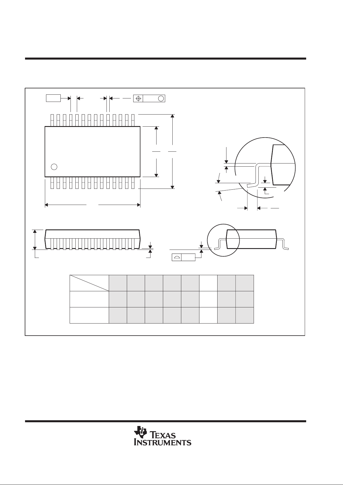
MECHANICAL INFORMATION
DB (R-PDSO-G**) PLASTIC SMALL-OUTLINE PACKAGE
4040065 /C 10/95
28 PIN SHOWN
Gage Plane
8,20
7,40
0,15 NOM
0,63
1,03
0,25
38
12,90
12,30
28
10,50
24
8,50
Seating Plane
9,907,90
30
10,50
9,90
0,38
5,60
5,00
15
0,22
14
A
28
1
2016
6,50
6,50
14
0,05 MIN
5,905,90
DIM
A MAX
A MIN
PINS **
2,00 MAX
6,90
7,50
0,65
M
0,15
0°–8°
0,10
3,30
8
2,70
NOTES: A. All linear dimensions are in millimeters.
B. This drawing is subject to change without notice.
C. Body dimensions do not include mold flash or protrusion not to exceed 0,15.
D. Falls within JEDEC MO-150

CDC536
3.3-V PHASE-LOCK LOOP CLOCK DRIVER
WITH 3-STATE OUTPUTS
SCAS378F – APRIL 1994 – REVISED OCTOBER 1998
11
POST OFFICE BOX 655303 • DALLAS, TEXAS 75265
MECHANICAL INFORMATION
DL (R-PDSO-G**) PLASTIC SMALL-OUTLINE PACKAGE
4040048/C 03/97
48 PIN SHOWN
56
0.730
(18,54)
0.720
(18,29)
4828
0.370
(9,40)
(9,65)
0.380
Gage Plane
DIM
0.420 (10,67)
0.395 (10,03)
A MIN
A MAX
0.006 (0,15) NOM
PINS **
0.630
(16,00)
(15,75)
0.620
0.010 (0,25)
Seating Plane
0.020 (0,51)
0.040 (1,02)
25
24
0.008 (0,203)
0.012 (0,305)
48
1
0.008 (0,20) MIN
A
0.110 (2,79) MAX
0.299 (7,59)
0.291 (7,39)
0.004 (0,10)
M
0.005 (0,13)
0.025 (0,635)
0°–8°
NOTES: A. All linear dimensions are in inches (millimeters).
B. This drawing is subject to change without notice.
C. Body dimensions do not include mold flash or protrusion not to exceed 0.006 (0,15).
D. Falls within JEDEC MO-118

IMPORTANT NOTICE
T exas Instruments and its subsidiaries (TI) reserve the right to make changes to their products or to discontinue
any product or service without notice, and advise customers to obtain the latest version of relevant information
to verify, before placing orders, that information being relied on is current and complete. All products are sold
subject to the terms and conditions of sale supplied at the time of order acknowledgement, including those
pertaining to warranty, patent infringement, and limitation of liability.
TI warrants performance of its semiconductor products to the specifications applicable at the time of sale in
accordance with TI’s standard warranty. Testing and other quality control techniques are utilized to the extent
TI deems necessary to support this warranty. Specific testing of all parameters of each device is not necessarily
performed, except those mandated by government requirements.
CERT AIN APPLICATIONS USING SEMICONDUCTOR PRODUCTS MAY INVOLVE POTENTIAL RISKS OF
DEATH, PERSONAL INJURY, OR SEVERE PROPERTY OR ENVIRONMENTAL DAMAGE (“CRITICAL
APPLICATIONS”). TI SEMICONDUCTOR PRODUCTS ARE NOT DESIGNED, AUTHORIZED, OR
WARRANTED TO BE SUITABLE FOR USE IN LIFE-SUPPORT DEVICES OR SYSTEMS OR OTHER
CRITICAL APPLICATIONS. INCLUSION OF TI PRODUCTS IN SUCH APPLICA TIONS IS UNDERST OOD TO
BE FULLY AT THE CUSTOMER’S RISK.
In order to minimize risks associated with the customer’s applications, adequate design and operating
safeguards must be provided by the customer to minimize inherent or procedural hazards.
TI assumes no liability for applications assistance or customer product design. TI does not warrant or represent
that any license, either express or implied, is granted under any patent right, copyright, mask work right, or other
intellectual property right of TI covering or relating to any combination, machine, or process in which such
semiconductor products or services might be or are used. TI’s publication of information regarding any third
party’s products or services does not constitute TI’s approval, warranty or endorsement thereof.
Copyright 1998, Texas Instruments Incorporated
 Loading...