

查询CDC516供应商
CDC516
3.3-V PHASE-LOCK LOOP CLOCK DRIVER
SCAS575A – JULY 1996 – REVISED JANUAR Y 1998
D
Phase-Lock Loop Clock Distribution for
Synchronous DRAM Applications
D
Distributes One Clock Input to Four Banks
of Four Outputs
D
Separate Output Enable for Each Output
Bank
D
External Feedback Pin (FBIN) Is Used to
Synchronize the Outputs to the Clock Input
D
No External RC Network Required
D
Operates at 3.3-V V
D
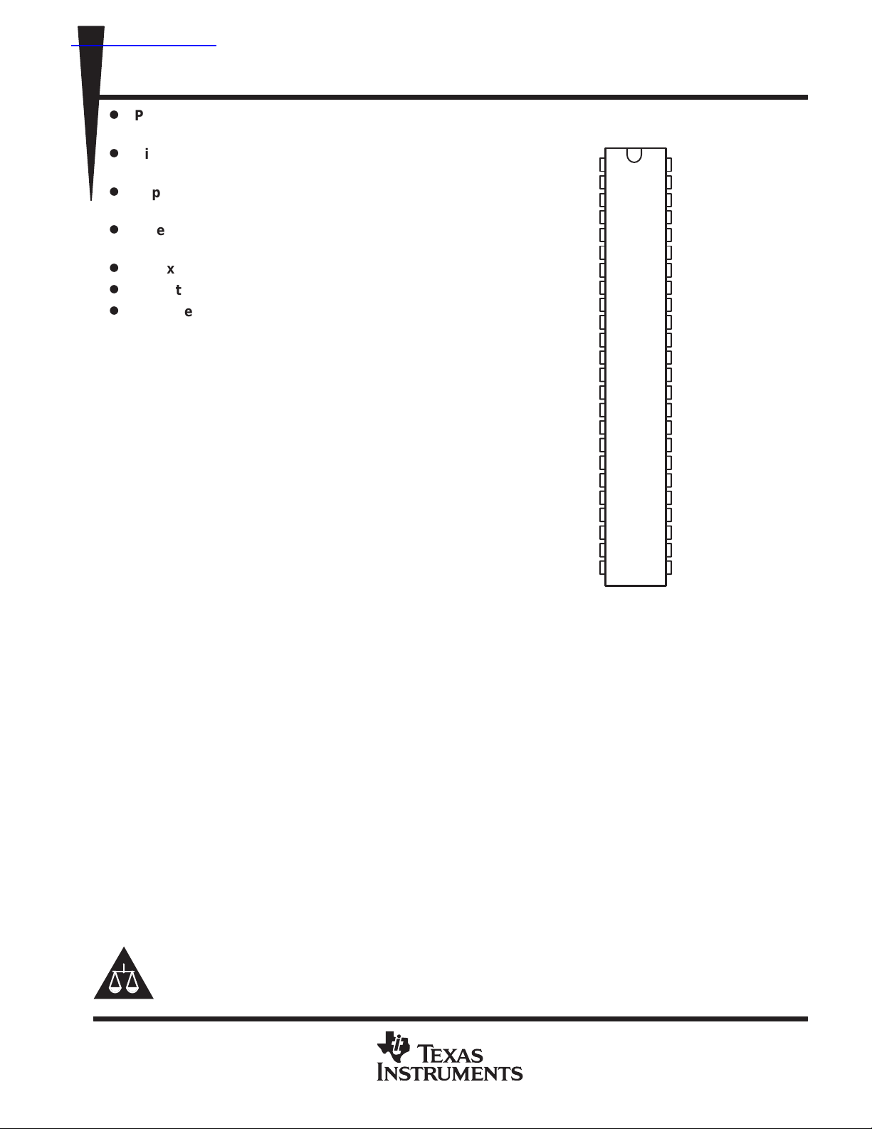
Packaged in Plastic 48-Pin Thin Shrink
Small-Outline Package
CC
description
The CDC516 is a high-performance, low-skew,
low-jitter, phase-lock loop clock driver. It uses a
phase-lock loop (PLL) to precisely align, in both
frequency and phase, the feedback output
(FBOUT) to the clock (CLK) input signal. It is
specifically designed for use with synchronous
DRAMs. The CDC516 operates at 3.3-V V
is designed to drive up to five clock loads per
output.
Four banks of four outputs provide 16 low-skew,
low-jitter copies of the input clock. Output signal
duty cycles are adjusted to 50 percent,
independent of the duty cycle at the input clock.
Each bank of outputs can be enabled or disabled
separately via the 1G, 2G, 3G, and 4G control
inputs. When the G inputs are high, the outputs
switch in phase and frequency with CLK; when the
G inputs are low, the outputs are disabled to the
logic-low state.
CC
and
V
CC
1Y0
1Y1
GND
GND
1Y2
1Y3
V
CC
1G
GND
AV
CC
CLK
AGND
AGND
GND
2G
V
CC
2Y0
2Y1
GND
GND
2Y2
2Y3
V
CC
DGG PACKAGE
(TOP VIEW)
1
48
2
47
3
46
4
45
5
44
6
43
7
42
8
41
9
40
10
39
11
38
12
37
13
36
14
35
15
34
16
33
17
32
18
31
19
30
20
29
21
28
22
27
23
26
24
25
V
CC
4Y0
4Y1
GND
GND
4Y2
4Y3
V
CC
4G
GND
AV
CC
FBIN
AGND
FBOUT
GND
3G
V
CC
3Y0
3Y1
GND
GND
3Y2
3Y3
V
CC
Unlike many products containing PLLs, the CDC516 does not require external RC networks. The loop filter for
the PLL is included on-chip, minimizing component count, board space, and cost.
Because it is based on PLL circuitry, the CDC516 requires a stabilization time to achieve phase lock of the
feedback signal to the reference signal. This stabilization time is required following power up and application
of a fixed-frequency, fixed-phase signal at CLK, as well as following any changes to the PLL reference or
feedback signals. The PLL may be bypassed for test purposes by strapping AV
to ground.
CC
The CDC516 is characterized for operation from 0°C to 70°C.
Please be aware that an important notice concerning availability, standard warranty, and use in critical applications of
Texas Instruments semiconductor products and disclaimers thereto appears at the end of this data sheet.
PRODUCTION DATA information is current as of publication date.
Products conform to specifications per the terms of Texas Instruments
standard warranty. Production processing does not necessarily include
testing of all parameters.
POST OFFICE BOX 655303 • DALLAS, TEXAS 75265
Copyright 1998, Texas Instruments Incorporated
1
CDC516
3.3-V PHASE-LOCK LOOP CLOCK DRIVER
SCAS575A – JULY 1996 – REVISED JANUAR Y 1998
FUNCTION TABLE
INPUTS
1G 2G 3G 4G CLK
X X X X L L L L L L
L LLLHLLLL H
L LLHHLLLHH
L LHLHLLHL H
L LHHHLLHHH
L HLLHLHLL H
L HLHHLHLHH
L HHLHLHHL H
L HHHHLHHH H
H LLLHHLLLH
H LLHHHLLH H
H LHLHHLHL H
H LHHHHLHH H
H HLLHHHLL H
H HLHHHHLH H
H HHLHHHHL H
H H H H H H H H H H
OUTPUTS
1Y
(0:3)2Y(0:3)3Y(0:3)4Y(0:3)
FBOUT
AVAILABLE OPTIONS
PACKAGE
T
A
0°C to 70°C CDC516DGGR
SMALL OUTLINE
(PW)
2
POST OFFICE BOX 655303 • DALLAS, TEXAS 75265
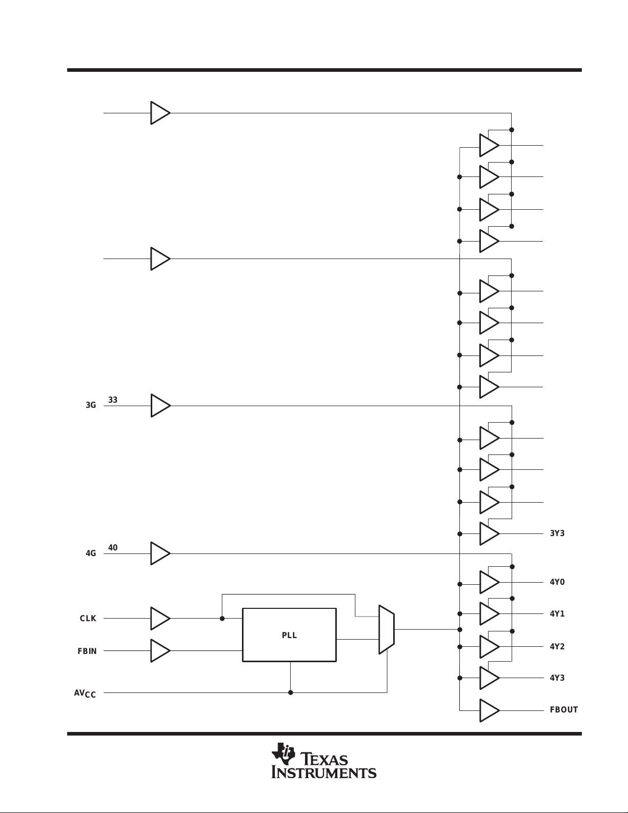
functional block diagram
9
1G
16
2G
CDC516
3.3-V PHASE-LOCK LOOP CLOCK DRIVER
SCAS575A – JULY 1996 – REVISED JANUAR Y 1998
2
1Y0
3
1Y1
6
1Y2
7
1Y3
18
2Y0
19
2Y1
3G
4G
CLK
FBIN
33
40
12
37
PLL
22
23
31
30
27
26
47
46
43
2Y2
2Y3
3Y0
3Y1
3Y2
3Y3
4Y0
4Y1
4Y2
AV
CC
42
35
4Y3
FBOUT
3
11
POST OFFICE BOX 655303 • DALLAS, TEXAS 75265
CDC516
TYPE
DESCRIPTION
3.3-V PHASE-LOCK LOOP CLOCK DRIVER
SCAS575A – JULY 1996 – REVISED JANUAR Y 1998
Terminal Functions
TERMINAL
NAME NO.
Clock input. CLK provides the clock signal to be distributed by the CDC516 clock driver. CLK is used
to provide the reference signal to the integrated PLL that generates the clock output signals. CLK must
CLK 12 I
FBIN 37 I
1G 9 I
2G 16 I
3G 33 I
4G 40 I
FBOUT 35 O
1Y(0:3) 2, 3, 6, 7 O
2Y(0:3) 18, 19, 22, 26 O
3Y(0:3) 31, 30, 27, 26 O
4Y(0:3) 47, 46, 43, 42 O
AV
CC
AGND 13, 14, 36 Ground Analog ground. AGND provides the ground reference for the analog circuitry.
V
CC
GND
11, 38 Power
1, 8, 17, 24,
25, 32, 41, 48
4, 5, 10, 15,
20, 21, 28, 29,
34, 39, 44, 45
Power Power supply
Ground Ground
have a fixed frequency and fixed phase for the PLL to obtain phase lock. Once the circuit is powered
up and a valid CLK signal is applied, a stabilization time is required for the PLL to phase lock the
feedback signal to its reference signal.
Feedback input. FBIN provides the feedback signal to the internal PLL. FBIN must be hard-wired to
FBOUT to complete the PLL. The integrated PLL synchronizes CLK and FBIN so that there is
nominally zero phase error between CLK and FBIN.
Output bank enable. 1G is the output enable for outputs 1Y(0:3). When 1G is low, outputs 1Y(0:3) are
disabled to a logic-low state. When 1G is high, all outputs 1Y(0:3) are enabled and switch at the same
frequency as CLK.
Output bank enable. 2G is the output enable for outputs 2Y(0:3). When 2G is low, outputs 2Y(0:3) are
disabled to a logic-low state. When 2G is high, all outputs 2Y(0:3) are enabled and switch at the same
frequency as CLK.
Output bank enable. 3G is the output enable for outputs 3Y(0:3). When 3G is low, outputs 3Y(0:3) are
disabled to a logic-low state. When 3G is high, all outputs 3Y(0:3) are enabled and switch at the same
frequency as CLK.
Output bank enable. 4G is the output enable for outputs 4Y(0:3). When 4G is low, outputs 4Y(0:3) are
disabled to a logic-low state. When 4G is high, all outputs 4Y(0:3) are enabled and switch at the same
frequency as CLK.
Feedback output. FBOUT is dedicated for external feedback. It switches at the same frequency as
CLK. When externally wired to FBIN, FBOUT completes the feedback loop of the PLL.
Clock outputs. These outputs provide low-skew copies of CLK. Outputs 1Y(0:3) are enabled via 1G.
These outputs can be disabled to a logic-low state by deasserting the 1G control input.
Clock outputs. These outputs provide low-skew copies of CLK. Outputs 2Y(0:3) are enabled via 2G.
These outputs can be disabled to a logic-low state by deasserting the 2G control input.
Clock outputs. These outputs provide low-skew copies of CLK. Outputs 3Y(0:3) are enabled via 3G.
These outputs can be disabled to a logic-low state by deasserting the 3G control input.
Clock outputs. These outputs provide low-skew copies of CLK. Outputs 4Y(0:3) are enabled via 4G.
These outputs can be disabled to a logic-low state by deasserting the 4G control input.
Analog power supply . A VCC provides the power reference for the analog circuitry. In addition, A V
can be used to bypass the PLL for test purposes. When AVCC is strapped to ground, the PLL is
bypassed and CLK is buffered directly to the device outputs.
CC
4
POST OFFICE BOX 655303 • DALLAS, TEXAS 75265

V
V
V
V
CDC516
3.3-V PHASE-LOCK LOOP CLOCK DRIVER
SCAS575A – JULY 1996 – REVISED JANUAR Y 1998
absolute maximum ratings over operating free-air temperature range (unless otherwise noted)
Supply voltage range, V
Input voltage range, VI (see Note 1) –0.5 V to 6.5 V. . . . . . . . . . . . . . . . . . . . . . . . . . . . . . . . . . . . . . . . . . . . . . . . .
Voltage range applied to any output in the high
or low state, VO (see Notes 1 and 2) –0.5 V to VCC + 0.5 V. . . . . . . . . . . . . . . . . . . . . . . . . . . . . . . . . . . . . . . . . .
Input clamp current, I
Output clamp current, I
Continuous output current, I
Continuous current through each VCC or GND ±100 mA. . . . . . . . . . . . . . . . . . . . . . . . . . . . . . . . . . . . . . . . . . . . .
Maximum power dissipation at TA = 55°C (in still air) (see Note 3) 0.85 W. . . . . . . . . . . . . . . . . . . . . . . . . . . . . .
Storage temperature range, T
†
Stresses beyond those listed under “absolute maximum ratings” may cause permanent damage to the device. These are stress ratings only, and
functional operation of the device at these or any other conditions beyond those indicated under “recommended operating conditions” is not
implied. Exposure to absolute-maximum-rated conditions for extended periods may affect device reliability.
NOTES: 1. The input and output negative-voltage ratings may be exceeded if the input and output clamp-current ratings are observed.
2. This value is limited to 4.6 V maximum.
3. The maximum package power dissipation is calculated using a junction temperature of 150°C and a board trace length of 750 mils.
For more information, refer to the
Book
, literature number SCBD002.
–0.5 V to 4.6 V. . . . . . . . . . . . . . . . . . . . . . . . . . . . . . . . . . . . . . . . . . . . . . . . . . . . . . . . .
CC
(V
< 0) –50 mA. . . . . . . . . . . . . . . . . . . . . . . . . . . . . . . . . . . . . . . . . . . . . . . . . . . . . . . . . . .
IK
I
(V
OK
< 0 or VO > VCC) ±50 mA. . . . . . . . . . . . . . . . . . . . . . . . . . . . . . . . . . . . . . . . . . . .
O
(V
= 0 to VCC) ±50 mA. . . . . . . . . . . . . . . . . . . . . . . . . . . . . . . . . . . . . . . . . . . . . .
O
O
–65°C to 150°C. . . . . . . . . . . . . . . . . . . . . . . . . . . . . . . . . . . . . . . . . . . . . . . . . . .
stg
Package Thermal Considerations
application note in the
ABT Advanced BiCMOS T echnology Data
recommended operating conditions (see Note 4)
MIN MAX UNIT
V
V
V
V
I
OH
I
OL
T
NOTE 4: Unused inputs must be held high or low to prevent them from floating.
Supply voltage 3 3.6 V
CC
High-level input voltage 2 V
IH
Low-level input voltage 0.8 V
IL
Input voltage 0 V
I
High-level output current –20 mA
Low-level output current 20 mA
Operating free-air temperature 0 70 °C
A
CC
V
†
electrical characteristics over recommended operating free-air temperature range (unless
otherwise noted)
PARAMETER TEST CONDITIONS V
V
IK
OH
OL
I
I
§
I
CC
∆I
CC
C
i
C
‡
§
o
For conditions shown as MIN or MAX, use the appropriate value specified under recommended operating conditions.
For ICC of AVCC, see Figure 5. For dynamic digital ICC, see Figure 6.
II = –18 mA 3 V –1.2 V
IOH = –100 µA MIN to MAX VCC–0.2
IOH = –20 mA 3 V 2.4
IOL = 100 µA MIN to MAX 0.2
IOL = 20 mA 3 V 0.55
VI = VCC or GND 3.6 V ±5 µA
VI = VCC or GND IO = 0, Outputs: low or high 3.6 V 20 µA
One input at VCC – 0.6 V, Other inputs at VCC or GND 3.3 V to 3.6 V 500 µA
VI = VCC or GND 3.3 V 4 pF
VO = VCC or GND 3.3 V 6 pF
CC
MIN TYP‡MAX UNIT
POST OFFICE BOX 655303 • DALLAS, TEXAS 75265
5

CDC516
(INPUT)
(OUTPUT)
Duty cycle
3.3-V PHASE-LOCK LOOP CLOCK DRIVER
SCAS575A – JULY 1996 – REVISED JANUAR Y 1998
timing requirements over recommended ranges of supply voltage and operating free-air
temperature
MIN MAX UNIT
f
clock
†
Time required for the integrated PLL circuit to obtain phase lock of its feedback signal to its reference signal. For phase lock to be obtained, a
fixed-frequency , fixed-phase reference signal must be present at CLK. Until phase lock is obtained, the specifications for propagation delay, skew ,
and jitter parameters given in the switching characteristics table are not applicable.
Clock frequency 25 125 MHz
Input clock duty cycle 40% 60%
Stabilization time
†
1 ms
switching characteristics over recommended ranges of supply voltage and operating free-air
temperature, C
PARAMETER
t
phase error
reference
(see Figure 3)
t
phase error
‡
These parameters are not production tested.
§
The t
NOTES: 5. The specifications for parameters in this table are applicable only after any appropriate stabilization time has elapsed.
, – jitter,
(see Note 6)
§
t
sk(o)
Jitter
(pk-pk)
t
r
t
f
specification is only valid for equal loading of all outputs.
sk(o)
6. Phase error does not include jitter. The total phase error is 70 ps to 460 ps for the 5% VCC range.
= 30 pF (see Note 5 and Figures 1 and 2)
L
FROM
66 MHz < CLKIN↑ < 100 MHz FBIN↑ –80...400 ps
CLKIN↑ = 100 MHz FBIN↑ 170 360 240 ps
Any Y or FBOUT Any Y or FBOUT 200 ps
F(clkin > 66 MHz) Any Y or FBOUT –100 100 ps
F(clkin ≤ 66 MHz) Any Y or FBOUT 45% 55%
F(clkin > 66 MHz) Any Y or FBOUT 43% 57%
TO
Any Y or FBOUT 1.1 1.5 0.7 1.6 ns
Any Y or FBOUT 0.8 1.3 0.5 1.5 ns
‡
VCC = 3.3 V
± 0.165 V
MIN TYP MAX MIN TYP MAX
VCC = 3.3 V
± 0.3 V
UNIT
6
POST OFFICE BOX 655303 • DALLAS, TEXAS 75265

From Output
Under Test
3.3-V PHASE-LOCK LOOP CLOCK DRIVER
SCAS575A – JULY 1996 – REVISED JANUAR Y 1998
PARAMETER MEASUREMENT INFORMATION
30 pF
500
Input
W
Output
50% V
CC
t
pd
t
r
2 V
0.4 V
50% V
CC
t
f
50% V
2 V
CC
0.4 V
CDC516
3 V
0 V
V
OH
V
OL
LOAD CIRCUIT
NOTES: A. CL includes probe and jig capacitance.
B. All input pulses are supplied by generators having the following characteristics: PRR ≤ 100 MHz, ZO = 50 Ω, tr ≤ 1.2 ns, tf≤ 1.2 ns.
C. The outputs are measured one at a time with one transition per measurement.
Figure 1. Load Circuit and Voltage Waveforms
VOLTAGE WAVEFORMS
PROPAGATION DELA Y TIMES
POST OFFICE BOX 655303 • DALLAS, TEXAS 75265
7

CDC516
3.3-V PHASE-LOCK LOOP CLOCK DRIVER
SCAS575A – JULY 1996 – REVISED JANUAR Y 1998
PARAMETER MEASUREMENT INFORMATION
CLKIN
FBIN
t
phase error
FBOUT
Any Y
Any Y
Any Y
t
sk(o)
t
sk(o)
Figure 2. Phase Error and Skew Calculations
8
POST OFFICE BOX 655303 • DALLAS, TEXAS 75265

CDC516
3.3-V PHASE-LOCK LOOP CLOCK DRIVER
SCAS575A – JULY 1996 – REVISED JANUAR Y 1998
TYPICAL CHARACTERISTICS
PHASE ERROR
CLOCK FREQUENCY
50
VDD = 3.3 V
40
TA = 25°C
30
20
10
0
–10
Phase Error – ps
–20
–30
–40
–50
35
55 95
f
– Clock Frequency – MHz
clk
Figure 3
ANALOG SUPPLY CURRENT
CLOCK FREQUENCY
9
VDD = 3.3 V
8
TA = 25°C
7
6
5
4
3
2
Analog Supply Current – mA
vs
75 115 135
vs
OUTPUT DUTY CYCLE
CLOCK FREQUENCY
57%
VDD = 3.3 V
55%
53%
51%
49%
Output Duty Cycle
47%
45%
43%
CL = 30 pF
50 70 110
f
– Clock Frequency – MHz
clk
Figure 4
DYNAMIC SUPPLY CURRENT
CLOCK FREQUENCY
500
VCC = 3.6 V
450
Bias = 0/3 V
CL = 30 pF to GND
400
TA = 25°C
350
300
250
200
150
Dynamic Supply Current – mA
100
vs
90 13030
vs
1
0
25
35 45 55 85 95
65 105 115 125
f
– Clock Frequency – MHz
clk
Figure 5
75
50
0
0 20 40 60 120 140
POST OFFICE BOX 655303 • DALLAS, TEXAS 75265
80
f
– Clock Frequency – MHz
clk
Figure 6
100
9

CDC516
3.3-V PHASE-LOCK LOOP CLOCK DRIVER
SCAS575A – JULY 1996 – REVISED JANUAR Y 1998
MECHANICAL INFORMATION
DGG (R-PDSO-G**) PLASTIC SMALL-OUTLINE PACKAGE
48 PIN SHOWN
48
1
0,50
PINS **
DIM
0,27
0,17
25
24
A
0,08
M
6,20
6,00
A MAX
A MIN
8,30
7,90
0,15 NOM
0°–8°
48
12,60
12,40
Gage Plane
56
14,10
13,90
64
17,10
16,90
0,25
0,75
0,50
1,20 MAX
NOTES: A. All linear dimensions are in millimeters.
B. This drawing is subject to change without notice.
C. Falls within JEDEC MO-153
0,05 MIN
Seating Plane
0,10
4040078/D 08/96
10
POST OFFICE BOX 655303 • DALLAS, TEXAS 75265

IMPORTANT NOTICE
T exas Instruments and its subsidiaries (TI) reserve the right to make changes to their products or to discontinue
any product or service without notice, and advise customers to obtain the latest version of relevant information
to verify, before placing orders, that information being relied on is current and complete. All products are sold
subject to the terms and conditions of sale supplied at the time of order acknowledgement, including those
pertaining to warranty, patent infringement, and limitation of liability.
TI warrants performance of its semiconductor products to the specifications applicable at the time of sale in
accordance with TI’s standard warranty. T esting and other quality control techniques are utilized to the extent
TI deems necessary to support this warranty . Specific testing of all parameters of each device is not necessarily
performed, except those mandated by government requirements.
CERTAIN APPLICATIONS USING SEMICONDUCTOR PRODUCTS MAY INVOLVE POTENTIAL RISKS OF
DEATH, PERSONAL INJURY, OR SEVERE PROPERTY OR ENVIRONMENTAL DAMAGE (“CRITICAL
APPLICATIONS”). TI SEMICONDUCTOR PRODUCTS ARE NOT DESIGNED, AUTHORIZED, OR
WARRANTED TO BE SUITABLE FOR USE IN LIFE-SUPPORT DEVICES OR SYSTEMS OR OTHER
CRITICAL APPLICA TIONS. INCLUSION OF TI PRODUCTS IN SUCH APPLICATIONS IS UNDERST OOD TO
BE FULLY AT THE CUSTOMER’S RISK.
In order to minimize risks associated with the customer’s applications, adequate design and operating
safeguards must be provided by the customer to minimize inherent or procedural hazards.
TI assumes no liability for applications assistance or customer product design. TI does not warrant or represent
that any license, either express or implied, is granted under any patent right, copyright, mask work right, or other
intellectual property right of TI covering or relating to any combination, machine, or process in which such
semiconductor products or services might be or are used. TI’s publication of information regarding any third
party’s products or services does not constitute TI’s approval, warranty or endorsement thereof.
Copyright 1998, Texas Instruments Incorporated
 Loading...