Texas Instruments CDC339DWR, CDC339DW, CDC339DBR, CDC339DBLE Datasheet

CDC339
CLOCK DRIVER
WITH 3-STATE OUTPUTS
SCAS331 – DECEMBER 1992 – REVISED MARCH 1994
1
POST OFFICE BOX 655303 • DALLAS, TEXAS 75265
D
Low Output Skew, Low Pulse Skew for
Clock-Distribution and Clock-Generation
Applications
D
TTL-Compatible Inputs and Outputs
D
Distributes One Clock Input to Eight
Outputs
– Four Same-Frequency Outputs
– Four Half-Frequency Outputs
D
Distributed VCC and Ground Pins Reduce
Switching Noise
D
High-Drive Outputs (–48-mA IOH,
48-mA IOL)
D
State-of-the-Art E
PIC-ΙΙB
BiCMOS Design
Significantly Reduces Power Dissipation
D
Package Options Include Plastic
Small-Outline (DW) and Shrink
Small-Outline (DB) Packages
description
The CDC339 is a high-performance, low-skew clock driver. It is specifically designed for applications requiring
synchronized output signals at both the primary clock frequency and one-half the primary clock frequency . The
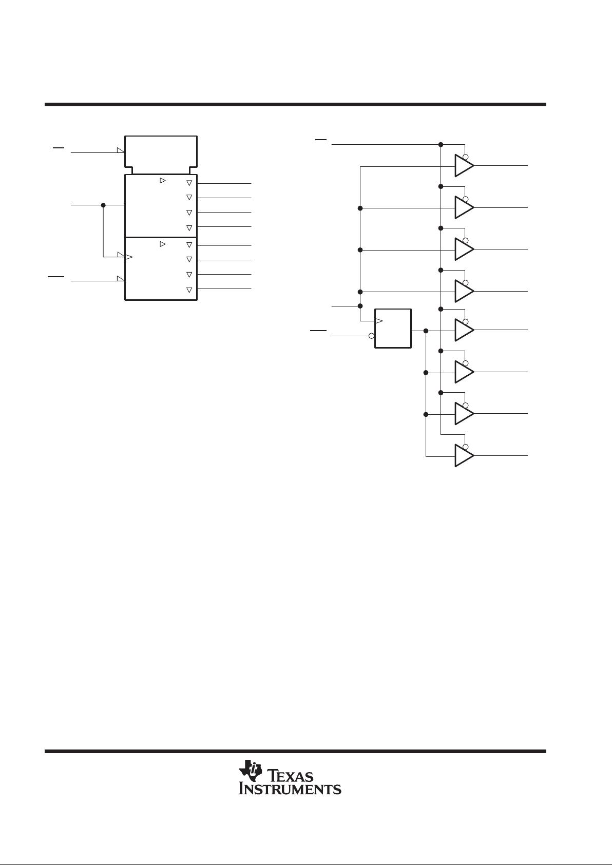
four Y outputs switch in phase and at the same frequency as the clock (CLK) input. The four Q outputs switch
at one-half the frequency of CLK.
When the output-enable (OE) input is low and the clear (CLR) input is high, the Y outputs follow CLK and the
Q outputs toggle on low-to-high transitions of CLK. T aking CLR low asynchronously resets the Q outputs to the
low level. When OE
is high, the outputs are in the high-impedance state.
The CDC339 is characterized for operation from –40°C to 85°C.
FUNCTION TABLE
INPUTS
OUTPUTS
OE CLR CLK Y1–Y4 Q1–Q4
H X X Z Z
L LL L L
L LH H L
L HL LQ
0
†
L H ↑ H Q
0
†
†
The level of the Q outputs before the
indicated steady-state input conditions were
established.
Copyright 1994, Texas Instruments Incorporated
PRODUCTION DATA information is current as of publication date.
Products conform to specifications per the terms of Texas Instruments
standard warranty. Production processing does not necessarily include
testing of all parameters.
EPIC-ΙΙB is a trademark of Texas Instruments Incorporated.
Please be aware that an important notice concerning availability, standard warranty, and use in critical applications of
Texas Instruments semiconductor products and disclaimers thereto appears at the end of this data sheet.
1
2
3
4
5
6
7
8
9
10
20
19
18
17
16
15
14
13
12
11
Y3
GND
Y4
V
CC
OE
CLR
V
CC
Q4
GND
Q3
Y2
GND
Y1
V
CC
CLK
GND
V
CC
Q1
GND
Q2
DB OR DW PACKAGE
(TOP VIEW)

CDC339
CLOCK DRIVER
WITH 3-STATE OUTPUTS
SCAS331 – DECEMBER 1992 – REVISED MARCH 1994
2
POST OFFICE BOX 655303 • DALLAS, TEXAS 75265
logic symbol
†
logic diagram (positive logic)
EN
5
16
CLK
R
6
T
Y1
18
Y2
20
Y3
1
Y4
3
T
Y1
18
Q1
13
Q2
11
Q3
10
Q4
8
OE
CLR
Y2
20
Y3
1
Y4
3
Q1
13
Q2
11
Q3
10
Q4
8
R
16
CLK
CLR
OE
5
6
†
This symbol is in accordance with ANSI/IEEE Std 91-1984
and IEC Publication 617-12.
absolute maximum ratings over operating free-air temperature range (unless otherwise noted)
‡
Supply voltage range, VCC –0.5 V to 7 V. . . . . . . . . . . . . . . . . . . . . . . . . . . . . . . . . . . . . . . . . . . . . . . . . . . . . . . . . .
Input voltage range, VI (see Note 1) –0.5 V to 7 V. . . . . . . . . . . . . . . . . . . . . . . . . . . . . . . . . . . . . . . . . . . . . . . . . .
Voltage range applied to any output in the disabled or power-off state, VO –0.5 V to 5.5 V. . . . . . . . . . . . . . .
Current into any output in the low state, IO 96 mA. . . . . . . . . . . . . . . . . . . . . . . . . . . . . . . . . . . . . . . . . . . . . . . . . .
Input clamp current, I
IK
(V
I
< 0) –18 mA. . . . . . . . . . . . . . . . . . . . . . . . . . . . . . . . . . . . . . . . . . . . . . . . . . . . . . . . . . .
Output clamp current, I
OK
(V
O
< 0) –50 mA. . . . . . . . . . . . . . . . . . . . . . . . . . . . . . . . . . . . . . . . . . . . . . . . . . . . . . .
Maximum power dissipation at TA = 55°C (in still air) (see Note 2):DB package 0.6 W. . . . . . . . . . . . . . . . . .
DW package 1.6 W. . . . . . . . . . . . . . . . .
Storage temperature range, T
stg
–65°C to 150°C. . . . . . . . . . . . . . . . . . . . . . . . . . . . . . . . . . . . . . . . . . . . . . . . . .
‡
Stresses beyond those listed under “absolute maximum ratings” may cause permanent damage to the device. These are stress ratings only, and
functional operation of the device at these or any other conditions beyond those indicated under “recommended operating conditions” is not
implied. Exposure to absolute-maximum-rated conditions for extended periods may affect device reliability.
NOTES: 1. The input and output negative-voltage ratings may be exceeded if the input and output clamp-current ratings are observed.
2. The maximum package power dissipation is calculated using a junction temperature of 150°C and a board trace length of 750 mils.
For more information, refer to the
Package Thermal Considerations
application note in the 1994
ABT Advanced BiCMOS T echnology
Data Book
, literature number SCBD002B.

CDC339
CLOCK DRIVER
WITH 3-STATE OUTPUTS
SCAS331 – DECEMBER 1992 – REVISED MARCH 1994
3
POST OFFICE BOX 655303 • DALLAS, TEXAS 75265
recommended operating conditions (see Note 3)
MIN MAX UNIT
V
CC
Supply voltage 4.75 5.25 V
V
IH
High-level input voltage 2 V
V
IL
Low-level input voltage 0.8 V
V
I
Input voltage 0 V
CC
V
I
OH
High-level output current –48 mA
I
OL
Low-level output current 48 mA
f
clock
Input clock frequency 80 MHz
T
A
Operating free-air temperature –40 85 °C
NOTE 3: Unused pins (input or I/O) must be held high or low.
electrical characteristics over recommended operating free-air temperature range (unless
otherwise noted)
PARAMETER TEST CONDITIONS MIN TYP†MAX UNIT
V
IK
VCC = 4.75 V , II = –18 mA –1.2 V
V
OH
VCC = 4.75 V , IOH = – 48 mA 2 V
V
OL
VCC = 4.75 V , IOL = 48 mA 0.5 V
I
IH
VCC = 5.25 V , VI = 2.7 V 50 µA
I
IL
VCC = 5.25 V , VI = 0.5 V –50 µA
I
OZ
VCC = 5.25 V , VO = 2.7 V or 0.5 V ±50 µA
I
O
‡
VCC = 5.25 V , VO = 2.5 V –50 –180 mA
Outputs high 70
I
CC
VCC = 5.25 V , IO = 0,
Outputs low 85
mA
V
I
=
V
CC
or
GND
Outputs disabled 70
C
i
VI = 2.5 V or 0.5 V 3 pF
C
o
VO = 2.5 V or 0.5 V 8 pF
†
All typical values are at VCC = 5 V, TA = 25°C.
‡
Not more than one output should be tested at a time, and the duration of the test should not exceed one second.
timing requirements over recommended ranges of supply voltage and operating free-air
temperature
MIN MAX UNIT
f
clock
Clock frequency 80 MHz
CLR low 4
t
w
Pulse duration
CLK low
4
ns
CLK high 4
t
su
Setup time CLR inactive before CLK↑ 2 ns
Clock duty cycle 40% 60%
 Loading...