

Page 1
查询CDC318供应商
CDC318
1-LINE TO 18-LINE CLOCK DRIVER
WITH I
SCAS587B – JANUARY 1997 – REVISED MARCH 1998
2
C CONTROL INTERFACE
D
High-Speed, Low-Skew 1-to-18 Clock Buffer
for Synchronous DRAM (SDRAM) Clock
Buffering Applications
D
Output Skew, t
D
Pulse Skew, t
D
Supports up to Four Unbuffered SDRAM
, Less Than 250 ps
sk(o)
, Less Than 650 ps
sk(p)
Dual Inline Memory Modules (DIMMs)
D
I2C Serial Interface Provides Individual
Enable Control for Each Output
D
Operates at 3.3 V
D
Distributed VCC and Ground Pins Reduce
Switching Noise
D
ESD Protection Exceeds 2000 V Per
MIL-STD-883, Method 3015
D
Packaged in 48-Pin Shrink Small Outline
(DL) Package
description
The CDC318 is a high-performance clock buffer
that distributes one input (A) to 18 outputs (Y) with
minimum skew for clock distribution. The CDC318
operates from a 3.3-V power supply, and is
characterized for operation from 0°C to 70°C.
The device provides a standard mode
(100K-bits/s) I2C serial interface for device
control. The implementation is as a slave/receiver.
The device address is specified in the I
address table. Both of the I2C inputs (SDA T A and
SCLOCK) provide integrated pullup resistors
(typically 140 kΩ) and are 5-V tolerant.
2
C device
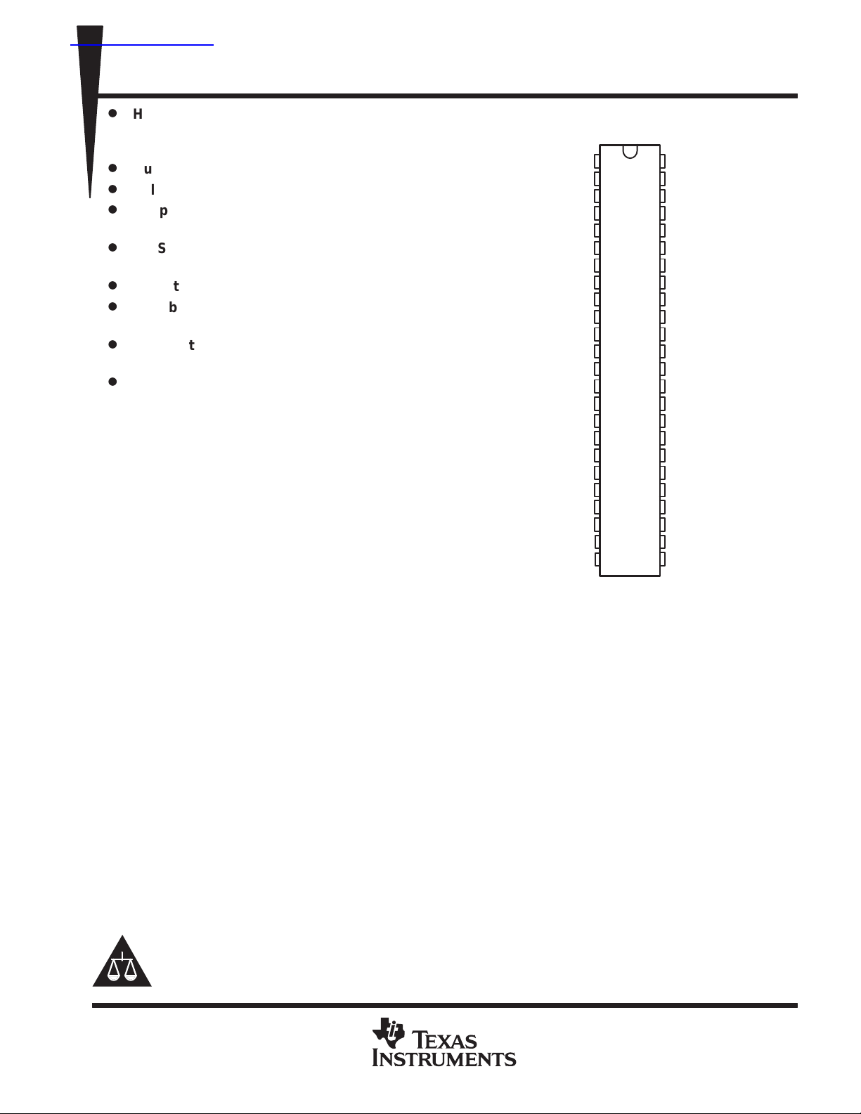
DL PACKAGE
(TOP VIEW)
1
2
3
4
5
6
7
8
9
10
11
12
13
14
15
16
17
18
19
20
21
22
23
24
48
47
46
45
44
43
42
41
40
39
38
37
36
35
34
33
32
31
30
29
28
27
26
25
NC
NC
V
CC
4Y3
4Y2
GND
V
CC
4Y1
4Y0
GND
OE
V
CC
3Y3
3Y2
GND
V
CC
3Y1
3Y0
GND
V
CC
5Y1
GND
GND
SCLOCK
NC
NC
V
CC
1Y0
1Y1
GND
V
CC
1Y2
1Y3
GND
A
V
CC
2Y0
2Y1
GND
V
CC
2Y2
2Y3
GND
V
CC
5Y0
GND
V
CC
SDATA
NC – No internal connection
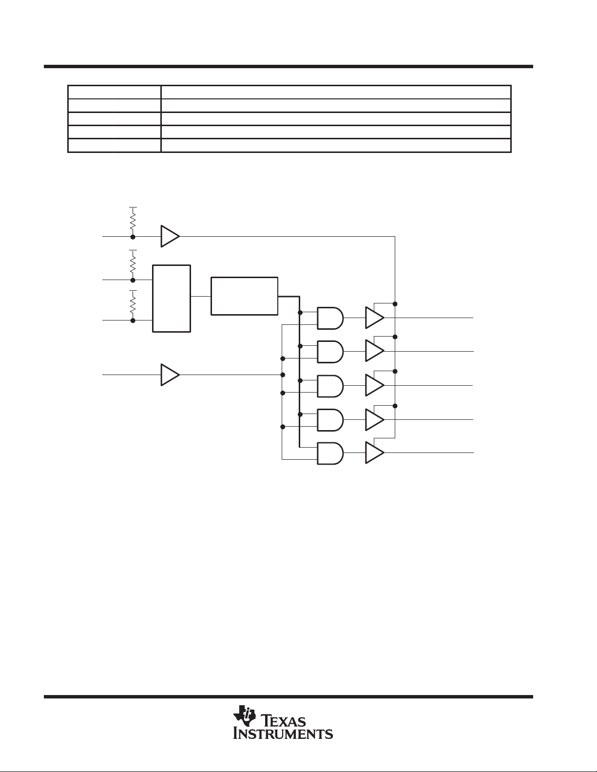
Three 8-bit I2C registers provide individual enable control for each of the outputs. All outputs default to enabled
at powerup. Each output can be placed in a disabled mode with a low-level output when a low-level control bit
is written to the control register. The registers are write only and must be accessed in sequential order (i.e.,
random access of the registers is not supported).
The CDC318 provides 3-state outputs for testing and debugging purposes. The outputs can be placed in a
high-impedance state via the output-enable (OE) input. When OE is high, all outputs are in the operational state.
When OE is low, the outputs are placed in a high-impedance state. OE provides an integrated pullup resistor.
Please be aware that an important notice concerning availability, standard warranty, and use in critical applications of
Texas Instruments semiconductor products and disclaimers thereto appears at the end of this data sheet.
Intel is a trademark of Intel Corporation
PRODUCTION DATA information is current as of publication date.
Products conform to specifications per the terms of Texas Instruments
standard warranty. Production processing does not necessarily include
testing of all parameters.
POST OFFICE BOX 655303 • DALLAS, TEXAS 75265
Copyright 1998, Texas Instruments Incorporated
1
Page 2
CDC318
1-LINE TO 18-LINE CLOCK DRIVER
WITH I
SCAS587B – JANUARY 1997 – REVISED MARCH 1998
logic diagram (positive logic)
2
C CONTROL INTERFACE
INPUTS
OE A 1Y0–1Y3 2Y0–2Y3 3Y0–3Y3 4Y0–4Y3 5Y0–5Y1
L X Hi-Z Hi-Z Hi-Z Hi-Z Hi-Z
H L L L L L L
H H H
†
The function table assumes that all outputs are enabled via the appropriate I2C configuration register bit. If the output is disabled
via the appropriate configuration bit, then the output is driven to a low state, regardless of the state of the A input.
38
OE
†
FUNCTION TABLE
†
H
OUTPUTS
†
H
†
H
†
H
SDATA
SCLOCK
24
I2C
I2C
25
11
A
Register
Space
18
/
4, 5, 8, 9
13, 14, 17, 18
31, 32, 35, 36
40, 41, 44, 45
21, 28
1Y0–1Y3
2Y0–2Y3
3Y0–3Y3
4Y0–4Y3
5Y0–5Y1
2
POST OFFICE BOX 655303 • DALLAS, TEXAS 75265
Page 3
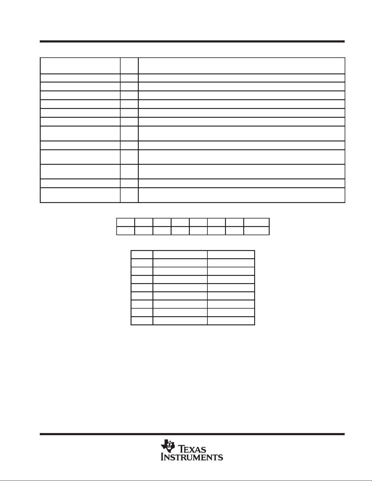
I/O
DESCRIPTION
Terminal Functions
TERMINAL
NAME NO.
1Y0–1Y3 4, 5, 8, 9 O 3.3-V SDRAM byte 0 clock outputs
2Y0–2Y3
3Y0–3Y3
4Y0–4Y3
5Y0–5Y1
A
OE
SCLOCK
SDATA
GND
NC
V
CC
13, 14, 17, 18 O 3.3-V SDRAM byte 1 clock outputs
31, 32, 35, 36 O 3.3-V SDRAM byte 2 clock outputs
40, 41, 44, 45 O 3.3-V SDRAM byte 3 clock outputs
21, 28 O 3.3-V clock outputs provided for feedback control of external phase-locked loops (PLLs)
11 I Clock input
38 I
25 I I2C serial clock input. A nominal 140-kΩ pullup resistor is internally integrated.
24 I/O
6, 10, 15, 19, 22, 26,
27, 30, 34, 39, 43
1, 2, 47, 48 No internal connection. Reserved for future use.
3, 7, 12, 16, 20, 23,
29, 33, 37, 42, 46
Output enable. When asserted, OE puts all outputs in a high-impedance state. A nominal
140-kΩ pullup resistor is internally integrated.
Bidirectional I2C serial data input/output. A nominal 140-kΩ pullup resistor is internally
integrated.
Ground
3.3-V power supply
CDC318
1-LINE TO 18-LINE CLOCK DRIVER
WITH I
SCAS587B – JANUARY 1997 – REVISED MARCH 1998
2
C CONTROL INTERFACE
I2C DEVICE ADDRESS
A7
A6 A5 A4 A3 A2 A1 A0 (R/W)
H H L H L L H —
I2C BYTE 0-BIT DEFINITION
BIT
7 2Y3 enable (pin 18) H
6 2Y2 enable (pin 17) H
5 2Y1 enable (pin 14) H
4 2Y0 enable (pin 13) H
3 1Y3 enable (pin 9) H
2 1Y2 enable (pin 8) H
1 1Y1 enable (pin 5) H
0 1Y0 enable (pin 4) H
†
When the value of the bit is high, the output is enabled.
When the value of the bit is low, the output is forced to a
low state. The default value of all bits is high.
DEFINITION DEFAULT VALUE
†
POST OFFICE BOX 655303 • DALLAS, TEXAS 75265
3
Page 4
CDC318
1-LINE TO 18-LINE CLOCK DRIVER
WITH I
SCAS587B – JANUARY 1997 – REVISED MARCH 1998
2
C CONTROL INTERFACE
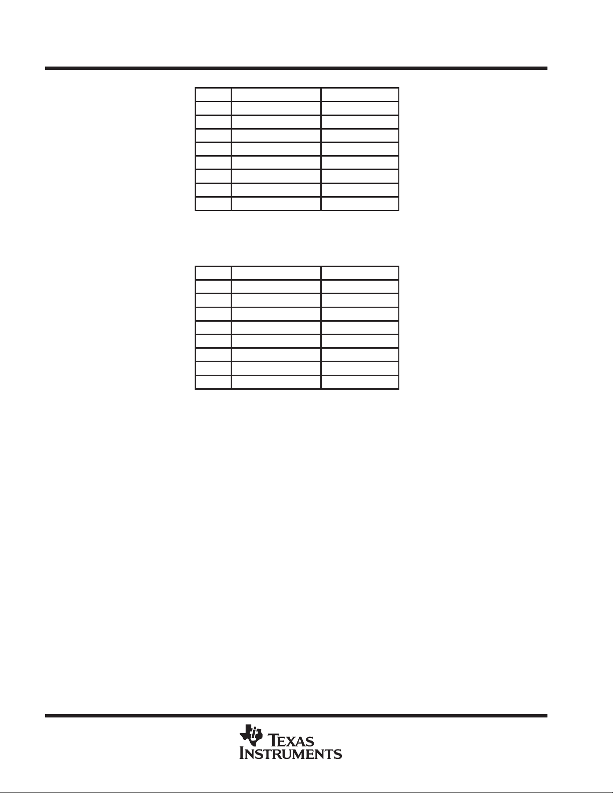
I2C BYTE 1-BIT DEFINITION
BIT
7 4Y3 enable (pin 45) H
6 4Y2 enable (pin 44) H
5 4Y1 enable (pin 41) H
4 4Y0 enable (pin 40) H
3 3Y3 enable (pin 36) H
2 3Y2 enable (pin 35) H
1 3Y1 enable (pin 32) H
0 3Y0 enable (pin 31) H
†
When the value of the bit is high, the output is enabled.
When the value of the bit is low, the output is forced to a
low state. The default value of all bits is high.
BIT
7 5Y1 enable (pin 28) H
6 5Y0 enable (pin 21) H
5 Reserved H
4 Reserved H
3 Reserved H
2 Reserved H
1 Reserved H
0 Reserved H
†
When the value of the bit is high, the output is enabled.
When the value of the bit is low, the output is forced to a
low state. The default value of all bits is high.
DEFINITION DEFAULT VALUE
I2C BYTE 2-BIT DEFINITION
DEFINITION DEFAULT VALUE
†
†
4
POST OFFICE BOX 655303 • DALLAS, TEXAS 75265
Page 5
CDC318
1-LINE TO 18-LINE CLOCK DRIVER
WITH I
SCAS587B – JANUARY 1997 – REVISED MARCH 1998
2
C CONTROL INTERFACE
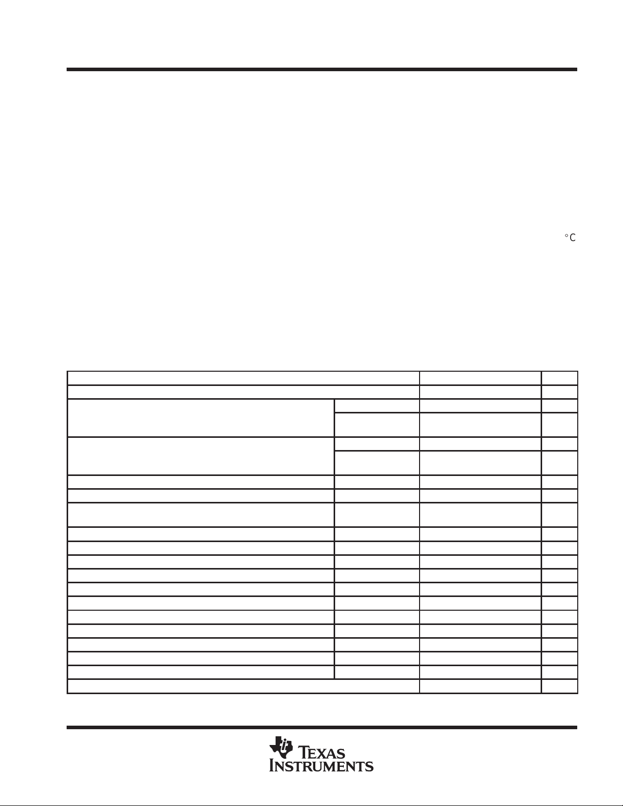
absolute maximum ratings over operating free-air temperature range (unless otherwise noted)
Supply voltage range, V
Input voltage range, V
Input voltage range, V
Output voltage range, V
Voltage range applied to any output in the high or power-off state, VO –0.5 V to VCC +0.5 V. . . . . . . . . . . . .
Current into any output in the low state (except SDATA), I
Current into SDATA in the low state, IO 12 mA. . . . . . . . . . . . . . . . . . . . . . . . . . . . . . . . . . . . . . . . . . . . . . . . . . . . .
Input clamp current, IIK (VI < 0) (SCLOCK) –50 mA. . . . . . . . . . . . . . . . . . . . . . . . . . . . . . . . . . . . . . . . . . . . . . . . .
Output clamp current, IOK (VO < 0) (SDATA) –50 mA. . . . . . . . . . . . . . . . . . . . . . . . . . . . . . . . . . . . . . . . . . . . . . .
Package thermal impedance, θ
Storage temperature range, T
Lead temperature 1,6 mm (1/16 inch) from case for 10 seconds 260_C. . . . . . . . . . . . . . . . . . . . . . . . . . . . . . . .
†
Stresses beyond those listed under “absolute maximum ratings” may cause permanent damage to the device. These are stress ratings only, and
functional operation of the device at these or any other conditions beyond those indicated under “recommended operating conditions” is not
implied. Exposure to absolute-maximum-rated conditions for extended periods may affect device reliability.
NOTES: 1. The input and output negative-voltage ratings may be exceeded if the input and output clamp-current ratings are observed.
2. The package thermal impedance is calculated in accordance with EIA/JEDEC Std JESD51, except for through-hole packages,
which use a trace length of zero. The absolute maximum power dissipation allowed at TA = 55°C (in still air) is 1.2 W.
3. Thermal impedance (ΘJA) can be considerably lower if the device is soldered on the PCB board with a copper layer underneath the
package. A simulation on a PCB board (3 in. × 3 in.) with two internal copper planes (1 oz. cu, 0.036 mm thick) and 0.071 mm cu
(202) in area underneath the package, resulted in ΘJA = 60°C/W. This would allow 1.2 W total power dissipation at TA = 70°C.
–0.5 V to 4.6 V. . . . . . . . . . . . . . . . . . . . . . . . . . . . . . . . . . . . . . . . . . . . . . . . . . . . . . . . .
CC
(see Note 1) –0.5 V to 4.6 V. . . . . . . . . . . . . . . . . . . . . . . . . . . . . . . . . . . . . . . . . . . . . . . . .
I
(SCLOCK, SDATA) (see Note 1) –0.5 V to 6.5 V. . . . . . . . . . . . . . . . . . . . . . . . . . . . . . .
I
(SDATA) (see Note 1) –0.5 V to 6.5 V. . . . . . . . . . . . . . . . . . . . . . . . . . . . . . . . . . . . . .
O
48 mA. . . . . . . . . . . . . . . . . . . . . . . . . . . . . . . . . . . .
O
(see Notes 2 and 3) 84°C/W. . . . . . . . . . . . . . . . . . . . . . . . . . . . . . . . . . . . . . .
JA
–65°C to 150°C. . . . . . . . . . . . . . . . . . . . . . . . . . . . . . . . . . . . . . . . . . . . . . . . . . .
stg
recommended operating conditions (see Note 4)
MIN TYP MAX UNIT
V
CC
V
IH
V
IL
I
OH
I
OL
r
i
f
(SCL)
t
(BUS)
t
su(START)
t
h(START)
t
w(SCLL)
t
w(SCLH)
t
r(SDATA)
t
f(SDATA)
t
su(SDATA)
t
h(SDATA)
t
su(STOP)
T
A
NOTE 4: The CMOS-level inputs fall within these limits: VIH min = 0.7 × VCC and VIL max = 0.3 × VCC.
3.3-V core supply voltage 3.135 3.465 V
A, OE 2 VCC+0.3 V
High-level input voltage
Low-level input voltage
High-level output current Y outputs 1 mA
Low-level output current Y outputs –1 mA
Input resistance to V
SCLOCK frequency 100 kHz
Bus free time 4.7 µs
STAR T setup time 4.7 µs
STAR T hold time 4 µs
SCLOCK low pulse duration 4.7 µs
SCLOCK high pulse duration 4 µs
SDATA input rise time 1000 ns
SDATA input fall time 300 ns
SDATA setup time 250 ns
SDATA hold time 0 ns
STOP setup time 4 µs
Operating free-air temperature 0 70 °C
CC
SDATA, SCLOCK
(see Note 3)
A, OE –0.3 0.8 V
SDATA, SCLOCK
(see Note 3)
SDATA, SCLOCK
(see Note 3)
2.2 5.5 V
0 1.04 V
140 kΩ
†
POST OFFICE BOX 655303 • DALLAS, TEXAS 75265
5
Page 6

CDC318
SDATA
V
135 V
IOHHigh-level output current
1-LINE TO 18-LINE CLOCK DRIVER
WITH I
SCAS587B – JANUARY 1997 – REVISED MARCH 1998
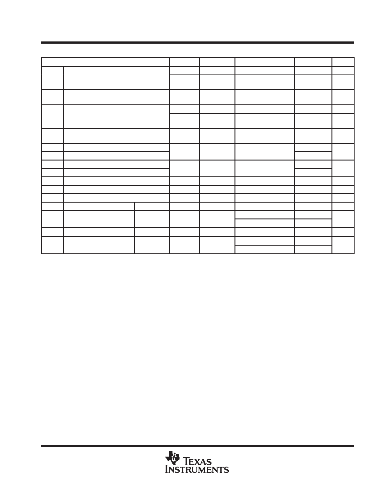
electrical characteristics over recommended operating free-air temperature range (unless
otherwise noted)
V
V
V
I
I
I
I
I
I
∆I
C
C
C
2
C CONTROL INTERFACE
PARAMETER TEST CONDITIONS MIN TYP MAX UNIT
Input clamp voltage VCC = 3.135 V, II = –18 mA –1.2 V
IK
High-level output voltage Y outputs VCC = 3.135 V, IOH = –1 mA 2.4 V
OH
Y outputs VCC = 3.135 V, IOL = 1 mA 0.4
Low-level output voltage
OL
SDATA VCC = 3.135 V, VO = VCC MAX 20 µA
p
Low-level output current Y outputs
OL
High-level input current
IH
Low-level input current
IL
High-impedance-state output current VCC = 3.465 V, VO = 3.465 V or 0 ±10 µA
OZ
Off-state current SCLOCK, SDATA VCC = 0, VI = 0 V to 5.5 V 50 µA
off
Supply current VCC = 3.465 V, IO = 0 0.2 0.5 mA
CC
Change in supply current
CC
Dyanmic ICC at 100 MHz VCC = 3.465 V, CL = 20 pF, 360 mA
Input capacitiance VI = VCC or GND, VCC = 3.3 V 4 pF
I
Output capacitance VO = VCC or GND, VCC = 3.3 V 6 pF
O
SDATA I/O capacitance V
I/O
Y outputs
A 5
OE
SCLOCK, SDATA 20
A –5
OE
SCLOCK, SDATA –10 –50
= 3.
CC
VCC = 3.135 V, VO = 2 V –54 –126
VCC = 3.3 V, VO = 2.6 V –54
VCC = 3.465 V, VO = 3.135 V –21 –46
VCC = 3.135 V, VO = 1 V 49 118
VCC = 3.3 V, VO = 0.7 V 58
VCC = 3.465 V, VO = 0.4 V 23 53
VCC = 3.465 V, VI = V
VCC = 3.465 V, VI = GND
VCC = 3.135 V to 3.465 V,
One input at VCC – 0.6 V,
All other inputs at VCC or GND
= VCC or GND, VCC = 3.3 V 7 pF
I/O
IOL = 3 mA 0.4
IOL = 6 mA 0.6
CC
–10
mA
mA
20
–50
500 µA
V
µA
µA
6
POST OFFICE BOX 655303 • DALLAS, TEXAS 75265
Page 7
OE
Y
ns
OE
Y
ns
t
(
SDATA
ns
t
(
SDATA
ns
1-LINE TO 18-LINE CLOCK DRIVER
WITH I
SCAS587B – JANUARY 1997 – REVISED MARCH 1998
switching characteristics over recommended operating conditions
PARAMETER FROM TO TEST CONDITIONS MIN MAX UNIT
A Y 1.2 4.5 ns
t
PLH
t
PLH
t
PHL
t
PHL
t
PZH
t
PZL
t
PHZ
t
PLZ
t
sk(o)
t
sk(p)
t
sk(pr)
t
r
r
t
f
f
NOTE 5: This parameter has a lower limit than BUS specification. This allows use of series resistors for current spike protectio n.
Low-to-high level propagation delay time
Low-to-high level propagation delay time SDATA↑ Y
High-to-low level propagation delay time
High-to-low level propagation delay time SDATA↑ Y
Enable time to the high level
Enable time to the low level
Disable time from the high level
Disable time from the low level
Skew time A Y 250 ps
Skew time A Y 650 ps
Skew time A Y 1 ns
Rise time Y 0.5 2.4 ns
Rise time (see Note 5 and
Figure 3)
Fall time Y 0.5 2.3 ns
Fall time (see Note 5 and
Figure 3)
SCLOCK↓
A Y 1.2 4.5 ns
SCLOCK↓
SDATA
valid
SDATA
valid
VCC = 3.3 V ±0.185 V ,
See Figure 3
VCC = 3.3 V ±0.185 V ,
See Figure 3
VCC = 3.3 V ±0.185 V ,
See Figure 3
VCC = 3.3 V ±0.185 V ,
See Figure 3
CL = 10 pF 6
CL = 400 pF 950
CL = 10 pF 20
CL = 400 pF 250
2
C CONTROL INTERFACE
1 7
1 7
1 7
1 7
CDC318
2 µs
150 ns
2 µs
150 ns
POST OFFICE BOX 655303 • DALLAS, TEXAS 75265
7
Page 8

CDC318
1-LINE TO 18-LINE CLOCK DRIVER
WITH I
SCAS587B – JANUARY 1997 – REVISED MARCH 1998
2
C CONTROL INTERFACE
PARAMETER MEASUREMENT INFORMATION
From Output
Under Test
CL = 30 pF
(see Note A)
LOAD CIRCUIT FOR tpd AND t
From Output
Under Test
(see Note A)
500 Ω
CL = 30 pF
500 Ω
sk
S1
6 V
GND
Open
Input
TEST
t
PLH/tPHL
t
PLZ/tPZL
t
PHZ/tPZH
t
w
1.5 V 1.5 V
VOLTAGE WAVEFORMS
S1
Open
6 V
GND
3 V
0 V
LOAD CIRCUIT FOR tr AND t
Input
t
PLH
Output
NOTES: A. CL includes probe and jig capacitance.
B. Waveform 1 is for an output with internal conditions such that the output is low except when disabled by the output control.
C. All input pulses are supplied by generators having the following characteristics: PRR ≤ 10 MHz, ZO = 50 Ω, tr ≤ 2.5 ns, tf≤ 2.5 ns.
D. The outputs are measured one at a time with one transition per measurement.
1.5 V 1.5 V
2.4 V
0.4 V
t
r
VOLTAGE WAVEFORMS
Waveform 2 is for an output with internal conditions such that the output is high except when disabled by the output control.
1.5 V
2.4 V
t
f
Figure 1. Load Circuit and Voltage Waveforms
f
t
PHL
0.4 V
3 V
0 V
V
V
OH
OL
Output
Enable
(high-level
enabling)
Output
Waveform 1
S1 at 6 V
(see Note B)
Output
Waveform 2
S1 at GND
(see Note B)
t
PZL
t
PZH
VOLTAGE WAVEFORMS
t
PLZ
1.5 V
t
PHZ
1.5 V
1.5 V1.5 V
VOL + 0.3 V
VOH – 0.3 V
V
CC
0 V
≈ 3 V
V
OL
V
OH
≈ 0 V
8
POST OFFICE BOX 655303 • DALLAS, TEXAS 75265
Page 9

CDC318
1-LINE TO 18-LINE CLOCK DRIVER
WITH I
SCAS587B – JANUARY 1997 – REVISED MARCH 1998
PARAMETER MEASUREMENT INFORMATION
A
1Y0
t
PHL1
1Y1
t
PHL2
1Y2
t
PHL3
1Y3
t
PHL4
2Y0
t
PHL5
2Y1
t
PHL6
2Y2
t
PHL7
2Y3
t
PHL8
3Y0
t
PHL9
3Y1
t
PHL10
3Y2
t
PHL11
3Y3
t
PHL12
4Y0
t
PHL13
4Y1
t
PHL14
4Y2
t
PHL15
4Y3
t
PHL16
5Y0
t
PHL17
5Y1
t
PHL18
t
PLH1
t
PLH2
t
PLH3
t
PLH4
t
PLH5
t
PLH6
t
PLH7
t
PLH8
t
PLH9
t
PLH10
t
PLH11
t
PLH12
t
PLH13
t
PLH14
t
PLH15
t
PLH16
t
PLH17
t
PLH18
2
C CONTROL INTERFACE
NOTES: A. Output skew, t
– The difference between the fastest and slowest of t
– The difference between the fastest and slowest of t
B. Pulse skew, t
C. Process skew, t
– The difference between the fastest and slowest of t
– The difference between the fastest and slowest of t
, is calculated as the greater of:
sk(o)
, is calculated as the greater of |t
sk(p)
, is calculated as the greater of:
sk(pr)
PLHn
(n = 1:18)
PLHn
(n = 1:18)
PHLn
– t
PHLn
(n = 1:18) across multiple devices under identical operating conditions
PLHn
(n = 1:18) across multiple devices under identical operating conditions
PHLn
Figure 2. Waveforms for Calculation of t
POST OFFICE BOX 655303 • DALLAS, TEXAS 75265
| (n = 1:18)
sk(o)
, t
sk(p)
, t
sk(pr)
9
Page 10

CDC318
1-LINE TO 18-LINE CLOCK DRIVER
WITH I
SCAS587B – JANUARY 1997 – REVISED MARCH 1998
2
C CONTROL INTERFACE
PARAMETER MEASUREMENT INFORMATION
CL = 10 pF or
CL = 400 pF
VO = 3.3 V
RL = 1 kΩ
DUT
GND
TEST CIRCUIT
SCLOCK
t
SDATA
t
su(START)
(BUS)
t
f(SDATA)
t
h(START)
Start or
Repeat Start
Condition
Start
Condition
(S)
t
w(SCLL)
t
r
Bit 7
MSB
t
f
t
r(SDATA)
t
su(SDATA)
BYTE DESCRIPTION
1 I2C address
2 Command (dummy value, ignored)
3 Byte count (dummy value, ignored)
4 I2C data byte 0
5 I2C data byte 1
6 I2C data byte 2
NOTES: A. The repeat start condition is not supported.
B. All input pulses are supplied by generators having hte following characteristics: PRR ≤ 100 kHz, ZO = 50 Ω, tr ≥ 10 ns, tf ≥ 10 ns.
4 to 6 Bytes for Complete Device
t
w(SCLH)
Bit 6
Programming
t
h(SDATA)
VOLTAGE WAVEFORMS
Bit 0
LSB
(R/W)
t
PHL
Repeat Start
(see Note A)
Acknowledge
Condition
(A)
t
PLH
Condition
t
su(START)
t
su(STOP)
Stop Condition
Stop
(P)
0.7 V
0.3 V
0.7 V
0.3 V
CC
CC
CC
CC
10
Figure 3. Propagation Delay Times, t
POST OFFICE BOX 655303 • DALLAS, TEXAS 75265
and t
r
f
Page 11

CDC318
1-LINE TO 18-LINE CLOCK DRIVER
WITH I
SCAS587B – JANUARY 1997 – REVISED MARCH 1998
MECHANICAL INFORMATION
DL (R-PDSO-G**) PLASTIC SMALL-OUTLINE PACKAGE
48 PIN SHOWN
0.025 (0,635)
0.012 (0,305)
0.008 (0,203)
48
0.005 (0,13)
25
0.299 (7,59)
0.291 (7,39)
M
0.006 (0,15) NOM
0.420 (10,67)
0.395 (10,03)
2
C CONTROL INTERFACE
Gage Plane
0.010 (0,25)
1
A
0.110 (2,79) MAX
NOTES: A. All linear dimensions are in inches (millimeters).
B. This drawing is subject to change without notice.
C. Body dimensions do not include mold flash or protrusion not to exceed 0.006 (0,15).
D. Falls within JEDEC MO-118
0.008 (0,20) MIN
DIM
A MAX
A MIN
24
PINS **
0.380
(9,65)
0.370
(9,40)
Seating Plane
0.004 (0,10)
4828
0.630
(16,00)
0.620
(15,75)
0°–8°
0.040 (1,02)
0.020 (0,51)
56
0.730
(18,54)
0.720
(18,29)
4040048/C 03/97
POST OFFICE BOX 655303 • DALLAS, TEXAS 75265
11
Page 12

IMPORTANT NOTICE
T exas Instruments and its subsidiaries (TI) reserve the right to make changes to their products or to discontinue
any product or service without notice, and advise customers to obtain the latest version of relevant information
to verify, before placing orders, that information being relied on is current and complete. All products are sold
subject to the terms and conditions of sale supplied at the time of order acknowledgement, including those
pertaining to warranty, patent infringement, and limitation of liability.
TI warrants performance of its semiconductor products to the specifications applicable at the time of sale in
accordance with TI’s standard warranty. Testing and other quality control techniques are utilized to the extent
TI deems necessary to support this warranty . Specific testing of all parameters of each device is not necessarily
performed, except those mandated by government requirements.
CERTAIN APPLICATIONS USING SEMICONDUCTOR PRODUCTS MAY INVOLVE POTENTIAL RISKS OF
DEATH, PERSONAL INJURY, OR SEVERE PROPERTY OR ENVIRONMENTAL DAMAGE (“CRITICAL
APPLICATIONS”). TI SEMICONDUCTOR PRODUCTS ARE NOT DESIGNED, AUTHORIZED, OR
WARRANTED TO BE SUITABLE FOR USE IN LIFE-SUPPORT DEVICES OR SYSTEMS OR OTHER
CRITICAL APPLICA TIONS. INCLUSION OF TI PRODUCTS IN SUCH APPLICATIONS IS UNDERST OOD TO
BE FULLY AT THE CUSTOMER’S RISK.
In order to minimize risks associated with the customer’s applications, adequate design and operating
safeguards must be provided by the customer to minimize inherent or procedural hazards.
TI assumes no liability for applications assistance or customer product design. TI does not warrant or represent
that any license, either express or implied, is granted under any patent right, copyright, mask work right, or other
intellectual property right of TI covering or relating to any combination, machine, or process in which such
semiconductor products or services might be or are used. TI’s publication of information regarding any third
party’s products or services does not constitute TI’s approval, warranty or endorsement thereof.
Copyright 1998, Texas Instruments Incorporated
 Loading...