

Page 1
查询CDC305供应商
CDC305
OCTAL DIVIDE-BY-2 CIRCUIT/CLOCK DRIVER
SCAS326A – JUNE 1990 – REVISED NOVEMBER 1995
D
Replaces SN74AS305
D
Maximum Output Skew of 1 ns
D
Maximum Pulse Skew of 1ns
D
TTL-Compatible Inputs and Outputs
D
Center-Pin VCC and GND Configurations
Minimize High-Speed Switching Noise
D
Package Options Include Plastic
Small-Outline (D) Package and Standard
Plastic (N) 300-mil DIPs
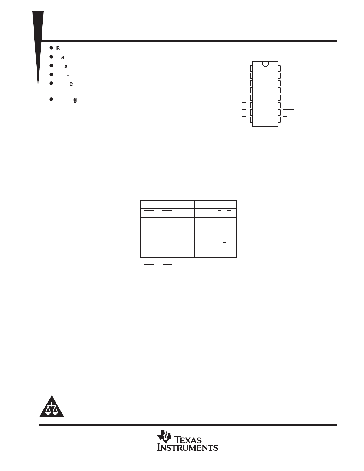
D OR N PACKAGE
(TOP VIEW)
1
Q3
2
Q4
GND
GND
GND
3
4
5
6
Q
5
7
6
Q
8
Q
7
16
15
14
13
12
11
10
Q2
Q1
CLR
V
CC
V
CC
CLK
PRE
Q8
9
description
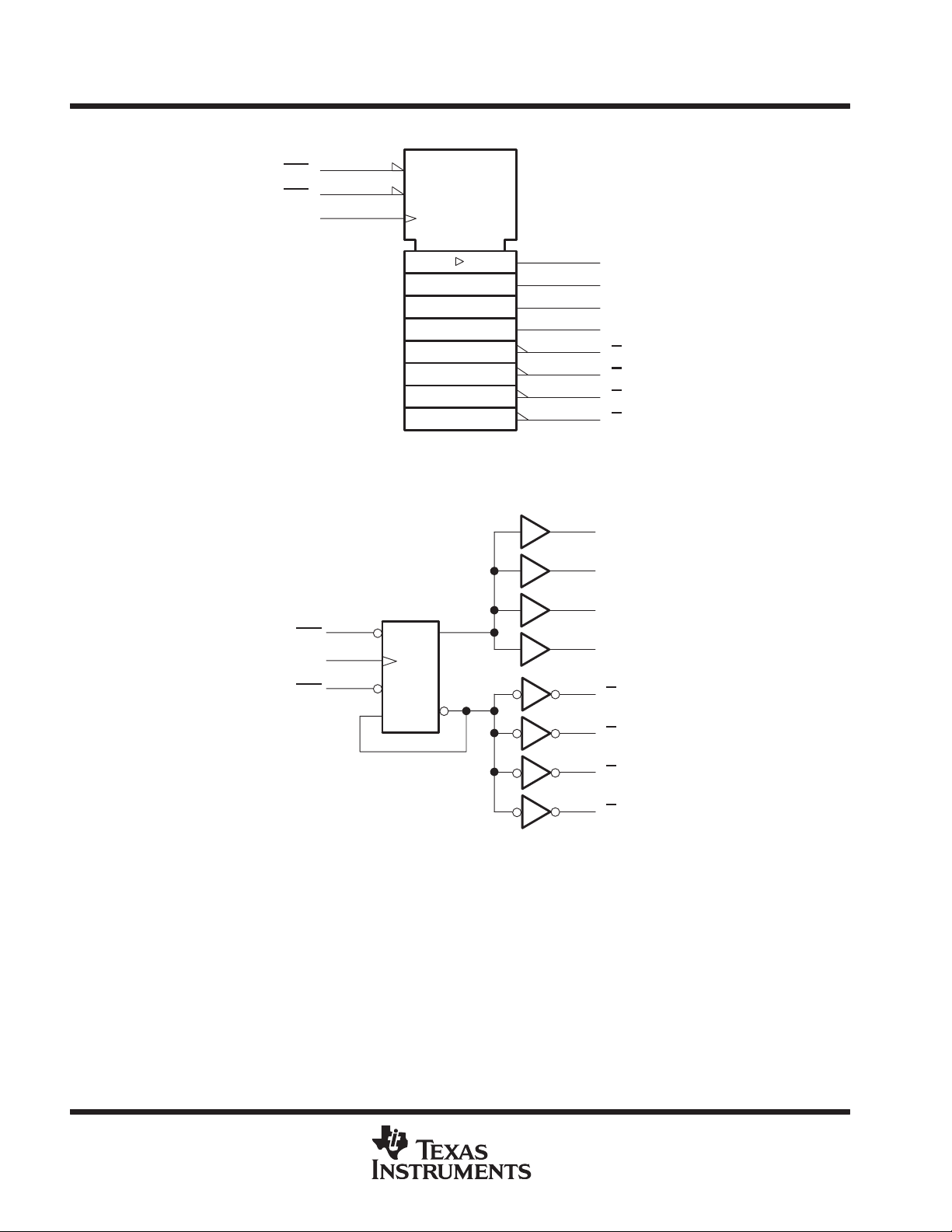
The CDC305 contains eight flip-flops designed to have low skew between outputs. The eight outputs (four
in-phase with CLK and four out-of-phase) toggle on successive CLK pulses. Preset (PRE) and clear (CLR)
inputs are provided to set the Q and Q outputs high or low independent of the clock (CLK) input.
The CDC305 has output and pulse-skew parameters t
when a divide-by-two function is required.
The CDC305 is characterized for operation from 0°C to 70°C.
FUNCTION TABLE
INPUTS
CLR PRE CLK Q1–Q4 Q5–Q8
L H X L H
H LX H L
L LXL†L
H HLQ0Q
H H ↑ Q
†
This configuration does not persist when
PRE
or CLR returns to its inactive (high)
level.
sk(o)
and t
sk(p)
OUTPUTS
0
to ensure performance as a clock driver
†
0
Q
0
Please be aware that an important notice concerning availability, standard warranty, and use in critical applications of
Texas Instruments semiconductor products and disclaimers thereto appears at the end of this data sheet.
PRODUCTION DATA information is current as of publication date.
Products conform to specifications per the terms of Texas Instruments
standard warranty. Production processing does not necessarily include
testing of all parameters.
POST OFFICE BOX 655303 • DALLAS, TEXAS 75265
Copyright 1995, Texas Instruments Incorporated
1
Page 2
CDC305
OCTAL DIVIDE-BY-2 CIRCUIT/CLOCK DRIVER
SCAS326A – JUNE 1990 – REVISED NOVEMBER 1995
logic symbol
†
This symbol is in accordance with ANSI/IEEE Std 91-1984 and IEC Publication 617-12.
†
CLR
PRE
CLK
14
10
11
S
R
C1
logic diagram (positive logic)
15
16
15
16
Q1
Q2
1
Q3
2
Q4
6
Q5
7
Q6
8
Q7
9
Q8
Q1
Q2
1
10
PRE
CLK
CLR
11
14
S
C1
R
1D
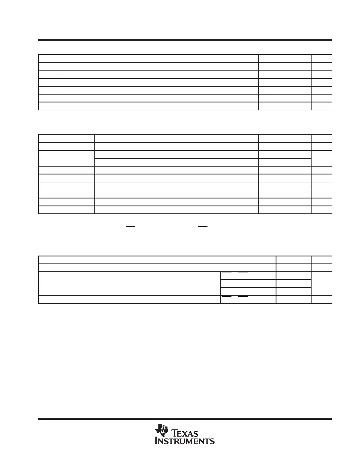
absolute maximum ratings over operating free-air temperature range (unless otherwise noted)
Supply voltage, V
Input voltage, V
7 V. . . . . . . . . . . . . . . . . . . . . . . . . . . . . . . . . . . . . . . . . . . . . . . . . . . . . . . . . . . . . . . . . . . . . . .
CC
7 V. . . . . . . . . . . . . . . . . . . . . . . . . . . . . . . . . . . . . . . . . . . . . . . . . . . . . . . . . . . . . . . . . . . . . . . . . . .
I
Q3
2
Q4
6
5
Q
7
Q6
8
Q7
9
Q8
‡
Maximum power dissipation at TA = 55°C (in still air) (see Note 1):D package 0.77 W. . . . . . . . . . . . . . . . . .
N package 1.2 W. . . . . . . . . . . . . . . . . . .
Storage temperature range, T
‡
Stresses beyond those listed under “absolute maximum ratings” may cause permanent damage to the device. These are stress ratings only and
functional operation of the device at these or any other conditions beyond those indicated under “recommended operating conditions” is not
implied. Exposure to absolute-maximum-rated conditions for extended periods may affect device reliability.
NOTE 1: The maximum package power dissipation is calculated using a junction temperature of 150°C and a board trace length of 300 mils,
except for the N package, which has a trace length of zero. For more information, refer to the
application note in the 1994
–65°C to 150°C. . . . . . . . . . . . . . . . . . . . . . . . . . . . . . . . . . . . . . . . . . . . . . . . . .
stg
ABT Advanced BiCMOS Technology Data Book
, literature number SCBD002B.
Package Thermal Considerations
2
POST OFFICE BOX 655303 • DALLAS, TEXAS 75265
Page 3
V
V
CDC305
OCTAL DIVIDE-BY-2 CIRCUIT/CLOCK DRIVER
SCAS326A – JUNE 1990 – REVISED NOVEMBER 1995
recommended operating conditions
MIN NOM MAX UNIT
V
CC
V
IH
V
IL
I
OH
I
OL
T
A
electrical characteristics over recommended operating free-air temperature range (unless
otherwise noted)
†
All typical values are at VCC = 5 V, TA = 25°C.
‡
The output conditions have been chosen to produce a current that closely approximates one half of the true short-circuit output current, IOS.
NOTE 2: ICC is measured with CLK and PRE
Supply voltage 4.5 5 5.5 V
High-level input voltage 2 V
Low-level input voltage 0.8 V
High-level output current –24 mA
Low-level output current 48 mA
Operating free-air temperature 0 70 °C
PARAMETER TEST CONDITIONS MIN TYP†MAX UNIT
V
V
I
I
I
I
I
IK
OH
OL
I
IH
IL
O
CC
‡
VCC = 4.5 V, II = –18 mA –1.2 V
VCC = 4.5 V to 5.5 V, IOH = –2 mA VCC–2
VCC = 4.5 V, IOH = –24 mA 2 2.8
VCC = 4.5 V, IOL = 48 mA 0.3 0.5 V
VCC = 5.5 V, VI = 7 V 0.1 mA
VCC = 5.5 V, VI = 2.7 V 20 µA
VCC = 5.5 V, VI = 0.4 V –0.5 mA
VCC = 5.5 V, VO = 2.25 V –50 –150 mA
VCC = 5.5 V, See Note 2 40 70 mA
grounded, then with CLK and CLR grounded.
timing requirements over recommended ranges of supply voltage and operating free-air
temperature
MIN MAX UNIT
f
clock
t
w
t
su
Clock frequency 0 80 MHz
CLR or PRE low 5
Pulse duration
Setup time before CLK↑ CLR or PRE inactive 6 ns
CLK high
CLK low 6
4
ns
POST OFFICE BOX 655303 • DALLAS, TEXAS 75265
3
Page 4
CDC305
CLK
Q, Q
R
500 Ω
C
pF
ns
PRE
CLR
Q, Q
R
500 Ω
C
50 pF
ns
()
See Figure 2
t
CLK
R
500 Ω
C
pF
ns
OCTAL DIVIDE-BY-2 CIRCUIT/CLOCK DRIVER
SCAS326A – JUNE 1990 – REVISED NOVEMBER 1995
switching characteristics over recommended ranges of supply voltage and operating free-air
temperature (unless otherwise noted) (see Figure 1)
PARAMETER
‡
f
max
t
PLH
t
PHL
t
PLH
t
PHL
t
sk(o)
sk(p)
t
r
t
†
‡
f
All typical values are at VCC = 5 V, TA = 25°C.
f
minimum values are at CL = 0 to 30 pF.
max
FROM
(INPUT)
or
CLK
TO
(OUTPUT)
Q
Q
Q1–Q8
Q1, Q8
Q2–Q7
TEST CONDITIONS MIN TYP†MAX UNIT
80 MHz
=
L
=
L
RL = 500 Ω,
=
L
,
,
,
p
= 50
L
p
=
L
CL = 10 pF to 30 pF,
p
= 10 pF to 30
L
p
2 6 9
2 6 9
3 7 12
3 7 12
1
ns
1
1.5
1.5
2
4.5 ns
3.5 ns
CLR
PRE
CLK
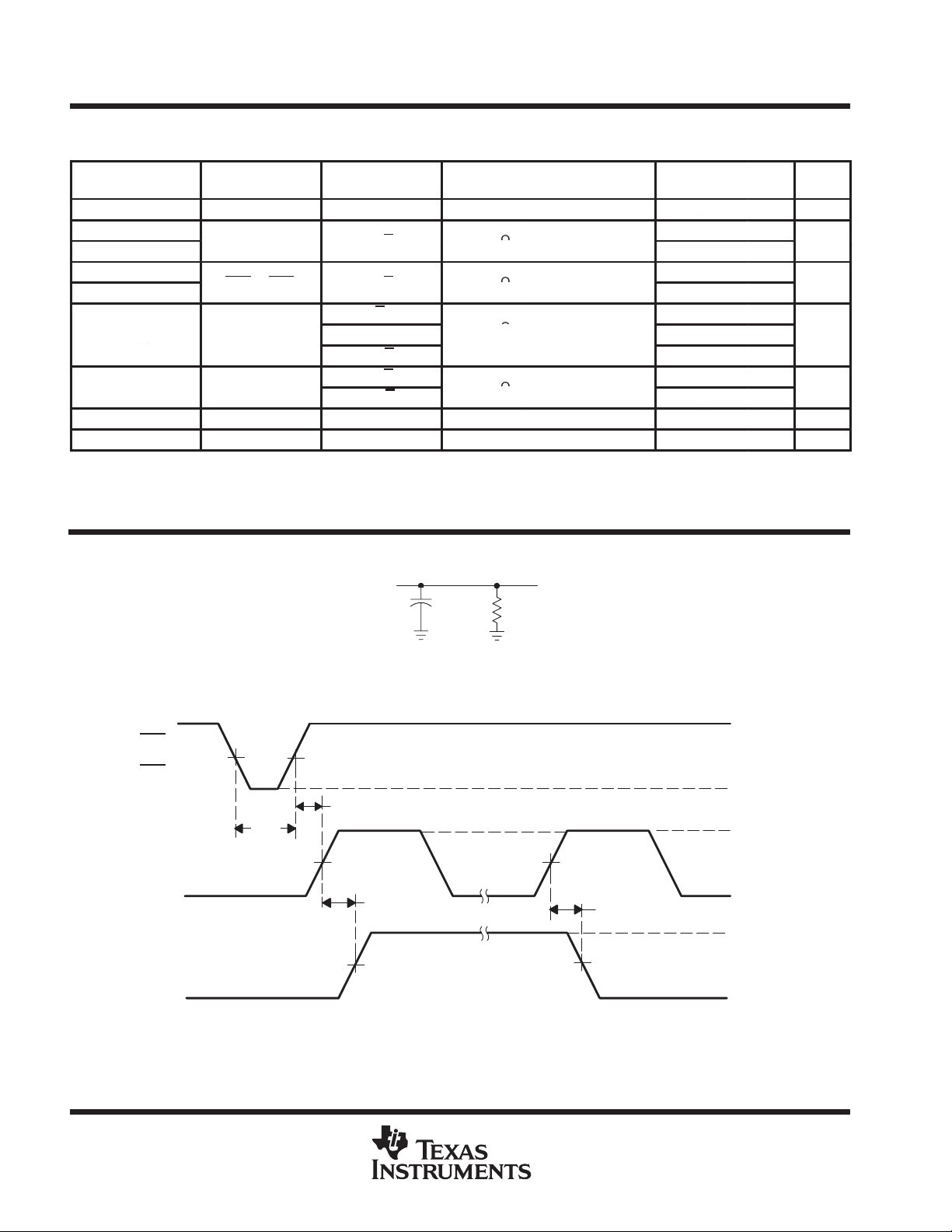
PARAMETER MEASUREMENT INFORMATION
From Output
Under Test
R
C
(see Note A)
or
t
w
Q
1.3 V
t
su
1.3 V
L
LOAD CIRCUIT
t
PLH
1.3 V 1.3 V
L
Test Point
1.3 V
t
PHL
3.5 V
0.3 V
3.5 V
0.3 V
V
OH
V
OL
NOTES: A. CL includes probe and jig capacitance.
B. Input pulses are supplied by generators having the following characteristics: PRR ≤ 10 MHz, tr = 2.5 ns, tf = 2.5 ns.
Figure 1. Load Circuit and Voltage Waveforms
4
POST OFFICE BOX 655303 • DALLAS, TEXAS 75265
Page 5

CDC305
OCTAL DIVIDE-BY-2 CIRCUIT/CLOCK DRIVER
SCAS326A – JUNE 1990 – REVISED NOVEMBER 1995
PARAMETER MEASUREMENT INFORMATION
1
CLR, PRE
0
CLK
t
PHL1
Q1
t
PLH1
Q2
Q3
Q4
Q
Q
Q
t
PLH2
t
PLH3
t
PLH4
t
PHL5
5
t
PHL6
6
t
PHL7
7
t
PHL8
t
PLH5
t
PLH6
t
PLH7
t
PLH8
t
PHL2
t
PHL3
t
PHL4
NOTES: A. t
B. t
C. t
D. t
8
Q
CLK to Q are calculated as the greater of:
sk(o)
– The difference between the fastest and slowest of t
– The difference between the fastest and slowest of t
CLK to Q are calculated as the greater of:
sk(o)
– The difference between the fastest and slowest of t
– The difference between the fastest and slowest of t
CLK to Q and Q
sk(o)
– The difference between the fastest and slowest of t
– The difference between the fastest and slowest of t
is calculated as the greater of | t
sk(p)
are calculated as the greater of:
– t
PLHn
PHLn
Figure 2. Waveforms for Calculation of t
POST OFFICE BOX 655303 • DALLAS, TEXAS 75265
(n = 1, 2, 3, 4)
PLHn
(n = 1, 2, 3, 4)
PHLn
(n = 5, 6, 7, 8)
PLHn
(n = 5, 6, 7, 8)
PHLn
(n = 1, 2, 3, 4), t
PLHn
(n = 1, 2, 3, 4), t
PHLn
| (n = 1, 2, 3, ..., 8).
sk(o)
(n = 5, 6, 7, 8)
PHLn
(n = 5, 6, 7, 8)
PLHn
and t
sk(p)
5
Page 6

PACKAGE OPTION ADDENDUM
www.ti.com
30-Mar-2005
PACKAGING INFORMATION
Orderable Device Status
(1)
Package
Type
Package
Drawing
Pins Package
Qty
Eco Plan
CDC305-1N OBSOLETE PDIP N 16 TBD Call TI Call TI
CDC305D OBSOLETE SOIC D 16 TBD Call TI Call TI
CDC305DR OBSOLETE SOIC D 16 TBD Call TI Call TI
CDC305N OBSOLETE PDIP N 16 TBD Call TI Call TI
(1)
The marketing status values are defined as follows:
ACTIVE: Product device recommended for new designs.
LIFEBUY: TI has announced that the device will be discontinued, and a lifetime-buy period is in effect.
NRND: Not recommended for new designs. Device is in production to support existing customers, but TI does not recommend using this part in
a new design.
PREVIEW: Device has been announced but is not in production. Samples may or may not be available.
OBSOLETE: TI has discontinued the production of the device.
(2)
Eco Plan - The planned eco-friendly classification: Pb-Free (RoHS) or Green (RoHS & no Sb/Br) - please check
http://www.ti.com/productcontent for the latest availability information and additional product content details.
TBD: The Pb-Free/Green conversion plan has not been defined.
Pb-Free (RoHS): TI's terms "Lead-Free" or "Pb-Free" mean semiconductor products that are compatible with the current RoHS requirements
for all 6 substances, including the requirement that lead not exceed 0.1% by weight in homogeneous materials. Where designed to be soldered
at high temperatures, TI Pb-Free products are suitable for use in specified lead-free processes.
Green (RoHS & no Sb/Br): TI defines "Green" to mean Pb-Free (RoHS compatible), and free of Bromine (Br) and Antimony (Sb) based flame
retardants (Br or Sb do not exceed 0.1% by weight in homogeneous material)
(2)
Lead/Ball Finish MSL Peak Temp
(3)
(3)
MSL, Peak Temp. -- The Moisture Sensitivity Level rating according to the JEDEC industry standard classifications, and peak solder
temperature.
Important Information and Disclaimer:The information provided on this page represents TI's knowledge and belief as of the date that it is
provided. TI bases its knowledge and belief on information provided by third parties, and makes no representation or warranty as to the
accuracy of such information. Efforts are underway to better integrate information from third parties. TI has taken and continues to take
reasonable steps to provide representative and accurate information but may not have conducted destructive testing or chemical analysis on
incoming materials and chemicals. TI and TI suppliers consider certain information to be proprietary, and thus CAS numbers and other limited
information may not be available for release.
In no event shall TI's liability arising out of such information exceed the total purchase price of the TI part(s) at issue in this document sold by TI
to Customer on an annual basis.
Addendum-Page 1
Page 7

IMPORTANT NOTICE
Texas Instruments Incorporated and its subsidiaries (TI) reserve the right to make corrections, modifications,
enhancements, improvements, and other changes to its products and services at any time and to discontinue
any product or service without notice. Customers should obtain the latest relevant information before placing
orders and should verify that such information is current and complete. All products are sold subject to TI’s terms
and conditions of sale supplied at the time of order acknowledgment.
TI warrants performance of its hardware products to the specifications applicable at the time of sale in
accordance with TI’s standard warranty. Testing and other quality control techniques are used to the extent TI
deems necessary to support this warranty . Except where mandated by government requirements, testing of all
parameters of each product is not necessarily performed.
TI assumes no liability for applications assistance or customer product design. Customers are responsible for
their products and applications using TI components. To minimize the risks associated with customer products
and applications, customers should provide adequate design and operating safeguards.
TI does not warrant or represent that any license, either express or implied, is granted under any TI patent right,
copyright, mask work right, or other TI intellectual property right relating to any combination, machine, or process
in which TI products or services are used. Information published by TI regarding third-party products or services
does not constitute a license from TI to use such products or services or a warranty or endorsement thereof.
Use of such information may require a license from a third party under the patents or other intellectual property
of the third party, or a license from TI under the patents or other intellectual property of TI.
Reproduction of information in TI data books or data sheets is permissible only if reproduction is without
alteration and is accompanied by all associated warranties, conditions, limitations, and notices. Reproduction
of this information with alteration is an unfair and deceptive business practice. TI is not responsible or liable for
such altered documentation.
Resale of TI products or services with statements different from or beyond the parameters stated by TI for that
product or service voids all express and any implied warranties for the associated TI product or service and
is an unfair and deceptive business practice. TI is not responsible or liable for any such statements.
Following are URLs where you can obtain information on other Texas Instruments products and application
solutions:
Products Applications
Amplifiers amplifier.ti.com Audio www.ti.com/audio
Data Converters dataconverter.ti.com Automotive www.ti.com/automotive
DSP dsp.ti.com Broadband www.ti.com/broadband
Interface interface.ti.com Digital Control www.ti.com/digitalcontrol
Logic logic.ti.com Military www.ti.com/military
Power Mgmt power.ti.com Optical Networking www.ti.com/opticalnetwork
Microcontrollers microcontroller.ti.com Security www.ti.com/security
Telephony www.ti.com/telephony
Video & Imaging www.ti.com/video
Wireless www.ti.com/wireless
Mailing Address: Texas Instruments
Post Office Box 655303 Dallas, Texas 75265
Copyright 2005, Texas Instruments Incorporated
 Loading...