

CDC208
DUAL 1-LINE TO 4-LINE CLOCK DRIVER
WITH 3-STATE OUTPUTS
SCAS109F – APRIL 1990 – REVISED OCTOBER 1998
D
Low-Skew Propagation Delay
Specifications for Clock-Driver
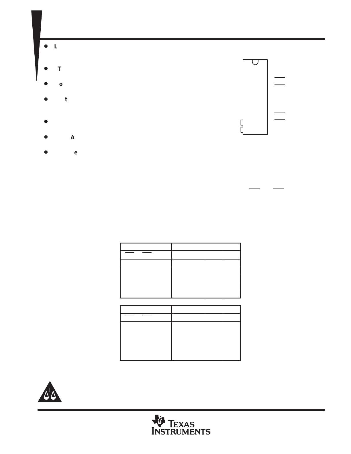
DW PACKAGE
(TOP VIEW)
Applications
D
TTL-Compatible Inputs and
CMOS-Compatible Outputs
D
Flow-Through Architecture Optimizes
PCB Layout
D
Center-Pin VCC and GND Pin
Configurations Minimize High-Speed
Switching Noise
D
EPIC
(Enhanced-Performance Implanted
CMOS) 1-µm Process
D
500-mA Typical Latch-Up Immunity at
1Y2
1Y3
1Y4
GND
GND
GND
GND
2Y1
2Y2
2Y3
1
2
3
4
5
6
7
8
9
10
20
19
18
17
16
15
14
13
12
11
1Y1
1A
1OE1
1OE2
V
CC
V
CC
2A
2OE1
2OE2
2Y4
125°C
D
Package Options Include Plastic
Small-Outline (DW)
description
The CDC208 contains dual clock-driver circuits that fanout one input signal to four outputs with minimum skew
for clock distribution (see Figure 2). The device also offers two output-enable (OE1
circuit that can force the outputs to be disabled to a high-impedance state or to a high- or low-logic level
independent of the signal on the respective A input.
and OE2) inputs for each
Skew parameters are specified for a reduced temperature and voltage range common to many applications.
The CDC208 is characterized for operation from –40°C to 85°C.
FUNCTION TABLES
INPUTS
1OE1 1OE2 1A 1Y1 1Y2 1Y3 1Y4
L L L L L L L
L LHHHHH
LHXLLLL
HLXHHHH
HHXZZZZ
INPUTS OUTPUTS
2OE1 2OE2 2A 2Y1 2Y2 2Y3 2Y4
L L L L L L L
L LHHHHH
LHXLLLL
HLXHHHH
HHXZZZZ
OUTPUTS
Please be aware that an important notice concerning availability, standard warranty, and use in critical applications of
Texas Instruments semiconductor products and disclaimers thereto appears at the end of this data sheet.
EPIC is a trademark of Texas Instruments Incorporated.
PRODUCTION DATA information is current as of publication date.
Products conform to specifications per the terms of Texas Instruments
standard warranty. Production processing does not necessarily include
testing of all parameters.
POST OFFICE BOX 655303 • DALLAS, TEXAS 75265
Copyright 1998, Texas Instruments Incorporated
1
CDC208
DUAL 1-LINE TO 4-LINE CLOCK DRIVER
WITH 3-STATE OUTPUTS
SCAS109F – APRIL 1990 – REVISED OCTOBER 1998
logic symbol
†
This symbol is in accordance with ANSI/IEEE Std 91-1984 and IEC Publication 617-12.
†
1OE1
1OE2
1A
2OE1
2OE2
2A
18
17
19
13
12
14
X/Y
1
2
1
V4
23G5
EN
1
4, 5
4, 5
4, 5
4, 5
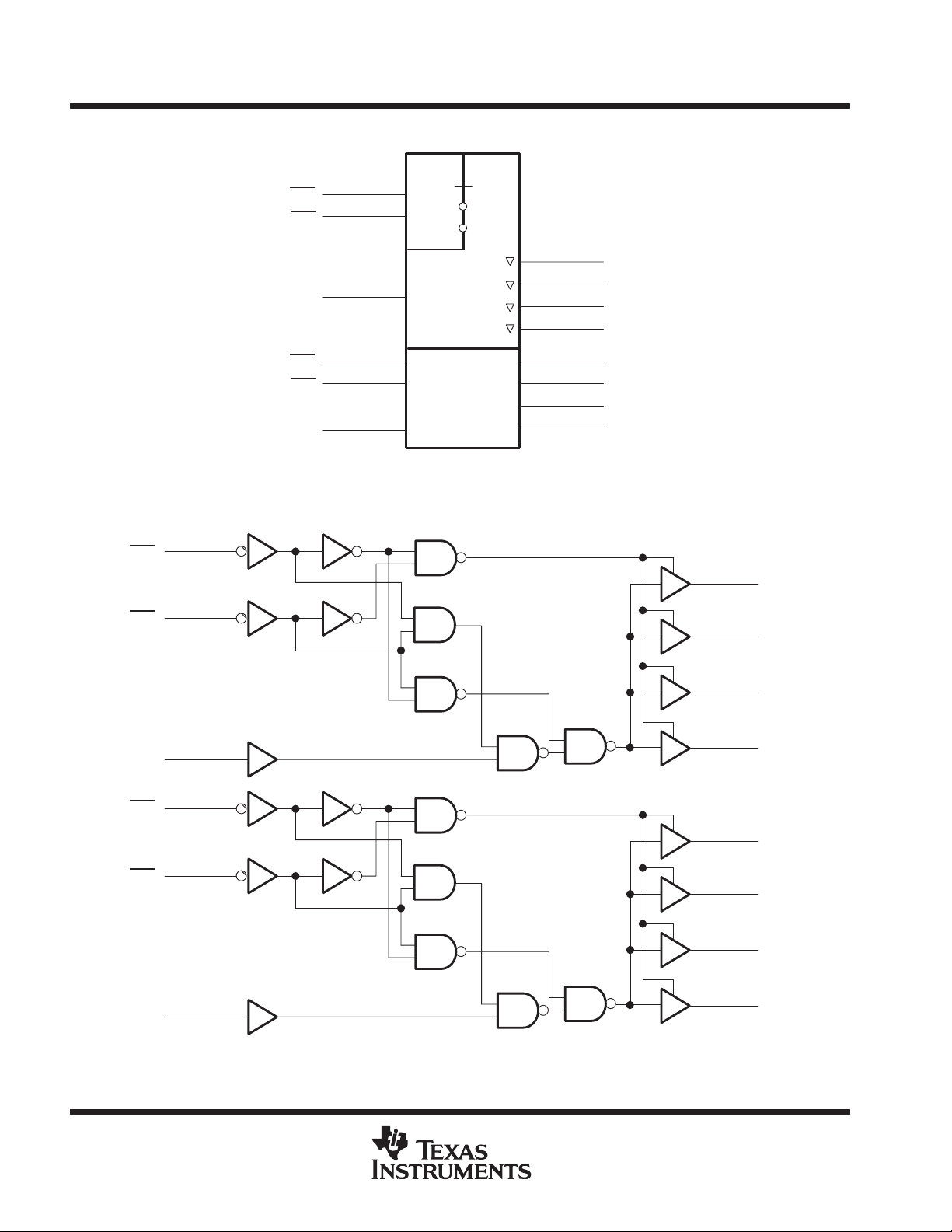
logic diagram (positive logic)
1OE1
1OE2
18
17
20
10
11
1Y1
1
1Y2
2
1Y3
3
1Y4
8
2Y1
9
2Y2
2Y3
2Y4
20
1Y1
1
1Y2
1A
2OE1
2OE2
2A
19
13
12
14
10
11
2
1Y3
3
1Y4
8
2Y1
9
2Y2
2Y3
2Y4
2
POST OFFICE BOX 655303 • DALLAS, TEXAS 75265
CDC208
DUAL 1-LINE TO 4-LINE CLOCK DRIVER
WITH 3-STATE OUTPUTS
SCAS109F – APRIL 1990 – REVISED OCTOBER 1998
absolute maximum ratings over operating free-air temperature range (unless otherwise noted)
Supply voltage range, VCC –0.5 V to 7 V. . . . . . . . . . . . . . . . . . . . . . . . . . . . . . . . . . . . . . . . . . . . . . . . . . . . . . . . . .
Input voltage range, V
Output voltage range, V
Input clamp current, I
Output clamp current, I
Continuous output current, I
Continuous current through V
Maximum power dissipation at T
(see Note 1) –0.5 V to VCC + 0.5 V. . . . . . . . . . . . . . . . . . . . . . . . . . . . . . . . . . . . . . . . . .
I
(see Note 1) –0.5 V to VCC + 0.5 V. . . . . . . . . . . . . . . . . . . . . . . . . . . . . . . . . . . . . . .
O
(VI < 0 or VI > VCC) ±20 mA. . . . . . . . . . . . . . . . . . . . . . . . . . . . . . . . . . . . . . . . . . . . . . . .
IK
(VO < 0 or VO > VCC) ±50 mA. . . . . . . . . . . . . . . . . . . . . . . . . . . . . . . . . . . . . . . . . . . .
OK
(VO = 0 to VCC) ±50 mA. . . . . . . . . . . . . . . . . . . . . . . . . . . . . . . . . . . . . . . . . . . . . .
O
or GND ±200 mA. . . . . . . . . . . . . . . . . . . . . . . . . . . . . . . . . . . . . . . . . . . . . . . . . .
CC
= 55°C (in still air) (see Note 2) 1.6 W. . . . . . . . . . . . . . . . . . . . . . . . . . . . . . .
A
Storage temperature range –65°C to 150°C. . . . . . . . . . . . . . . . . . . . . . . . . . . . . . . . . . . . . . . . . . . . . . . . . . . . . . . .
†
Stresses beyond those listed under “absolute maximum ratings” may cause permanent damage to the device. These are stress ratings only, and
functional operation of the device at these or any other conditions beyond those indicated under “recommended operating conditions” is not
implied. Exposure to absolute-maximum-rated conditions for extended periods may affect device reliability.
NOTES: 1. The input and output negative-voltage ratings may be exceeded if the input and output clamp-current ratings are observed.
2. The maximum package power dissipation is calculated using a junction temperature of 150°C and a board trace length of 750 mils.
For more information, refer to the
Data Book
, literature number SCBD002B.
Package Thermal Considerations
application note in the 1994
ABT Advanced BiCMOS T echnology
recommended operating conditions
MIN NOM MAX UNIT
V
CC
V
IH
V
IL
V
I
I
OH
I
OL
∆t/∆v Input transition rise or fall rate 0 10 ns/V
f
clock
T
A
Supply voltage 4.5 5 5.5 V
High-level input voltage 2 V
Low-level input voltage 0.8 V
Input voltage 0 V
High-level output current –24 mA
Low-level output current 24 mA
Input clock frequency 60 MHz
Operating free-air temperature –40 85 °C
CC
V
†
POST OFFICE BOX 655303 • DALLAS, TEXAS 75265
3
CDC208
PARAMETER
TEST CONDITIONS
V
MIN
MAX
UNIT
I
A
I
mA
I
50 µA
I
24 mA
DUAL 1-LINE TO 4-LINE CLOCK DRIVER
WITH 3-STATE OUTPUTS
SCAS109F – APRIL 1990 – REVISED OCTOBER 1998
electrical characteristics over recommended operating free-air temperature range (unless
otherwise noted)
CC
= –50 µ
OH
V
OH
V
OL
I
I
I
OZ
I
CC
‡
∆I
CC
C
i
C
†
Not more than one output should be tested at a time, and the duration of the test should not exceed 10 ms.
‡
This is the increase in supply current for each input that is at one of the specified TTL voltage levels rather than 0 V or VCC.
o
= –24
OH
IOH = –75 mA
=
OL
=
OL
IOL = 75 mA
VI = VCC or GND 5.5 V ±0.1 ±1 µA
VO = VCC or GND 5.5 V ±0.5 ±5 µA
VI = VCC or GND, IO = 0 5.5 V 8 80 µA
One input at 3.4 V ,
Other inputs at VCC or GND
VI = VCC or GND 5 V 4 pF
VO = VCC or GND 5 V 10 pF
†
†
4.5 V 4.4 4.4
5.5 V 5.4 5.4
4.5 V 3.94 3.8
5.5 V 4.94 4.8
5.5 V 3.85
4.5 V 0.1 0.1
5.5 V 0.1 0.1
4.5 V 0.36 0.44
5.5 V 0.36 0.44
5.5 V 1.65
5.5 V 0.9 1 mA
TA = 25°C
MIN TYP MAX
V
V
4
POST OFFICE BOX 655303 • DALLAS, TEXAS 75265
CDC208
PARAMETER
MIN
MAX
UNIT
1A and 2A
Any Y
ns
,,
Any Y
ns
Any Y
ns
Any Y
ns
1A and 2A
Any Y
ns
CpdPower dissipation capacitance per bank
C
pF
DUAL 1-LINE TO 4-LINE CLOCK DRIVER
WITH 3-STATE OUTPUTS
SCAS109F – APRIL 1990 – REVISED OCTOBER 1998
switching characteristics over recommended operating free-air temperature range,
= 5 V ± 0.5 V (unless otherwise noted) (see Figure 1)
V
CC
FROM TO
(INPUT) (OUTPUT)
t
PLH
t
PHL
t
PLH
t
PHL
t
PZH
t
PZL
t
PHZ
t
PLZ
1OE1, 1OE2, and
2OE1, 2OE2
1OE2 or 2OE2
1OE1 or 2OE1
1OE2 or 2OE2
1OE1 or 2OE1
switching characteristics, VCC = 5 V ± 0.25 V, TA = 25°C to 70°C (see Note 3 and Figures 1 and 2)
PARAMETER
t
PLH
t
PHL
t
sk(o)
NOTE 3: All specifications are valid only for all outputs switching simultaneously and in phase.
FROM
(INPUT)
1A and 2A Any Y 1 ns
(OUTPUT)
TA = 25°C
MIN TYP MAX
5.3 8.5 10.9 5.3 11.7
3.6 7.7 11 3.6 1 1.5
4.7 8.5 11.7 4.7 12.8
4.4 8.4 11.3 4.4 12.4
4.4 8.1 11.3 4.4 12.4
5 9.6 13.3 5 14.9
4.2 7.4 9.3 4.2 10.2
5.4 7.5 9.2 5.4 9.9
TO
MIN MAX UNIT
6.6 10.2
6.6 9.8
operating characteristics, VCC = 5 V, TA = 25°C
PARAMETER TEST CONDITIONS TYP UNIT
p
p
p
Outputs enabled
Outputs disabled
p
= 50 pF, f = 1 MHz
L
96
12
p
POST OFFICE BOX 655303 • DALLAS, TEXAS 75265
5
CDC208
DUAL 1-LINE TO 4-LINE CLOCK DRIVER
WITH 3-STATE OUTPUTS
SCAS109F – APRIL 1990 – REVISED OCTOBER 1998
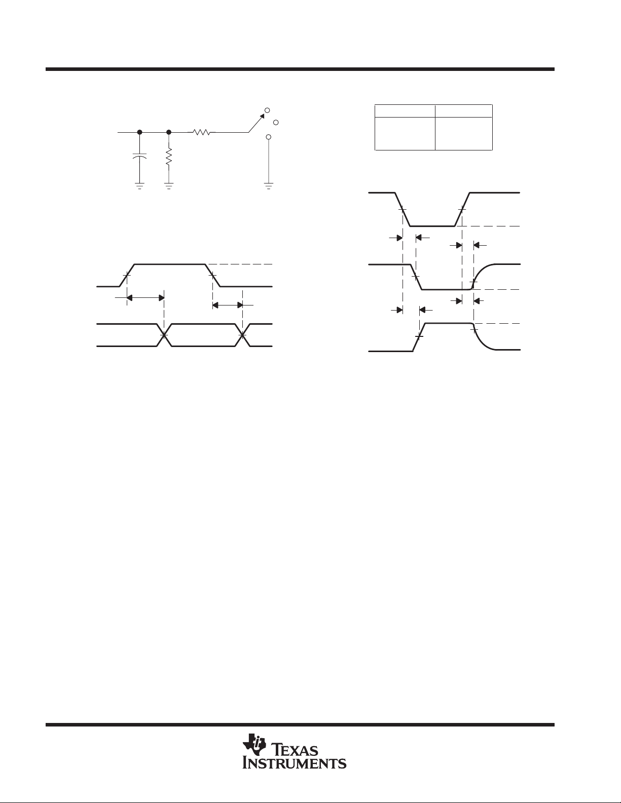
PARAMETER MEASUREMENT INFORMATION
From Output
Under Test
CL = 50 pF
(see Note A)
500 Ω
500 Ω
S1
2 × V
Open
GND
CC
TEST
t
PLH/tPHL
t
PLZ/tPZL
t
PHZ/tPZH
S1
Open
2 × V
GND
CC
(see Note A)
Input
(see Note B)
t
PLH
Output
NOTES: A. CL includes probe and jig capacitance.
B. All input pulses are supplied by generators having the following characteristics: PRR ≤ 10 MHz, ZO = 50 Ω, tr ≤ 3 ns, tf≤ 3 ns.
For testing pulse duration: tr = tf = 1 to 3 ns. Pulse polarity can be either high-to-low-to-high or low-to-high-to-low.
C. Waveform 1 is for an output with internal conditions such that the output is low except when disabled by the output control.
Waveform 2 is for an output with internal conditions such that the output is high except when disabled by the output control.
LOAD CIRCUIT FOR OUTPUTS
1.5 V 1.5 V
50% V
CC
VOLTAGE WAVEFORMS
PROPAGATION DELAY TIMES
Figure 1. Load Circuit and Voltage Waveforms
t
PHL
50% V
3 V
0 V
V
CC
V
OH
OL
Output
Control
(low-level
enabling)
Output
Waveform 1
S1 at 2 × V
(see Note C)
Output
Waveform 2
S1 at 2 × V
(see Note C)
CC
CC
t
PZL
t
PZH
VOLTAGE WAVEFORMS
ENABLE AND DISABLE TIMES
t
PLZ
50% V
t
PHZ
50% V
CC
CC
1.5 V1.5 V
20% V
80% V
CC
CC
3 V
0 V
≈ V
V
V
0 V
CC
OL
OH
6
POST OFFICE BOX 655303 • DALLAS, TEXAS 75265
1A, 2A
CDC208
DUAL 1-LINE TO 4-LINE CLOCK DRIVER
WITH 3-STATE OUTPUTS
SCAS109F – APRIL 1990 – REVISED OCTOBER 1998
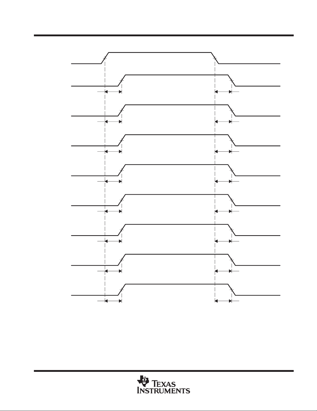
PARAMETER MEASUREMENT INFORMATION
1Y1
1Y2
1Y3
1Y4
2Y1
2Y2
t
PLH1
t
PLH2
t
PLH3
t
PLH4
t
PLH5
t
PLH6
t
PHL1
t
PHL2
t
PHL3
t
PHL4
t
PHL5
t
PHL6
2Y3
2Y4
NOTE A: Output skew, t
– The difference between the fastest and slowest of t
– The difference between the fastest and slowest of t
t
PLH7
t
PLH8
, is calculated as the greater of:
sk(o)
Figure 2. Waveforms for Calculation of t
(n = 1, 2,..., 8)
PLHn
(n = 1, 2,..., 8)
PHLn
POST OFFICE BOX 655303 • DALLAS, TEXAS 75265
sk(o)
t
PHL7
t
PHL8
7
CDC208
DUAL 1-LINE TO 4-LINE CLOCK DRIVER
WITH 3-STATE OUTPUTS
SCAS109F – APRIL 1990 – REVISED OCTOBER 1998
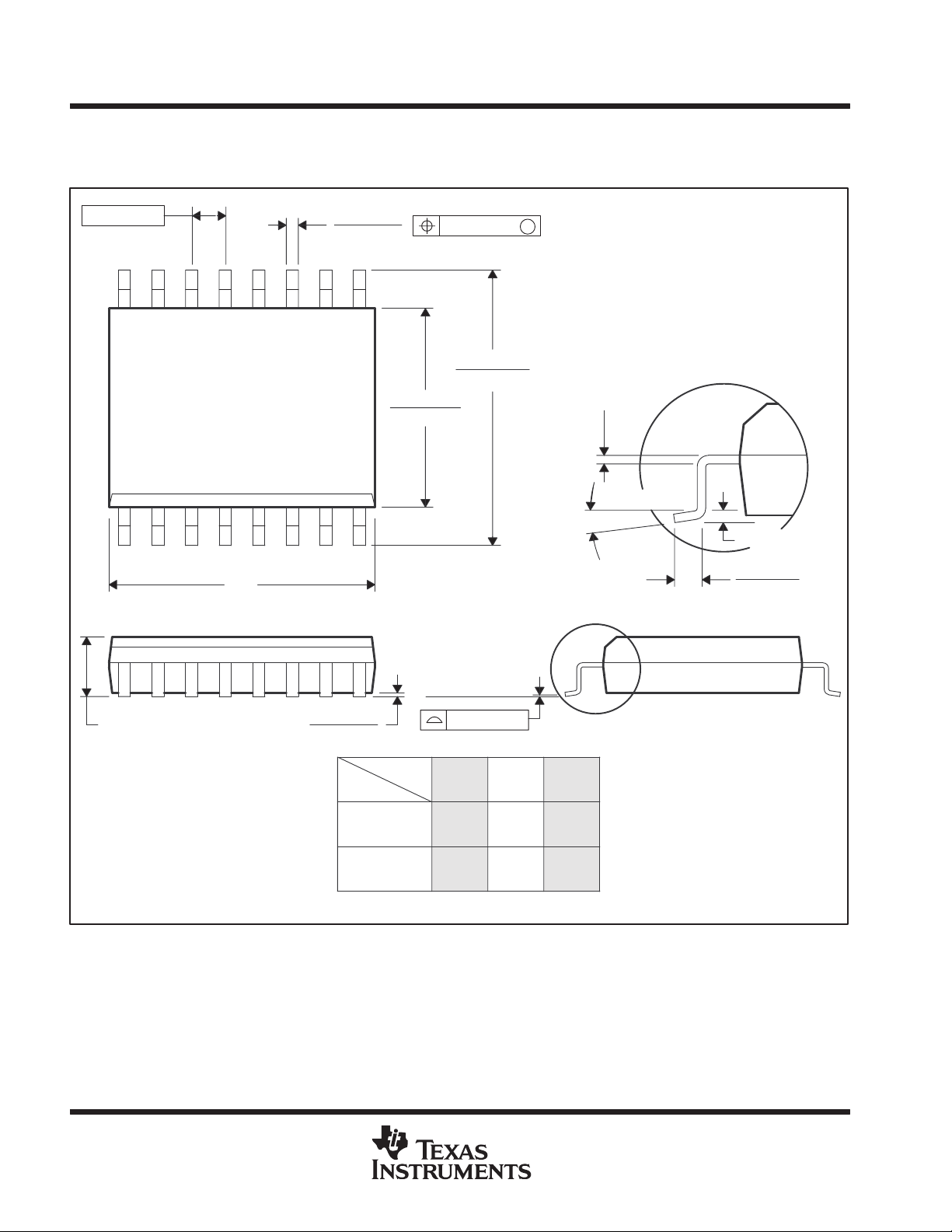
MECHANICAL INFORMATION
DW (R-PDSO-G**) PLASTIC SMALL-OUTLINE PACKAGE
16 PIN SHOWN
0.050 (1,27)
16
1
0.020 (0,51)
0.014 (0,35)
9
0.299 (7,59)
0.293 (7,45)
8
A
0.010 (0,25)
0.419 (10,65)
0.400 (10,15)
M
0.010 (0,25) NOM
0°–8°
Gage Plane
0.010 (0,25)
0.050 (1,27)
0.016 (0,40)
0.104 (2,65) MAX
NOTES: A. All linear dimensions are in inches (millimeters).
B. This drawing is subject to change without notice.
C. Body dimensions do not include mold flash or protrusion not to exceed 0.006 (0,15).
D. Falls within JEDEC MS-013
0.012 (0,30)
0.004 (0,10)
PINS **
DIM
A MAX
A MIN
Seating Plane
0.004 (0,10)
16
0.410
(10,41)
0.400
(10,16)
0.510
(12,95)
0.500
(12,70)
20
24
0.610
(15,49)
0.600
(15,24)
4040000/D 02/98
8
POST OFFICE BOX 655303 • DALLAS, TEXAS 75265

IMPORTANT NOTICE
T exas Instruments and its subsidiaries (TI) reserve the right to make changes to their products or to discontinue
any product or service without notice, and advise customers to obtain the latest version of relevant information
to verify, before placing orders, that information being relied on is current and complete. All products are sold
subject to the terms and conditions of sale supplied at the time of order acknowledgement, including those
pertaining to warranty, patent infringement, and limitation of liability.
TI warrants performance of its semiconductor products to the specifications applicable at the time of sale in
accordance with TI’s standard warranty. Testing and other quality control techniques are utilized to the extent
TI deems necessary to support this warranty . Specific testing of all parameters of each device is not necessarily
performed, except those mandated by government requirements.
CERT AIN APPLICATIONS USING SEMICONDUCTOR PRODUCTS MAY INVOLVE POTENTIAL RISKS OF
DEATH, PERSONAL INJURY, OR SEVERE PROPERTY OR ENVIRONMENTAL DAMAGE (“CRITICAL
APPLICATIONS”). TI SEMICONDUCTOR PRODUCTS ARE NOT DESIGNED, AUTHORIZED, OR
WARRANTED TO BE SUITABLE FOR USE IN LIFE-SUPPORT DEVICES OR SYSTEMS OR OTHER
CRITICAL APPLICA TIONS. INCLUSION OF TI PRODUCTS IN SUCH APPLICATIONS IS UNDERST OOD TO
BE FULLY AT THE CUSTOMER’S RISK.
In order to minimize risks associated with the customer’s applications, adequate design and operating
safeguards must be provided by the customer to minimize inherent or procedural hazards.
TI assumes no liability for applications assistance or customer product design. TI does not warrant or represent
that any license, either express or implied, is granted under any patent right, copyright, mask work right, or other
intellectual property right of TI covering or relating to any combination, machine, or process in which such
semiconductor products or services might be or are used. TI’s publication of information regarding any third
party’s products or services does not constitute TI’s approval, warranty or endorsement thereof.
Copyright 1998, Texas Instruments Incorporated
 Loading...