

Data sheet acquired from Harris Semiconductor
/
j
SCHS127
February 1998
CD74HCU04
High Speed CMOS Logic
Hex Inverter
[ /Title
(CD74
HCU04
)
Sub-
ect
(High
Speed
CMOS
Logic
Hex
Inverter
Features
• Typical Propagation Delay: 6ns at VCC = 5V,
C
= 15pF, TA = 25oC, Fastest Part in QMOS Line
L
o
• Wide Operating Temperature Range . . . -55
• Balanced Propagation Delay and Transition Times
• Significant Power Reduction Compared to LSTTL
Logic ICs
• HCU Types
- 2V to 6V Operation
- High Noise Immunity: N
V
at VCC = 5V
CC
• CMOS Input Compatibility, I
= 20%, NIH = 30% of
IL
≤ 1µA at VOL, V
l
C to 125oC
OH
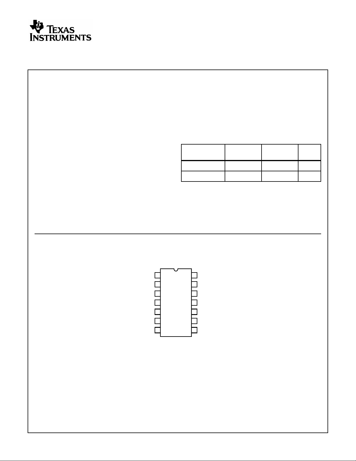
Pinout
Description
The Harris CD74HCU04 unbuffered hexinverter utilizes silicongate CMOS technology to achieve operation speeds similar to
LSTTL gates with the low power consumption of standard
CMOS integrated circuits. These devices are especially useful
in crystal oscillator and analog applications. Figures 10 and 11
are supplied as design information for the above applications .
Ordering Information
TEMP.RANGE
PART NUMBER
CD74HCU04E -55 to 125 14 Ld PDIP E14.3
CD74HCU04M -55 to 125 14 Ld SOIC M14.15
NOTES:
1. When ordering, use theentire part number. Add thesuffix 96 to
obtain the variant in the tape and reel.
2. Waferor dieforthis partnumber is availablewhich meetsallelectrical specifications. Please contact your local sales office or
Harris customer service for ordering information.
(oC) PACKAGE
PKG.
NO.
1A
1Y
2A
2Y
3A
3Y
GND
CD74HC04,
(PDIP, SOIC)
TOP VIEW
1
2
3
4
5
6
7
14
V
CC
6A
13
12
6Y
5A
11
5Y
10
4A
9
4Y
8
CAUTION: These devices are sensitive to electrostatic discharge. Users should follow proper IC Handling Procedures.
Copyright
© Harris Corporation 1998
1
File Number 1655.1
Functional Diagram
CD74HCU04
Logic Symbol
1A
1Y
2A
2Y
3A
3Y
GND
1
2
3
4
5
6
7
14
V
CC
13
6A
12
6Y
11
5A
10
5Y
9
4A
8
4Y
Schematic Diagram
nA nY
(3, 5, 9, 11, 13) 1
V
CC
2 (4, 6, 8, 10, 12)
2
CD74HCU04
Absolute Maximum Ratings Thermal Information
DC Supply Voltage, V
CC
Voltages Referenced to Ground . . . . . . . . . . . . . . . . -0.5V to +7V
DC Input Diode Current, I
IK
For VI < -0.5V or VI > VCC + 0.5V. . . . . . . . . . . . . . . . . . . . . .±20mA
DC Output Diode Current, I
OK
For VO < -0.5V or VO > VCC + 0.5V . . . . . . . . . . . . . . . . . . . .±20mA
DC Drain Current, per Output, I
O
For VO > -0.5V or VO < VCC + 0.5V . . . . . . . . . . . . . . . . . . . .±25mA
DC VCC or Ground Current, ICC . . . . . . . . . . . . . . . . . . . . . . . . .±50mA
Operating Conditions
Temperature Range TA. . . . . . . . . . . . . . . . . . . . . . . -55oC to 125oC
Supply Voltage Range, VCC. . . . . . . . . . . . . . . . . . . . . . . . .2V to 6V
DC Input or Output Voltage, VI, VO . . . . . . . . . . . . . . . . . 0V to V
Input Rise and Fall Time
2V . . . . . . . . . . . . . . . . . . . . . . . . . . . . . . . . . . . . . . 1000ns (Max)
4.5V. . . . . . . . . . . . . . . . . . . . . . . . . . . . . . . . . . . . . . 500ns (Max)
6V . . . . . . . . . . . . . . . . . . . . . . . . . . . . . . . . . . . . . . . 400ns (Max)
CAUTION: Stresses above those listed in “Absolute Maximum Ratings” maycause permanent damage to the device. This is a stress only rating and operation
of the device at these or any other conditions above those indicated in the operational sections of this specification is not implied.
NOTE:
3. θJA is measured with the component mounted on an evaluation PC board in free air.
Thermal Resistance (Typical, Note 3) θJA (oC/W)
PDIP Package. . . . . . . . . . . . . . . . . . . . . . . . . . . . . 100
SOIC Package. . . . . . . . . . . . . . . . . . . . . . . . . . . . . 180
Maximum Junction Temperature (Hermetic P ac kage or Die) . . . 175oC
Maximum Junction Temperature (Plastic Package) . . . . . . . . 150oC
Maximum Storage Temperature Range . . . . . . . . . .-65oC to 150oC
Maximum Lead Temperature (Soldering 10s). . . . . . . . . . . . . 300oC
(SOIC - Lead Tips Only)
CC
DC Electrical Specifications
PARAMETER SYMBOL
High Level Input
Voltage
Low Level Input
Voltage
High Level Output
Voltage
CMOS Loads
High Level Output
Voltage
TTL Loads
Low Level Output
Voltage
CMOS Loads
Low Level Output
Voltage
TTL Loads
Input Leakage
Current
Quiescent Device
Current
V
IH
V
IL
V
OH
V
OL
I
I
I
CC
TEST
CONDITIONS
25oC -40oC TO +85oC -55oC TO 125oC
VCC (V)
- - 2 1.7 - 1.7 - 1.7 - V
4.5 3.6 - 3.6 - 3.6 - V
6 4.8 - 4.8 - 4.8 - V
- - 2 - 0.3 - 0.3 - 0.3 V
4.5 - 0.8 - 0.8 - 0.8 V
6 - 1.1 - 1.1 - 1.1 V
V
IH or
V
-0.02 2 1.8 - 1.8 - 1.8 - V
IL
-0.02 4.5 4 - 4 - 4 - V
-0.02 6 5.5 - 5.5 - 5.5 - V
VCC or
GND
V
IH or
V
IL
-4 4.5 3.98 - 3.84 - 3.7 - V
-5.2 6 5.48 - 5.34 - 5.2 - V
0.02 2 - 0.2 - 0.2 - 0.2 V
0.02 4.5 - 0.5 - 0.5 - 0.5 V
0.02 6 - 0.5 - 0.5 - 0.5 V
4 4.5 - 0.26 - 0.33 - 0.4 V
VCC or
5.2 6 - 0.26 - 0.33 - 0.4 V
GND
VCC or
-6-±0.1 - ±1-±1 µA
GND
VCC or
06-2-20-40µA
GND
UNITSVI(V) IO(mA) MIN MAX MIN MAX MIN MAX
3

CD74HCU04
Switching Specifications Input t
PARAMETER SYMBOL
Propagation Delay,
Input to Output Y (Figure 1)
t
PLH
, tf = 6ns
r
, t
PHLCL
TEST
CONDITIONS
= 50pF 2 - - 70 - 90 - 105 ns
V
CC
(V)
CL = 50pF 4.5 - - 14 - 18 - 21 ns
CL = 15pF 5 - 5 - ----ns
CL = 50pF 6 - - 12 - 15 - 18 ns
Transition Times (Figure 1) t
TLH
, t
THLCL
= 50pF 2 - - 75 - 95 18 110 ns
4.5 - - 15 - 19 - 22 ns
6 - - 13 - 16 - 19 ns
Input Capacitance C
Power Dissipation Capacitance
C
I
PD
- See Figure 3 pF
- 5-14-----pF
(Notes 4, 5)
NOTES:
4. CPD is used to determine the dynamic power consumption, per inverter.
5. PD = V
2
fi (CPD + CL) where fi = input frequency, CL = output load capacitance, VCC = supply voltage.
CC
Test Circuits and Waveforms
tr = 6ns tf = 6ns
INPUT
90%
50%
10%
25oC -40oC TO 85oC -55oC TO125oC
V
CC
GND
UNITSMIN TYP MAX MIN MAX MIN MAX
FIGURE 1. HC AND HCU TRANSITION TIMES AND PROPAGATION DELAY TIMES, COMBINATION LOGIC
Typical Performance Curves
TO GND CURRENT (mA)
CC
V
CC,
I
t
THL
INVERTING
OUTPUT
t
PHL
25.0
22.5
20.0
17.5
15.0
12.5
10.0
7.5
5.0
2.5
0123456
VCC = 2V
t
PLH
VI, INPUT VOLTAGE (V)
t
TLH
90%
50%
10%
AMBIENT TEMPERATURE
TA = 25o C
VCC = 6V
VCC = 4.5V
FIGURE 2. TYPICAL INVERTER SUPPLY CURRENT ASFUNCTION OF INPUT VOLTAGE
4
CD74HCU04
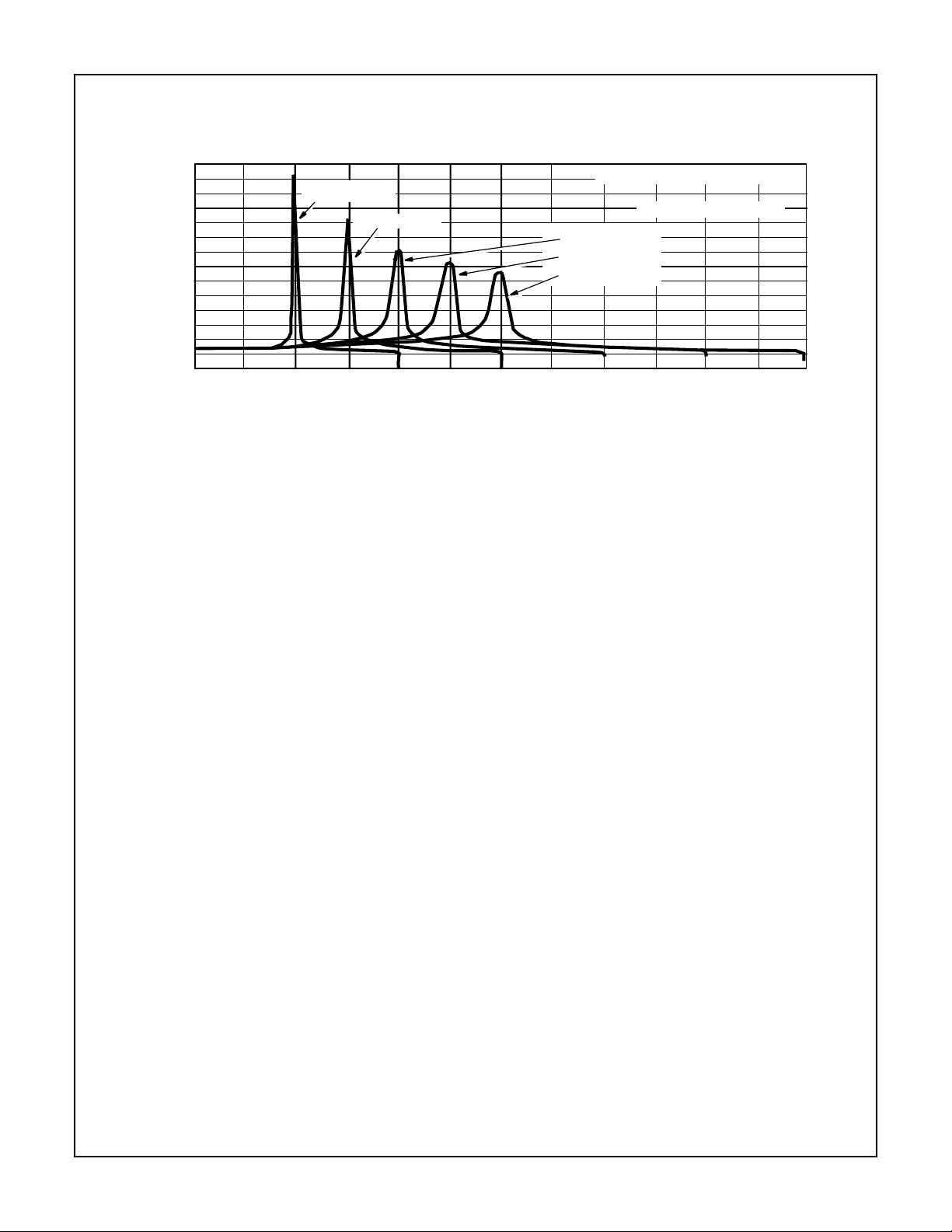
Typical Performance Curves
70
65
60
55
50
45
40
35
30
25
20
, INPUT CAPACITANCE (pF)
I
15
C
10
5
0
VDD = 2V, VI 0-2V
123456
FIGURE 3. INPUT CAPACITNCE AS A FUNCTION OF INPUT VOLTAGE
(Continued)
VDD = 3V, VI 0-3V
V
INPUT VOLTAGE (V)
IN,
AMBIENT TEMPERATURE, TA = 25oC
INPUT PIN 5 CONDITIONS
VDD = 4V, VI 0-4V
V
= 5V, VI 0-5V
DD
= 6V, VI 0-6V
V
DD
5

IMPORTANT NOTICE
T exas Instruments and its subsidiaries (TI) reserve the right to make changes to their products or to discontinue
any product or service without notice, and advise customers to obtain the latest version of relevant information
to verify, before placing orders, that information being relied on is current and complete. All products are sold
subject to the terms and conditions of sale supplied at the time of order acknowledgement, including those
pertaining to warranty, patent infringement, and limitation of liability.
TI warrants performance of its semiconductor products to the specifications applicable at the time of sale in
accordance with TI’s standard warranty. Testing and other quality control techniques are utilized to the extent
TI deems necessary to support this warranty . Specific testing of all parameters of each device is not necessarily
performed, except those mandated by government requirements.
CERTAIN APPLICATIONS USING SEMICONDUCTOR PRODUCTS MAY INVOLVE POTENTIAL RISKS OF
DEATH, PERSONAL INJURY, OR SEVERE PROPERTY OR ENVIRONMENTAL DAMAGE (“CRITICAL
APPLICATIONS”). TI SEMICONDUCTOR PRODUCTS ARE NOT DESIGNED, AUTHORIZED, OR
WARRANTED TO BE SUITABLE FOR USE IN LIFE-SUPPORT DEVICES OR SYSTEMS OR OTHER
CRITICAL APPLICA TIONS. INCLUSION OF TI PRODUCTS IN SUCH APPLICATIONS IS UNDERST OOD TO
BE FULLY AT THE CUSTOMER’S RISK.
In order to minimize risks associated with the customer’s applications, adequate design and operating
safeguards must be provided by the customer to minimize inherent or procedural hazards.
TI assumes no liability for applications assistance or customer product design. TI does not warrant or represent
that any license, either express or implied, is granted under any patent right, copyright, mask work right, or other
intellectual property right of TI covering or relating to any combination, machine, or process in which such
semiconductor products or services might be or are used. TI’s publication of information regarding any third
party’s products or services does not constitute TI’s approval, warranty or endorsement thereof.
Copyright 1998, Texas Instruments Incorporated
 Loading...