

Datasheet CD74HCT40103M96, CD74HCT40103M, CD74HCT40103E, CD74HC40103M96, CD74HC40103M Datasheet (Texas Instruments)
...
CD74HC40103,
[ /Title
(CD74H
C40103,
CD74H
CT4010
3)
/Subject
(High
Speed
CMOS
Logic 8-
Data sheet acquired from Harris Semiconductor
SCHS221
November 1997
Features
• Synchronous or Asynchronous Preset
• Cascadable in Synchronous or Ripple Mode
• Fanout (Over Temperature Range)
- Standard Outputs. . . . . . . . . . . . . . . 10 LSTTL Loads
- Bus Driver Outputs . . . . . . . . . . . . . 15 LSTTL Loads
• Wide Operating Temperature Range . . . -55
• Balanced Propagation Delay and Transition Times
• Significant Power Reduction Compared to LSTTL
Logic ICs
• HC Types
- 2V to 6V Operation
- High Noise Immunity: N
at VCC = 5V
• HCT Types
- 4.5V to 5.5V Operation
- Direct LSTTL Input Logic Compatibility,
V
= 0.8V (Max), VIH = 2V (Min)
IL
- CMOS Input Compatibility, I
= 30%, NIH = 30% of V
IL
≤ 1µA at VOL, V
l
o
C to 125oC
Ordering Information
PART NUMBER TEMP. RANGE (oC) PACKAGE
CD74HC40103E -55 to 125 16 Ld PDIP E16.3
CD74HCT40103E -55 to 125 16 Ld PDIP E16.3
CD74HC40103M -55 to 125 16 Ld SOIC M16.15
CD74HCT40103M -55 to 125 16 Ld SOIC M16.15
NOTES:
1. When ordering, use the entire partnumber. Add the suffix 96 to
obtain the variant in the tape and reel.
2. Wafer ordiefor this partnumber is availablewhich meets allelectrical specifications. Please contact your local sales office or
Harris customer service for ordering information.
OH
CC
PKG.
NO.
CD74HCT40103
High Speed CMOS Logic
8-Stage Synchronous Down Counters
Description
The Harris CD74HC40103 and CD74HCT40103 are
manufactured with high speed silicon gate technology and
consist of an 8-stage synchronous down counter with a
single output which is active when the internal count is zero.
The 40103 contains a single 8-bit binary counter. Each has
control inputs for enabling or disabling the clock, for clearing
the counter to its maximum count, and for presetting the
counter either synchronously or asynchronously. All control
inputs and the
In normal operation, the counter is decremented by one
count on each positive transition of the CLOCK (CP).
Counting is inhibited when the
output goes low when the count reaches zero if the
is low, and remains low for one full clock period.
When the
clocked into the counter on the next positive clock transition
regardless of the state of the
low, data at the P0-P7 inputs are asynchronously forced into
the counter regardless of the state of the
inputs. Input P0-P7 represent a single 8-bit binary word for
the 40103. When the MR input is low, the counter is
asynchronously cleared to its maximum count of 255
regardless of the state of any other input. The precedence
relationship between control inputs is indicated in the truth
table.
If all control inputs except
count, the counters will jump to the maximum count, giving a
counting sequence of 100 or 256 clock pulses long.
The 40103 may be cascaded using the
output, in either a synchronous or ripple mode. These
circuits possess the the low power consumption usually
associated with CMOS circuitry, yet have speeds
comparable to low power Schottky TTL circuits and can drive
up to 10 LSTTL loads.
TC output are active-low logic.
TE input is high. The TC
TE input
PE input is low, data at the P0-P7 inputs are
TE input. When the PL input is
PE, TE, or CLOCK
10
TE are high at the time of zero
TE input and the TC
,
CAUTION: These devices are sensitive to electrostatic discharge. Users should follow proper IC Handling Procedures.
Copyright
© Harris Corporation 1997
1
File Number 1596.1

Pinout
Functional Diagram
CD74HC40103, CD74HCT40103
CD74HC40103, CD74HCT40103
(PDIP, SOIC)
TOP VIEW
V
1
CP
2
MR
3
TE
4
P0
5
P1
P2
6
7
P3
GND
8
14
TC
P7
13
P6
12
P5
11
P4
10
P3
7
P2
6
P1
5
P0
4
16
CC
15
PE (SYNC)
14
TC
13
P7
12
P6
P5
11
10
P4
9
PL (ASYNC)
PL
TE
PE
159312 168
CP
MR
CC
V
GND
TRUTH TABLE
CONTROL INPUTS
PRESET MODE ACTIONMR PL PE TE
1111 Synchronous Inhibit Counter
1110 Count Down
1 1 0 X Preset On Next Positive Clock Transition
1 0 X X Asynchronously Preset Asychronously
0 X X X Clear to Maximum Count
NOTE:
1 = High Level.
0 = Low Level.
X = Don’t Care.
Clock connected to clock input.
Synchronous Operation: changes occur on negative-to-positive clock transitions.
Load Inputs: MSB = P7, LSB = P0.
2

CD74HC40103, CD74HCT40103
Absolute Maximum Ratings Thermal Information
DC Supply Voltage, VCC. . . . . . . . . . . . . . . . . . . . . . . . -0.5V to 7V
DC Input Diode Current, I
IK
For VI < -0.5V or VI > VCC + 0.5V. . . . . . . . . . . . . . . . . . . . . .±20mA
DC Output Diode Current, I
OK
For VO < -0.5V or VO > VCC + 0.5V . . . . . . . . . . . . . . . . . . . .±20mA
DC Output Source or Sink Current per Output Pin, I
O
For VO > -0.5V or VO < VCC + 0.5V . . . . . . . . . . . . . . . . . . . .±25mA
DC VCC or Ground Current, ICC . . . . . . . . . . . . . . . . . . . . . . . . .±50mA
Operating Conditions
Temperature Range, TA . . . . . . . . . . . . . . . . . . . . . . -55oC to 125oC
Supply Voltage Range, V
HC Types . . . . . . . . . . . . . . . . . . . . . . . . . . . . . . . . . . . . .2V to 6V
HCT Types . . . . . . . . . . . . . . . . . . . . . . . . . . . . . . . . .4.5V to 5.5V
DC Input or Output Voltage, VI, VO . . . . . . . . . . . . . . . . . 0V to V
Input Rise and Fall Time
2V . . . . . . . . . . . . . . . . . . . . . . . . . . . . . . . . . . . . . . 1000ns (Max)
4.5V. . . . . . . . . . . . . . . . . . . . . . . . . . . . . . . . . . . . . . 500ns (Max)
6V . . . . . . . . . . . . . . . . . . . . . . . . . . . . . . . . . . . . . . . 400ns (Max)
CAUTION: Stresses above those listed in “Absolute Maximum Ratings” may cause permanent damage to the device. This is a stress only rating and operation
of the device at these or any other conditions above those indicated in the operational sections of this specification is not implied.
NOTE:
3. θJA is measured with the component mounted on an evaluation PC board in free air.
CC
Thermal Resistance (Typical, Note 3) θJA (oC/W)
PDIP Package. . . . . . . . . . . . . . . . . . . . . . . . . . . . . 90
SOIC Package. . . . . . . . . . . . . . . . . . . . . . . . . . . . . 160
Maximum Junction Temperature. . . . . . . . . . . . . . . . . . . . . . .150oC
Maximum Storage Temperature Range . . . . . . . . . .-65oC to 150oC
Maximum Lead Temperature (Soldering 10s). . . . . . . . . . . . .300oC
(SOIC - Lead Tips Only)
CC
DC Electrical Specifications
PARAMETER SYMBOL
HC TYPES
High Level Input
Voltage
Low Level Input
Voltage
High Level Output
Voltage
CMOS Loads
High Level Output
Voltage
TTL Loads
Low Level Output
Voltage
CMOS Loads
Low Level Output
Voltage
TTL Loads
Input Leakage
Current
Quiescent Device
Current
V
IH
V
IL
V
OH
V
OL
I
I
I
CC
TEST
CONDITIONS
(V) IO(mA) MIN TYP MAX MIN MAX MIN MAX
I
V
CC
(V)
o
C -40oC TO 85oC -55oCTO125oC
25
UNITSV
- - 2 1.5 - - 1.5 - 1.5 - V
4.5 3.15 - - 3.15 - 3.15 - V
6 4.2 - - 4.2 - 4.2 - V
- - 2 - - 0.5 - 0.5 - 0.5 V
4.5 - - 1.35 - 1.35 - 1.35 V
6 - - 1.8 - 1.8 - 1.8 V
VIHor VIL-0.02 2 1.9 - - 1.9 - 1.9 - V
-0.02 4.5 4.4 - - 4.4 - 4.4 - V
-0.02 6 5.9 - - 5.9 - 5.9 - V
- - ---- - - - V
-4 4.5 3.98 - - 3.84 - 3.7 - V
-5.2 6 5.48 - - 5.34 - 5.2 - V
VIHor VIL0.02 2 - - 0.1 - 0.1 - 0.1 V
0.02 4.5 - - 0.1 - 0.1 - 0.1 V
0.02 6 - - 0.1 - 0.1 - 0.1 V
- - ---- - - - V
4 4.5 - - 0.26 - 0.33 - 0.4 V
5.2 6 - - 0.26 - 0.33 - 0.4 V
VCC or
-6--±0.1 - ±1-±1µA
GND
VCC or
0 6 - - 8 - 80 - 160 µA
GND
3

CD74HC40103, CD74HCT40103
DC Electrical Specifications (Continued)
TEST
CONDITIONS
PARAMETER SYMBOL
HCT TYPES
High Level Input
Voltage
Low Level Input
Voltage
High Level Output
Voltage
V
IH
V
IL
V
OH
CMOS Loads
High Level Output
Voltage
TTL Loads
Low Level Output
Voltage
V
OL
CMOS Loads
Low Level Output
Voltage
TTL Loads
Input Leakage
Current
Quiescent Device
Current
Additional Quiescent
Device Current Per
I
I
I
CC
∆I
CC
Input Pin: 1 Unit Load
NOTE: For dual-supply systems theoretical worst case (V
(V) IO(mA) MIN TYP MAX MIN MAX MIN MAX
I
- - 4.5 to
- - 4.5 to
VIHor VIL-0.02 4.5 4.4 - - 4.4 - 4.4 - V
-4 4.5 3.98 - - 3.84 - 3.7 - V
VIHor VIL0.02 4.5 - - 0.1 - 0.1 - 0.1 V
4 4.5 - - 0.26 - 0.33 - 0.4 V
VCCand
0 5.5 - - ±0.1 - ±1-±1µA
GND
VCC or
0 5.5 - - 8 - 80 - 160 µA
GND
V
CC
- 4.5 to
-2.1
o
C -40oC TO 85oC -55oCTO125oC
V
CC
25
(V)
2--2- 2 - V
5.5
- - 0.8 - 0.8 - 0.8 V
5.5
- 100 360 - 450 - 490 µA
5.5
= 2.4V, VCC = 5.5V) specification is 1.8mA.
I
UNITSV
HCT Input Loading Table
INPUT UNIT LOADS (NOTE)
P0-P7 0.20
TE, MR 0.40
CP 0.60
PE 0.80
PL 1.35
NOTE: Unit Load is ∆ICClimit specified in DC ElectricalTable, e.g.,
360µA max at 25oC.
Prerequisite for Switching Specifications
25
PARAMETER SYMBOL VCC (V)
HC TYPES
CP Pulse Width t
PL Pulse Width t
W
W
2 165 - - 205 - 250 - ns
4.5 33 - - 41 - 50 - ns
628- -35-43-ns
2 125 - - 155 - 190 - ns
4.5 25 - - 31 - 38 - ns
621- -26-32-ns
o
C -40oC TO 85oC -55oC TO 125oC
UNITSMIN TYP MAX MIN MAX MIN MAX
4
CD74HC40103, CD74HCT40103
Prerequisite for Switching Specifications (Continued)
o
C -40oC TO 85oC -55oC TO 125oC
25
PARAMETER SYMBOL VCC (V)
MR Pulse Width t
W
2 125 - - 135 - 190 - ns
4.5 25 - - 31 - 38 - ns
621- -26-32-ns
CP Max. Frequency
(Note 4)
f
CP(MAX)
23--2-2-MHz
4.5 15 - - 12 - 10 - MHz
6 18 - - 14 - 12 - MHz
P to CP Set-up Time t
SU
2 100 - - 125 - 150 - ns
4.5 20 - - 25 - 30 - ns
617- -21-26-ns
PE to CP Set-up Time t
SU
275- -95-110-ns
4.5 15 - - 19 - 22 - ns
613- -16-19-ns
TE to CP Set-up Time t
SU
2 150 - - 190 - 225 - ns
4.5 30 - - 38 - 45 - ns
626- -33-38-ns
P to CP Hold Time t
H
25--5-5-ns
4.55--5-5-ns
65--5-5-ns
TE to CP Hold Time t
H
20--0-0-ns
4.50--0-0-ns
60--0-0-ns
MR to CP Removal Time t
REM
250- -65-75-ns
4.5 10 - - 13 - 15 - ns
6 9 - - 11 - 13 - ns
PE to CP Hold Time t
H
22--2-2-ns
4.52--2-2-ns
62--2-2-ns
HCT TYPES
CP Pulse Width t
PL Pulse Width t
MR Pulse Width t
CP Max. Frequency
(Note 4)
f
CP(MAX)
P to CP Set-up Time t
PE to CP Set-up Time t
TE to CP Set-up Time t
P to CP Hold Time t
TE to CP Hold Time t
MR to CP Removal Time t
W
W
W
SU
SU
SU
H
H
REM
4.5 35 - - 44 - 53 - ns
4.5 43 - - 54 - 65 - ns
4.5 35 - - 44 - 53 - ns
4.5 14 - - 11 - 9 - MHz
4.5 24 - - 30 - 36 - ns
4.5 20 - - 25 - 30 - ns
4.5 40 - - 50 - 60 - ns
4.55--5-5-ns
4.50--0-0-ns
4.5 10 - - 13 - 15 - ns
PE to CP Hold Time tH 4.5 2 - - 2 - 2 - ns
UNITSMIN TYP MAX MIN MAX MIN MAX
5

CD74HC40103, CD74HCT40103
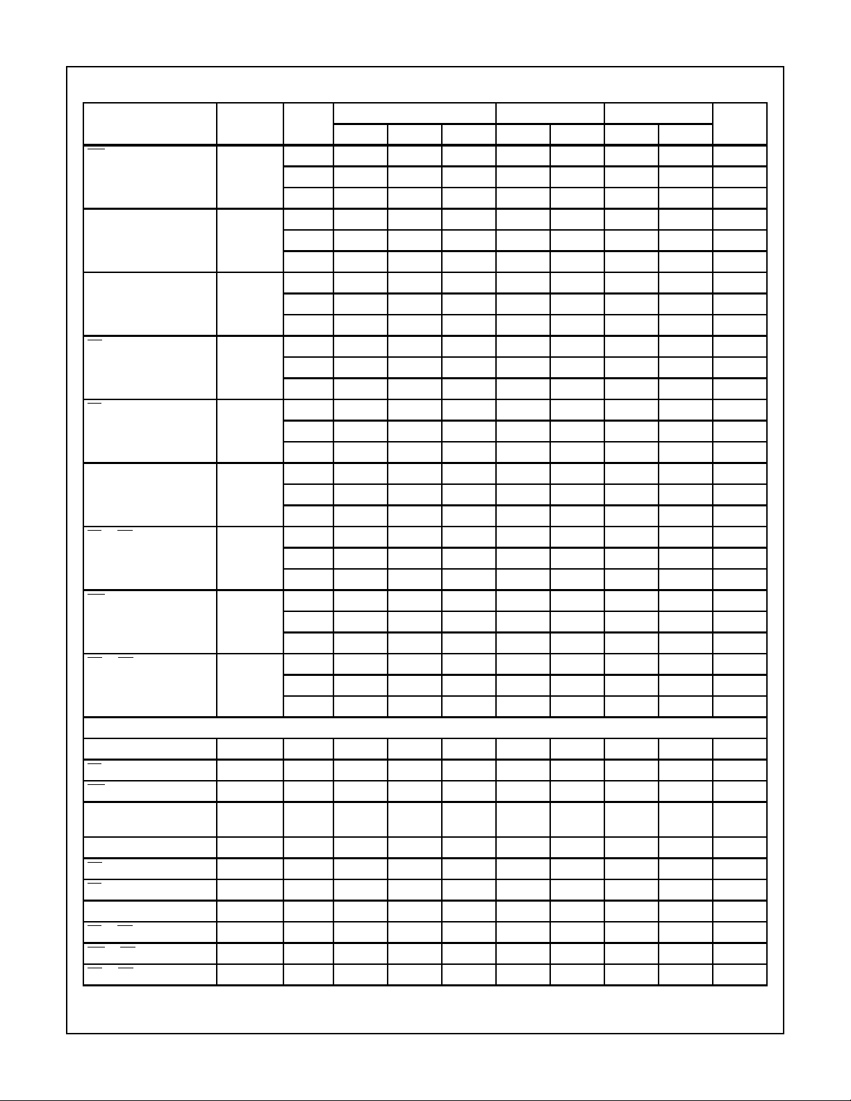
Switching Specifications Input t
PARAMETER SYMBOL
HC TYPES
Propagation Delay t
CP to any
CP to
TE to TC t
PL to TC t
MR to TC t
Output Transition Time t
Input Capacitance C
CP Maximum Frequency f
Power Dissipation Capacitance
(Notes 5, 6)
HCT TYPES
Propagation Delay
CP to
CE to TC (Sync Preset) t
TE to TC t
PL to TC t
TC (Async Preset) CL = 50pF 4.5 - - 60 - 75 - 90 ns
TC (Sync Preset) t
TLH,tTHLCL
TC (Async Preset) t
, tf = 6ns
r
PLH,
t
PHL
PLH,
t
PHL
PLH,
t
PHL
PLH,
t
PHL
PLH,
t
PHL
I
MAX
C
PD
PLH,
t
PHL
PLH,
t
PHL
PLH,
t
PHL
PLH,
t
PHL
TEST
CONDITIONS
o
C
V
CC
25
-40oC TO
85oC
(V)
-55oC TO
125oC
UNITSMIN TYP MAX MIN MAX MIN MAX
CL = 50pF 2 - - 300 - 375 - 450 ns
C
= 15pF 5 - 25 - - - ns
L
C
= 50pF 6 - - 51 - 64 - 77 ns
L
CL = 50pF 2 - - 300 - 375 - 450 ns
C
= 50pF 4.5 - - 60 - 75 - 90 ns
L
C
= 15pF 5 - 25 - - - - - ns
L
C
= 50pF 6 - - 51 - 64 - 77 ns
L
CL = 50pF 2 - - 200 - 250 - 300 ns
C
= 50pF 4.5 - - 40 - 50 - 60 ns
L
C
= 15pF 5 - 17 - - - - - ns
L
C
= 50pF 6 - - 34 - 43 - 51 ns
L
CL = 50pF 2 - - 275 - 345 - 415 ns
C
= 50pF 4.5 - - 55 - 69 - 83 ns
L
C
= 15pF 5 - 23 - - - - - ns
L
C
= 50pF 6 - - 47 - 59 - 71 ns
L
CL = 50pF 2 - - 275 - 345 - 415 ns
C
= 50pF 4.5 - - 55 - 69 - 83 ns
L
C
= 15pF 5 - 23 - - - - - ns
L
C
= 50pF 6 - - 47 - 59 - 71 ns
L
= 50pF 2 - - 75 - 95 - 110 ns
C
= 50pF 4.5 - - 15 - 19 - 22 ns
L
C
= 50pF 6 - - 13 - 16 - 19 ns
L
CL = 50pF - - - 10 - 10 - 10 pF
CL = 15pF 5 - 25 - - - - - MHz
-5-25-----pF
CL = 50pF 4.5 - - 60 - 75 - 90 ns
C
= 15pF 5 - 25 - - - - - ns
L
CL = 50pF 4.5 - - 63 - 79 - 95 ns
C
= 15pF 5 - 26 - - - - - ns
L
CL = 50pF 4.5 - - 50 - 63 - 75 ns
C
= 15pF 5 - 21 - - - - - ns
L
CL = 50pF 4.5 - - 68 - 85 - 102 ns
C
= 15pF 5 - 28 - - - - - ns
L
6

CD74HC40103, CD74HCT40103
Switching Specifications Input t
PARAMETER SYMBOL
MR to TC t
Output Transition Time t
Input Capacitance C
CP Maximum Frequency f
Power Dissipation Capacitance
(Notes 5, 6)
, tf = 6ns (Continued)
r
TEST
CONDITIONS
PLH,
t
PHL
THL,tTLHCL
IN
MAX
C
PD
CL = 50pF 4.5 - - 55 - 69 - 83 ns
C
L
CL = 50pF - - - 10 - 10 - 10 pF
CL = 15pF 5 - 25 - - - - - MHz
o
C
V
CC
25
-40oC TO
85oC
-55oC TO
125oC
(V)
= 15pF 5 - 23 - - - - - ns
= 50pF 4.5 - - 15 - 19 - 22 ns
-5-27-----pF
NOTES:
4. Noncascaded operationonly.With cascaded countersclock-to-terminal count propagationdelays, count enables(
PEor TE)-to-clock SET
UP TIMES, and count enables (PE or TE)-to-clock HOLD TIMES determine maximum clock frequency. For example, with these HC devices:
CPf
------------------------------------------------------------------------------------------------------------------------------------------------------------------------------------
MAX
CP-to-TC prop delay + TE-to-CP Setup Time + TE-to-CP Hold Time
1
1
-----------------------------
60 30 0++
11MHz≈==
5. CPD is used to determine the dynamic power consumption, per package.
6. PD = V
CC
2
fi+ CL V
2
fo where fi = Input Frequency, CL = Output Load Capacitance, VCC = Supply Voltage, fo = Output Frequency.
CC
Timing Diagrams
UNITSMIN TYP MAX MIN MAX MIN MAX
CP
MR
TE
PE
PL
P0
P1
P2
P3
P4
P5
P6
P7
TC
HC/HCT40103 COUNT
255 254 3 2 1 0 255 254 254 253 8 7 6 5 4 255 254 253 252
FIGURE 2.
7

Test Circuits and Waveforms
CD74HC40103, CD74HCT40103
INPUTS
P0 - P7
PE
CP
t
PHL
TC
CP
t
t
r
THL
TE
TC
10%
90%
t
t
f
PHL
10%
10%
90%
t
THL
V
t
90%
f
t
W
1/f
MAX
V
S
V
S
INPUT LEVEL
GND
t
PLH
t
TLH
MR
CP
FIGURE 3. FIGURE 4.
t
f
10%
90%
V
S
V
S
INPUT LEVEL
t
PLH
t
TLH
MR
CP
t
SU
FIGURE 5. FIGURE 6.
VALID
INPUT LEVEL
S
t
t
SU
t
SU
V
S
h
V
S
t
h
t
REC
GND
INPUT LEVEL
GND
INPUT LEVEL
GND
TE
OR
PE
CP
V
S
t
SU
t
W
V
S
t
REM
V
S
V
S
INPUT LEVEL
GND
INPUT LEVEL
GND
INPUT LEVEL
GND
t
h
V
S
INPUT LEVEL
GND
INPUT LEVEL
t
h
V
S
GND
INPUT LEVEL
GND
FIGURE 7. FIGURE 8.
trC
L
CLOCK
10%
90%
50%
10%
tfC
t
WL
L
tWL+ tWH=
50%
t
WH
fC
50%
I
L
V
CC
GND
NOTE: Outputs should be switching from 10% VCC to 90% VCC in
accordance with device truth table.For f
, input duty cycle = 50%.
MAX
FIGURE 9. HC CLOCK PULSE RISE AND FALL TIMES AND
PULSE WIDTH
+ tWH=
t
t
rCL
CLOCK
= 6ns
0.3V
2.7V
1.3V
0.3V
t
t
fCL
WL
= 6ns
1.3V
WL
1.3V
t
WH
NOTE: Outputs should be switching from 10% VCC to 90% VCC in
accordance with device truth table.For f
, input duty cycle = 50%.
MAX
FIGURE 10. HCT CLOCK PULSE RISE AND FALL TIMES AND
PULSE WIDTH
8
I
fC
L
3V
GND

IMPORTANT NOTICE
T exas Instruments and its subsidiaries (TI) reserve the right to make changes to their products or to discontinue
any product or service without notice, and advise customers to obtain the latest version of relevant information
to verify, before placing orders, that information being relied on is current and complete. All products are sold
subject to the terms and conditions of sale supplied at the time of order acknowledgement, including those
pertaining to warranty, patent infringement, and limitation of liability.
TI warrants performance of its semiconductor products to the specifications applicable at the time of sale in
accordance with TI’s standard warranty. Testing and other quality control techniques are utilized to the extent
TI deems necessary to support this warranty . Specific testing of all parameters of each device is not necessarily
performed, except those mandated by government requirements.
CERT AIN APPLICATIONS USING SEMICONDUCTOR PRODUCTS MAY INVOLVE POTENTIAL RISKS OF
DEATH, PERSONAL INJURY, OR SEVERE PROPERTY OR ENVIRONMENTAL DAMAGE (“CRITICAL
APPLICATIONS”). TI SEMICONDUCTOR PRODUCTS ARE NOT DESIGNED, AUTHORIZED, OR
WARRANTED TO BE SUITABLE FOR USE IN LIFE-SUPPORT DEVICES OR SYSTEMS OR OTHER
CRITICAL APPLICA TIONS. INCLUSION OF TI PRODUCTS IN SUCH APPLICATIONS IS UNDERST OOD TO
BE FULLY AT THE CUSTOMER’S RISK.
In order to minimize risks associated with the customer’s applications, adequate design and operating
safeguards must be provided by the customer to minimize inherent or procedural hazards.
TI assumes no liability for applications assistance or customer product design. TI does not warrant or represent
that any license, either express or implied, is granted under any patent right, copyright, mask work right, or other
intellectual property right of TI covering or relating to any combination, machine, or process in which such
semiconductor products or services might be or are used. TI’s publication of information regarding any third
party’s products or services does not constitute TI’s approval, warranty or endorsement thereof.
Copyright 1999, Texas Instruments Incorporated
 Loading...