

Texas Instruments CD74HCT7046AM96, CD74HCT7046AM, CD74HCT7046AE, CD74HC7046AM96, CD74HC7046AM Datasheet
...
CD74HC7046A,
[ /Title
(CD74
HC704
6A,
CD74
HCT70
46A)
/Subject
(PhaseLocked
Loop
Data sheet acquired from Harris Semiconductor
SCHS218
February 1998
Features
• Center Frequency of 18MHz (Typ) at VCC = 5V,
Minimum Center Frequency of 12MHz at V
• Choice of Two Phase Comparators
- Exclusive-OR
- Edge-Triggered JK Flip-Flop
• Excellent VCO Frequency Linearity
• VCO-Inhibit Control for ON/OFF Keying and for Low
Standby Power Consumption
• Minimal Frequency Drift
• Zero Voltage Offset Due to Op-Amp Buffer
• Operating Power-Supply Voltage Range
- VCO Section . . . . . . . . . . . . . . . . . . . . . . . . . . 3V to 6V
- Digital Section . . . . . . . . . . . . . . . . . . . . . . . . 2V to 6V
• Fanout (Over Temperature Range)
- Standard Outputs. . . . . . . . . . . . . . . 10 LSTTL Loads
- Bus Driver Outputs . . . . . . . . . . . . . 15 LSTTL Loads
• Wide Operating Temperature Range . . . -55
• Balanced Propagation Delay and Transition Times
• Significant Power Reduction Compared to LSTTL
Logic ICs
• HC Types
- 2V to 6V Operation
- High Noise Immunity: N
at VCC = 5V
• HCT Types
- 4.5V to 5.5V Operation
- Direct LSTTL Input Logic Compatibility,
V
= 0.8V (Max), VIH = 2V (Min)
IL
- CMOS Input Compatibility, I
= 30%, NIH = 30% of V
IL
≤ 1µA at VOL, V
l
CC = 4.5V
o
C to 125oC
OH
CD74HCT7046A
Phase-Locked Loop
with VCO and Lock Detector
Description
The Harris CD74HC7046A and CD74HCT7046A high-speed
silicon-gate CMOS devices, specified in compliance with
JEDEC Standard No. 7A, are phase-locked-loop (PLL)
circuits that contain a linear voltage-controlled oscillator
(VCO), two-phase comparators (PC1, PC2), and a lock
detector. A signal input and a comparator input are common
to each comparator. The lock detector gives a HIGH level at
pin 1 (LD) when the PLL is locked. The lock detector
capacitor must be connected between pin 15 (C
8 (Gnd). For a frequency range of 100kHz to 10MHz, the
lock detector capacitor should be 1000pF to 10pF,
respectively.
The signal input can be directly coupled to large voltage
signals, or indirectly coupled (with a series capacitor) to
small voltage signals. A self-bias input circuit keeps small
voltage signals within the linear region of the input amplifiers.
With a passive low-pass filter, the 7046A forms a secondorder loop PLL. The excellent VCO linearity is achieved by
the use of linear op-amp techniques.
Ordering Information
TEMP. RANGE
CC
PART NUMBER
CD74HC7046AE -55 to 125 16 Ld PDIP E16.3
CD74HCT7046AE -55 to 125 16 Ld PDIP E16.3
CD74HC7046AM -55 to 125 16 Ld SOIC M16.15
CD74HCT7046AM -55 to 125 16 Ld SOIC M16.15
NOTES:
1. When ordering, use the entire partnumber. Add the suffix 96 to
obtain the variant in the tape and reel.
2. Wafer and die for this part number is available which meets all
electrical specifications. Please contact your local sales office or
Harris customer service for ordering information.
(oC) PACKAGE PKG. NO.
) and pin
LD
Applications
• FM Modulation and Demodulation
• Frequency Synthesis and Multiplication
• Frequency Discrimination
• Tone Decoding
• Data Synchronization and Conditioning
• Voltage-to-Frequency Conversion
• Motor-Speed Control
• Related Literature
- AN8823, CMOS Phase-Locked-Loop Application
Using the CD74HC/HCT7046A and
CD74HC/HCT7046A
CAUTION: These devices are sensitive to electrostatic discharge. Users should follow proper IC Handling Procedures.
Copyright
© Harris Corporation 1998
1
File Number 1920.1
CD74HC7046A, CD74HCT7046A
Pinout
CD74HC7046A, CD74HCT7046A
(PDIP, SOIC)
TOP VIEW
PC1
COMP
VCO
LD
OUT
OUT
INH
C1
C1
GND
1
2
3
IN
4
5
6
A
7
B
8
674314
C1
A
C1
C1
16
15
14
13
12
11
10
9
B
VCO
V
C
SIG
PC2
R
R
DEM
VCO
OUT
CC
LD
2
1
IN
OUT
OUT
IN
COMP
Functional Diagram
2
15
13
1
4
10
OUT
PC1
C
LD
PC2
LD
VCO
DEM
2
OUT
OUT
OUT
OUT
C1
C1
INH
3
IN
14
IN
A
B
11
R
1
12
R
2
IN
φ
6
7
VCO
9
5
PC1
COMP
SIG
VCO
SIG
IN
IN
R2
R1
R5
V
REF
R2
12
R1
11
OUT
10
DEM
+
-
-
+
VCO
-
+
INH
59
VCO
IN
LOCK DETECTOR
CC
V
V
CC
D
CP
D
CP
UP
Q
Q
R
D
Q
DOWN
Q
R
D
1.5K
150Ω
PC2
OUT
V
CC
GND
p
n
LOCK
DETECTOR
1
OUTPUT
15
C
LOCK
DETECTOR
CAPACITOR
13
LD
R3
C2
FIGURE 1. LOGIC DIAGRAM
2
CD74HC7046A, CD74HCT7046A
Pin Descriptions
PIN NO. SYMBOL NAME AND FUNCTION
1 LD Lock Detector Output (Active High)
2 PC1
3 COMP
4 VCO
5 INH Inhibit Input
6C1
7C1
8 Gnd Ground (0V)
9 VCO
10 DEM
11 R
12 R
13 PC2
14 SIG
15 C
16 V
CC
Phase Comparator 1 Output
OUT
Comparator Input
IN
VCO Output
OUT
Capacitor C1 Connection A
A
Capacitor C1 Connection B
B
VCO Input
IN
Demodulator Output
OUT
Resistor R1 Connection
1
Resistor R2 Connection
2
Phase Comparator 2 Output
OUT
Signal Input
IN
Lock Detector Capacitor Input
LD
Positive Supply Voltage
General Description
VCO
The VCO requires one external capacitor C1 (between C1
and C1B) and one external resistor R1 (between R1 and
Gnd) or two external resistors R1 and R2 (between R1 and
Gnd, and R2 and Gnd). Resistor R1 and capacitor C1 determine the frequency range of the VCO. Resistor R2 enables
the VCO to have a frequency offset if required. See logic diagram, Figure 1.
The high input impedance of the VCO simplifies the design
of low-pass filters by giving the designer a wide choice of
resistor/capacitor ranges. In order not to load the low-pass
filter, a demodulator output of the VCO input voltage is provided at pin 10 (DEM
niques where the DEM
lower than the VCO input voltage, here the DEM
equals that of the VCO input. If DEM
resistor (R
unused, DEM
(VCO
input (COMP
) should be connected from DEM
S
OUT
) can be connected directly to the comparator
OUT
), or connected via a frequency-divider. The
IN
VCO output signal has a guaranteed duty factor of 50%. A
LOW level at the inhibit input (INH) enables the VCO, while a
HIGH level disables the VCO to minimize standby power
consumption.
Phase Comparators
The signal input (SIG
biasing amplifier at pin 14, provided that the signal swing is
between the standard HC family input logic levels, Capacitive coupling is required for signals with smaller swings.
). In contrast to conventional tech-
OUT
voltage is one threshold voltage
OUT
is used, a load
OUT
OUT
OUT
to Gnd; if
voltage
should be left open. The VCO output
) can be directly coupled to the self-
IN
Phase Comparator 1 (PC1)
This is an Exclusive-OR network. The signal and comparator
input frequencies (f
) must have a 50% duty factor to obtain
i
the maximum locking range. The transfer characteristic of
PC1, assuming ripple (f
V
DEMOUT
=(VCC/π)(φ
is the demodulator output at pin 10; V
= 2fi) is suppressed, is:
r
SIGIN
- φ
COMPIN
) where V
DEMOUT=VPC1OUT
(via low-pass filter).
The average output voltage from PC1, fed to the VCO input
via the low-pass filter and seen at the demodulator output at
pin 10 (V
DEMOUT
of signals (SIG
shown in Figure 2. The average of V
), is the resultant of the phase differences
) and the comparator input (COMPIN)as
IN
is equal to 1/2 V
DEM
when there is no signal or noise at SIGIN, and with this input
the VCO oscillates at the center frequency (f
forms for the PC1 loop locked at f
The frequency capture range (2f
shown in Figure 3.
o
) is defined as the fre-
c
). Typical wave-
o
quency range of input signals on which the PLL will lock if it
was initially out-of-lock. The frequency lock range (2f
defined as the frequency range of input signals on which the
loop will stay locked if it was initially in lock. The capture
range is smaller or equal to the lock range.
With PC1, the capture range depends on the low-pass filter
characteristics and can be made as large as the lock range.
This configuration retains lock behavior even with very noisy
input signals. Typical of this type of phase comparator is that
it can lock to input frequencies close to the harmonics of the
VCO center frequency.
A
Phase Comparator 2 (PC2)
This is a positive edge-triggered phase and frequency detector. When the PLL is using this comparator, the loop is controlled by positive signal transitions and the duty factors of
SIGIN and COMP
are not important. PC2 comprises two
IN
D-type flip-flops, control-gating and a three-state output
stage. The circuit functions as an up-down counter (Figure
1) where SIG
causes an up-count and COMPINa down-
IN
count. The transfer function of PC2, assuming ripple (f
is suppressed, is:
V
DEMOUT
is the demodulator output at pin 10; V
=(VCC/4π)(φ
SIGN
- φ
COMPIN
) where V
DEMOUT=VPC2OUT
(via low-pass filter).
The average output voltage from PC2, fed to the VCO via the
low-pass filter and seen at the demodulator output at pin 10
(V
DEMOUT
SIG
for the PC2 loop locked at f
When the frequencies of SIG
the phase of SIG
driver at PC2
the phase differences (φ
), is the resultant of the phase differences of
and COMPINas shown in Figure 4. Typical waveforms
IN
leads that of COMPIN, the p-type output
IN
is held “ON” for a time corresponding to
OUT
are shown in Figure 5.
o
and COMPINare equal but
IN
DEMOUT
). When the phase of SIG
lags that of COMPIN, the n-type driver is held “ON”.
When the frequency of SIG
is higher than that of COMPIN,
IN
the p-type output driver is held “ON” for most of the input signal cycle time, and for the remainder of the cycle both n-type
and p-type drivers are “OFF” (three-state). If the SIG
DEMOUT
CC
)is
L
r=fi
DEMOUT
IN
fre-
IN
)
3
CD74HC7046A, CD74HCT7046A
quency is lower than the COMP
frequency, then it is the n-
IN
type driver that is held “ON” for most of the cycle. Subsequently, the voltage at the capacitor (C2) of the low-pass filter
connected to PC2
varies until the signal and comparator
OUT
inputs are equal in both phase and frequency . At this stable
point the voltage on C2 remains constant as the PC2 output is
in three-state and the VCO input at pin 9 is a high impedance.
Thus, for PC2, no phase difference exists between SIG
IN
and COMPINover the full frequency range of the VCO.
Moreover, the power dissipation due to the low-pass filter is
reduced because both p-type and n-type drivers are “OFF”
for most of the signal input cycle. It should be noted that the
PLL lock range for this type of phase comparator is equal to
the capture range and is independent of the low-pass filter.
With no signal present at SIG
, the VCO adjusts, via PC2,
IN
to its lowest frequency.
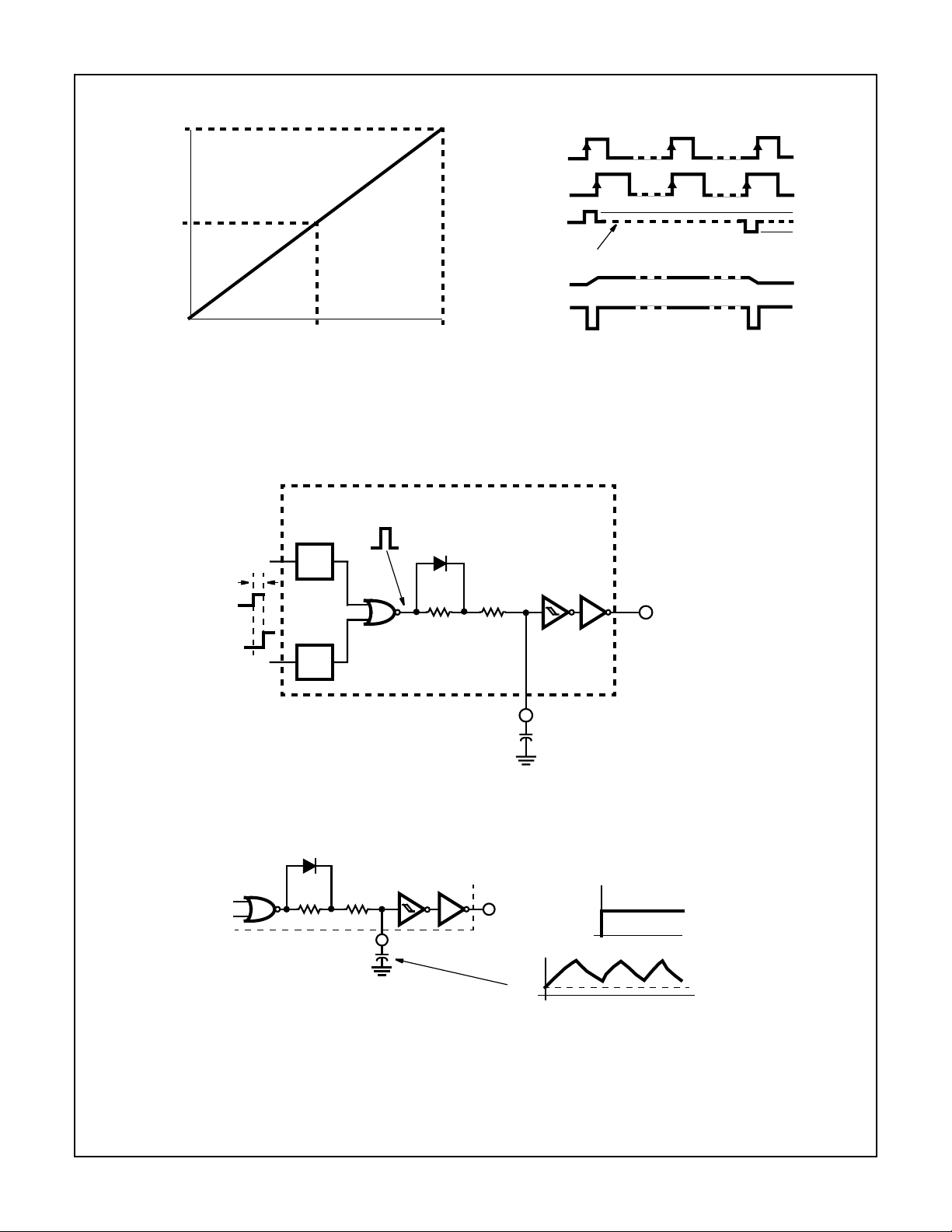
Lock Detector Theory of Operation
Detection of a locked condition is accomplished by a NOR
gate and an envelope detector as shown in Figure 6. When
the PLL is in Lock, the output of the NOR gate is High and
the lock detector output (Pin 1) is at a constant high level. As
the loop tracks the signal on Pin 14 (signal in), the NOR gate
outputs pulses whose widths represent the phase differences between the VCO and the input signal. The time
between pulses will be approximately equal to the time constant of the VCO center frequency. During the rise time of
the pulse, the diode across the 1.5kΩ resistor is forward
biased and the time constant in the path that charges the
lock detector capacitor is T = (150Ω x C
LD
).
During the fall time of the pulse the capacitor discharges
through the 1.5kΩ and the 150Ω resistors and the channel
resistance of the n-device of the NOR gate to ground
(T = (1.5kΩ + 150Ω + Rn-channel) x C
LD
).
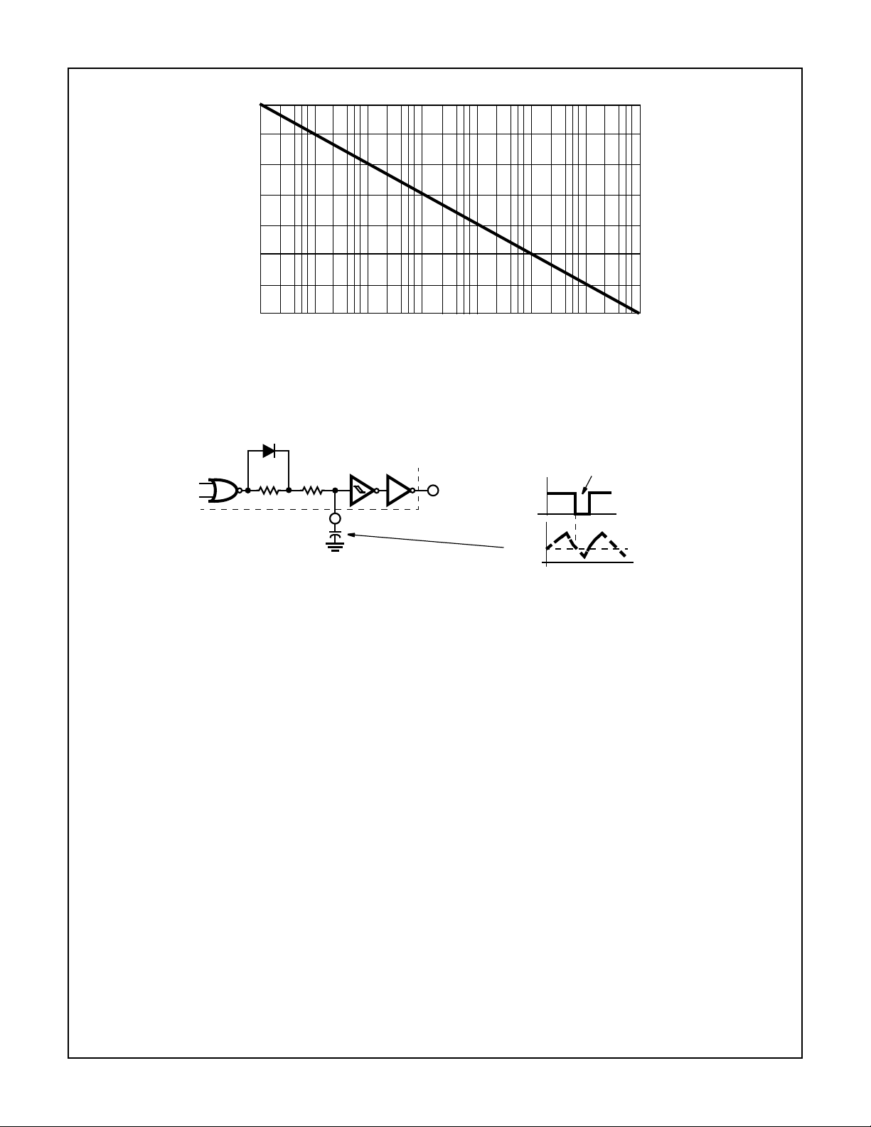
The waveform preset at the capacitor resembles a sawtooth
as shown in Figure 7. The lock detector capacitor value is
determined by the VCO center frequency. The typical range
of capacitor for a frequency of 10MHz is about 10pF and for
a frequency of 100kHz is about 1000pF. The chart in Figure
8 can be used to select the proper lock detector capacitor
value. As long as the loop remains locked and tracking, the
level of the sawtooth will not go below the switching threshold of the Schmitt-trigger inverter. If the loop breaks lock, the
width of the error pulse will be wide enough to allow the sawtooth waveform to go below threshold and a level change at
the output of the Schmitt trigger will indicate a loss of lock,
as shown in Figure 9. The lock detector capacitor also acts
to filter out small glitches that can occur when the loop is
either seeking or losing lock.
Note: When using phase comparator 1, the detector will only
indicate a lock condition on the fundamental frequency and
not on the harmonics, which PC1 will also lock on. If a detection of lock is needed over the harmonic locking range of
PC1, then the lock detector output must be OR-ed with the
output of PC1.
V
CC
V
DEMOUT (AV)
1/2 V
CC
0
o
0
FIGURE 2. PHASE COMPARATOR 1: AVERAGE OUTPUT
VOLTAGE vs INPUT PHASE DIFFERENCE:
V
DEMOUT
PIN
); φ
= V
DEMOUT
PC1OUT
= (φ
o
90
= (VCC/π) (φ
- φ
SIGIN
φ
DEMOUT
COMPIN
SIGIN
)
- φ
COM-
180
SIG
IN
COMP
IN
VCO
OUT
PC1
OUT
VCO
IN
o
FIGURE 3. TYPICAL WAVEFORMS FOR PLL USING PHASE
COMPARATOR 1, LOOP LOCKED AT f
V
CC
GND
o
4
V
DEMOUT (AV)
1/2 V
CD74HC7046A, CD74HCT7046A
V
CC
SIG
IN
COMP
IN
VCO
OUT
V
CC
PC2
VCO
OUT
HIGH IMPEDANCE OFF - STATE
IN
CC
GND
0
-360
o
o
φ
0
DEMOUT
FIGURE 4. PHASE COMPARATOR 2: AVERAGE OUTPUT
VOLTAGE vs INPUT PHASE DIFFERENCE:
V
DEMOUT
PIN
); φ
= V
DEMOUT
COMP
PC2OUT
= (φ
SIG
IN
IN
= (VCC/π) (φ
- φ
SIGIN
UP
FF
DN
FF
- φ
SIGIN
COMPIN
7046 LOCK DETECTOR CIRCUITRY
COM-
)
PHASE DIFFERENCE
o
360
1.5kΩ 150Ω
PIN 15
PCP
OUT
FIGURE 5. TYPICAL WAVEFORMS FOR PLL USING PHASE
COMPARATOR 2, LOOP LOCKED AT f
PIN 1
LOCK DETECTOR
OUTPUT
C
LD
LOCK DETECTOR
CAPACITOR
o
FIGURE 6. CD74HC/HCT7046A LOCK DETECTOR CIRCUIT
1.5kΩ 150Ω
PIN 15
LOCK
DETECTOR
CAPACITOR
PIN 1
C
LD
V
DETECTOR
CAP
LOCK
OUTPUT
V
TH
FIGURE 7. WAVEFORM PRESENT AT LOCK DETECTOR CAPACITOR WHEN IN LOCK
5
CD74HC7046A, CD74HCT7046A
10M
1M
100K
10K
1K
100
10
LOCK DETECTOR CAPACITOR VALUE (pF)
10 100 1K 10K 100K 1M 10M 100M
f, VCO CENTER FREQUENCY (HZ)
FIGURE 8. LOCK DETECTOR CAPACITOR SELECTION CHART
LOSS OF LOCK
1.5kΩ 150Ω
PIN 15
LOCK
DETECTOR
CAPACITOR
PIN 1
C
LD
LOCK
DETECTOR
OUTPUT
V
CAP
V
TH
FIGURE 9. WAVEFORM PRESENT AT LOCK DETECTOR CAPACITOR WHEN UNLOCKED
6
CD74HC7046A, CD74HCT7046A
Absolute Maximum Ratings Thermal Information
DC Supply Voltage, VCC. . . . . . . . . . . . . . . . . . . . . . . . -0.5V to 7V
DC Input Diode Current, I
IK
For VI < -0.5V or VI > VCC + 0.5V. . . . . . . . . . . . . . . . . . . . . .±20mA
DC Output Diode Current, I
OK
For VO < -0.5V or VO > VCC + 0.5V . . . . . . . . . . . . . . . . . . . .±20mA
DC Output Source or Sink Current per Output Pin, I
O
For VO > -0.5V or VO < VCC + 0.5V . . . . . . . . . . . . . . . . . . . .±25mA
DC VCC or Ground Current, ICC . . . . . . . . . . . . . . . . . . . . . . . . .±50mA
Operating Conditions
Temperature Range, TA . . . . . . . . . . . . . . . . . . . . . . -55oC to 125oC
Supply Voltage Range, V
HC Types . . . . . . . . . . . . . . . . . . . . . . . . . . . . . . . . . . . . .2V to 6V
HCT Types . . . . . . . . . . . . . . . . . . . . . . . . . . . . . . . . .4.5V to 5.5V
DC Input or Output Voltage, VI, VO . . . . . . . . . . . . . . . . . 0V to V
Input Rise and Fall Time
2V . . . . . . . . . . . . . . . . . . . . . . . . . . . . . . . . . . . . . . 1000ns (Max)
4.5V. . . . . . . . . . . . . . . . . . . . . . . . . . . . . . . . . . . . . . 500ns (Max)
6V . . . . . . . . . . . . . . . . . . . . . . . . . . . . . . . . . . . . . . . 400ns (Max)
CAUTION: Stresses above those listed in “Absolute Maximum Ratings” may cause permanent damage to the device. This is a stress only rating and operation
of the device at these or any other conditions above those indicated in the operational sections of this specification is not implied.
NOTE:
3. θJA is measured with the component mounted on an evaluation PC board in free air.
CC
Thermal Resistance (Typical, Note 3) θJA (oC/W)
PDIP Package. . . . . . . . . . . . . . . . . . . . . . . . . . . . . 90
SOIC Package. . . . . . . . . . . . . . . . . . . . . . . . . . . . . 160
Maximum Junction Temperature. . . . . . . . . . . . . . . . . . . . . . . 150oC
Maximum Storage Temperature Range . . . . . . . . . .-65oC to 150oC
Maximum Lead Temperature (Soldering 10s). . . . . . . . . . . . . 300oC
(SOIC - Lead Tips Only)
CC
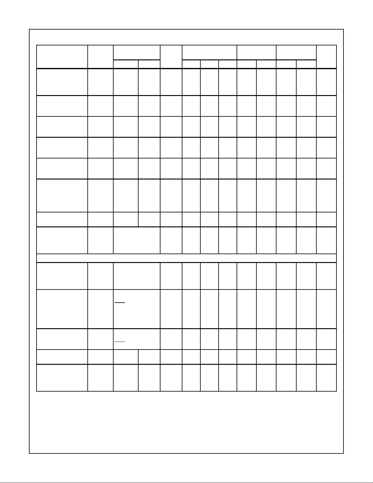
DC Electrical Specifications
PARAMETER SYMBOL
HC TYPES
VCO SECTION
INH High Level Input
Voltage
INH Low Level Input
Voltage
VCO
High Level
OUT
Output Voltage
CMOS Loads
VCO
High Level
OUT
Output Voltage
TTL Loads
VCO
OUT
Low Level
Output Voltage
CMOS Loads
VCO
OUT
Low Level
Output Voltage
TTL Loads
C1A, C1B Low Level
Output Voltage
(Test Purposes Only)
V
IH
V
IL
V
OH
V
OL
V
OL
TEST
CONDITIONS
(V) IO(mA) MIN TYP MAX MIN MAX MIN MAX
I
V
CC
(V)
o
C -40oC TO 85oC -55oCTO125oC
25
UNITSV
- - 3 2.1 - - 2.1 - 2.1 - V
4.5 3.15 - - 3.15 - 3.15 - V
6 4.2 - - 4.2 - 4.2 - V
- - 3 - - 0.9 - 0.9 - 0.9 V
4.5 - - 1.35 - 1.35 - 1.35 V
6 - - 1.8 - 1.8 - 1.8 V
VIHor VIL-0.02 3 2.9 - - 2.9 - 2.9 - V
-0.02 4.5 4.4 - - 4.4 - 4.4 - V
-0.02 6 5.9 - - 5.9 - 5.9 - V
- - ---- - - - V
-4 4.5 3.98 - - 3.84 - 3.7 - V
-5.2 6 5.48 - - 5.34 - 5.2 - V
VIHor VIL0.02 2 - - 0.1 - 0.1 - 0.1 V
0.02 4.5 - - 0.1 - 0.1 - 0.1 V
0.02 6 - - 0.1 - 0.1 - 0.1 V
- - ---- - - - V
4 4.5 - - 0.26 - 0.33 - 0.4 V
5.2 6 - - 0.26 - 0.33 - 0.4 V
VIL or
V
OL
4 4.5 - - 0.40 - 0.47 - 0.54 V
5.2 6 - - 0.40 - 0.47 - 0.54 V
7
CD74HC7046A, CD74HCT7046A
DC Electrical Specifications (Continued)
TEST
PARAMETER SYMBOL
INH VCOIN Input
Leakage Current
CONDITIONS
(V) IO(mA) MIN TYP MAX MIN MAX MIN MAX
I
I
VCC or
I
GND
V
CC
(V)
-6--±0.1 - ±1-±1µA
R1 Range (Note 4) - - - 4.5 3 - - - - - - kΩ
R2 Range (Note 4) - - - 4.5 3 - - - - - - kΩ
C1 Capacitance
Range
---3--No
4.5 40 - - - - - pF
6-- ----pF
VCO
Operating
IN
Voltage Range
- Over the range
specified for R1 for
LinearitySeeFigure
8, and 35 - 38
3 1.1 - 1.9 - - - - V
4.5 1.1 - 3.2 - - - - V
6 1.1 - 4.6 - - - - V
(Note 5)
PHASE COMPARATOR SECTION
SIG
, COMP
IN
IN
DC Coupled
High-Level Input
Voltage
SIG
, COMP
IN
IN
DC Coupled
Low-Level Input
Voltage
LD, PCn
OUT
HighLevel Output Voltage
CMOS Loads
V
IH
- - 2 1.5 - - 1.5 - 1.5 - V
4.5 3.15 - - 3.15 - 3.15 - V
6 4.2 - - 4.2 - 4.2 - V
V
IL
- - 2 - - 0.5 - 0.5 - 0.5 V
4.5 - - 1.35 - 1.35 - 1.35 V
6 - - 1.8 - 1.8 - 1.8 V
V
OH
VILor V
-0.02 2 1.9 - - 1.9 - 1.9 - V
IH
4.5 4.4 - - 4.4 - 4.4 - V
6 5.9 - - 5.9 - 5.9 - V
LD, PCn
Level Output Voltage
TTL Loads
LD, PCn
Level Output Voltage
CMOS Loads
OUT
OUT
High-
Low-
V
OH
VILor V
-4 4.5 3.98 - - 3.84 - 3.7 - V
IH
-5.2 6 5.48 - - 5.34 - 5.2 - V
V
OL
VILor V
0.02 2 - - 0.1 - 0.1 - 0.1 V
IH
4.5 - - 0.1 - 0.1 - 0.1 V
6 - - 0.1 - 0.1 - 0.1 V
LD, PCn
Level Output Voltage
TTL Loads
SIG
IN
Leakage Current
Low-
OUT
, COMPINInput
V
OL
VILor V
4 4.5 - - 0.26 - 0.33 - 0.4 V
IH
5.2 6 - - 0.26 - 0.33 - 0.4 V
I
VCC or
I
GND
-2--±3-±4-±5µA
3--±7-±9-±11 µA
4.5 - - ±18 - ±23 - ±29 µA
6--±30 - ±38 - ±45 µA
PC2
Three-State
OUT
I
OZ
VILor V
-6--±0.5 - ±5-±10 µA
IH
Off-State Current
SIG
, COMPINInput
IN
Resistance
R
I
VI at Self-Bias
Operation Point:
∆VI = 0.5V,
See Figure 8
3 - 800 - - - - - kΩ
4.5 - 250 - - - - - kΩ
6 - 150 - - - - - kΩ
DEMODULATOR SECTION
Resistor Range R
S
at RS > 300kΩ
Leakage Current
Can Influence
V
DEMOUT
3 10 - 300 - - - - kΩ
4.5 10 - 300 - - - - kΩ
6 10 - 300 - - - - kΩ
o
C -40oC TO 85oC -55oCTO125oC
25
----pF
Limit
UNITSV
8

CD74HC7046A, CD74HCT7046A
DC Electrical Specifications (Continued)
TEST
PARAMETER SYMBOL
OffsetVoltage VCO
to V
DEM
IN
V
OFF
CONDITIONS
(V) IO(mA) MIN TYP MAX MIN MAX MIN MAX
I
VI = V
V
VCOIN
CC
2
Values tak en over
V
CC
(V)
=
3-±30 - - - - - mV
4.5 - ±20 - - - - - mV
6-±10 - - - - - mV
RS Range
See Figure 15
Dynamic Output
Resistance at
DEM
OUT
Quiescent Device
Current
I
R
CC
V
CC
V
DEMOUT
O
2
=3-25-----Ω
4.5 - 25 - - - - - Ω
6 - 25 - - - - - Ω
Pins 3, 5 and 14
6 - - 8 - 80 - 160 µA
at VCC Pin 9 at
GND, II at Pins 3
and 14 to be
excluded
HCT TYPES
VCO SECTION
INH High Level Input
Voltage
INH Low Level Input
Voltage
VCO
High Level
OUT
V
IH
- - 4.5 to
2--2- 2 - V
5.5
V
IL
- - 4.5 to
- - 0.8 - 0.8 - 0.8 V
5.5
V
VIHor VIL-0.02 4.5 4.4 - - 4.4 - 4.4 - V
OH
Output Voltage
CMOS Loads
VCO
High Level
OUT
-4 4.5 3.98 - - 3.84 - 3.7 - V
Output Voltage
TTL Loads
VCO
OUT
Low Level
V
VIHor VIL0.02 4.5 - - 0.1 - 0.1 - 0.1 V
OL
Output Voltage
CMOS Loads
VCO
OUT
Low Level
4 4.5 - - 0.26 - 0.33 - 0.4 V
Output Voltage
TTL Loads
C1A, C1B Low Level
Output Voltage
V
OL
VIHor V
4 4.5 - - 0.40 - 0.47 - 0.54 V
IL
(Test Purposes Only)
INH VCO
Leakage Current
IN
Input
I
I
Any Voltage
Between VCC and
5.5 - ±0.1 - ±1-±1µA
GND
R1 Range (Note 4) - - - 4.5 3 - - - - - - kΩ
R2 Range (Note 4) - - - 4.5 3 - - - - - - kΩ
C1 Capacitance
- - - 4.5 40 - No
Range
VCO
Operating
IN
Voltage Range
- Over the range
specified for R1 for
4.5 1.1 - 3.2 - - - - V
LinearitySeeFigure
8, and 35 - 38
(Note 5)
PHASE COMPARATOR SECTION
SIG
, COMP
IN
DC Coupled
IN
V
IH
- - 4.5 to
3.15 - - 3.15 - 3.15 - V
5.5
High-Level Input
Voltage
o
C -40oC TO 85oC -55oCTO125oC
25
----pF
Limit
UNITSV
9
CD74HC7046A, CD74HCT7046A
DC Electrical Specifications (Continued)
TEST
PARAMETER SYMBOL
SIGIN, COMP
IN
DC Coupled
CONDITIONS
(V) IO(mA) MIN TYP MAX MIN MAX MIN MAX
I
V
IL
- - 4.5 to
V
CC
(V)
- - 1.35 - 1.35 - 1.35 V
5.5
Low-Level Input
Voltage
LD, PCn
OUT
High-
V
OH
VILor V
- 4.5 4.4 - - 4.4 - 4.4 - V
IH
Level Output Voltage
CMOS Loads
LD, PCn
OUT
High-
V
OH
VILor V
- 4.5 3.98 - - 3.84 - 3.7 - V
IH
Level Output Voltage
TTL Loads
LD, PCn
OUT
Low-
V
OL
VILor V
- 4.5 - - 0.1 - 0.1 - 0.1 V
IH
Level Output Voltage
CMOS Loads
LD, PCn
OUT
Low-
V
OL
VILor V
- 4.5 - - 0.26 - 0.33 - 0.4 V
IH
Level Output Voltage
TTL Loads
SIG
, COMPINInput
IN
Leakage Current
I
I
Any
- 5.5 - - ±30 ±38 ±45 µA
Voltage
Between
VCCand
GND
PC2
Three-State
OUT
I
OZ
VILor V
- 5.5 - - ±0.5 ±5- -±10 µA
IH
Off-State Current
SIG
, COMPINInput
IN
Resistance
R
I
VI at Self-Bias
4.5 - 250 - - - - - kΩ
Operation Point:
∆V, 0.5V,
See Figure 8
DEMODULATOR SECTION
Resistor Range R
S
at RS > 300kΩ
4.5 10 - 300 - - - - kΩ
Leakage Current
Can Influence
V
DEMOUT
OffsetVoltage VCO
to V
DEM
V
IN
OFF
V
VI = V
CC
VCOIN
=
4.5 - ±20 - - - - - mV
2
Values tak en over
RS Range
See Figure 15
Dynamic Output
Resistance at
DEM
OUT
Quiescent Device
Current
Additional Quiescent
Device Current Per
Input Pin: 1 Unit Load
Note 6
R
O
V
CC
V
DEMOUT
= 4.5 - 25 - - - - - Ω
2
I
CC
VCC or
- 5.5 - - 8 - 80 - 160 µA
GND
∆I
CC
V
CC
-2.1
- 4.5 to
5.5
- 100 360 - 450 - 490 µA
(Exclud-
ing Pin 5)
NOTES:
4. The valuefor R1 andR2 inparallel should exceed2.7kΩ; R1and R2 valuesabove 300kΩmay contribute tofrequency shift due to leakage
currents.
5. The maximum operating voltage can be as high as V
-0.9V, however, this may result in an increased offset voltage.
CC
6. For dual-supply systems theoretical worst case (VI = 2.4V, VCC = 5.5V) specification is 1.8mA.
o
C -40oC TO 85oC -55oCTO125oC
25
UNITSV
10
CD74HC7046A, CD74HCT7046A
HCT Input Loading Table
INPUT UNIT LOADS
INH 1
NOTE: Unit Load is ∆ICClimit specified in DC Electrical Table, e.g.,
360µA max at 25oC.
Switching Specifications C
PARAMETER SYMBOL
HC TYPES
PHASE COMPARATOR SECTION
Propagation Delay t
SIGIN, COMPIN to PC
1OUT
Output Transition Time t
Output Enable Time, SIG
COMPIN to PC2
OUT
IN
Output Disable Time, SIG
COMPIN to PC2
OUT
ACCoupled Input Sensitivity (
) at SIGIN or COMP
P
IN
VCO SECTION
Frequency Stability with
Temperature Change
Maximum Frequency f
Center Frequency f
Frequency Linearity ∆f
PLH
THL
,
t
PZH
,
t
IN
PHZ
P-
= 50pF, Input tr, tf= 6ns
L
TEST
CONDITIONS VCC(V)
, t
PHL
, t
TLH
, t
PZL
, t
PLZ
V
I(P-P)
∆f
∆T
MAX
R1 = 100kΩ,
R2 = ∞
C1 = 50pF
R1 = 3.5kΩ
R2 = ∞
= 0pF
C
1
R1 = 9.1kΩ
R2 = ∞
o
C1 = 40pF
R1 = 3kΩ
R2 = ∞
VCOIN=VCC/2
VCO
R1 = 100kΩ
R2 = ∞
C1 = 100pF
25
o
C
-40oC TO
85oC
-55oC TO
125oC
UNITSMIN TYP MAX MIN MAX MIN MAX
2 - - 200 - 250 - 300 ns
4.5 - - 40 - 50 - 60 ns
6 - - 34 - 43 - 51 ns
2 - - 75 - 95 - 110 ns
4.5 - - 15 - 19 - 22 ns
6 - - 13 - 16 - 19 ns
2 - - 280 - 350 - 420 ns
4.5 - - 56 - 70 - 84 ns
6 - - 48 - 60 - 71 ns
2 - - 325 - 405 - 490 ns
4.5 - - 65 - 81 - 98 ns
6 - - 55 - 69 - 83 ns
3 - 11 - - - - - mV
4.5 - 15 - - - - - mV
6 - 33 - - - - - mV
3 - - - Typ 0.11 - - %/oC
o
4.5 - - - - - %/
6--- --%/
C
o
C
3 - - - - - - - MHz
4.5 - 24 - - - - - MHz
6 - - - - - - - MHz
3 - - - - - - - MHz
4.5 - 38 - - - - - MHz
6 - - - - - - - MHz
3 7 10 - - - - - MHz
4.5 12 17 - - - - - MHz
6 14 21 - - - - - MHz
3-------%
4.5 - 0.4 - - - - - %
6-------%
11

CD74HC7046A, CD74HCT7046A
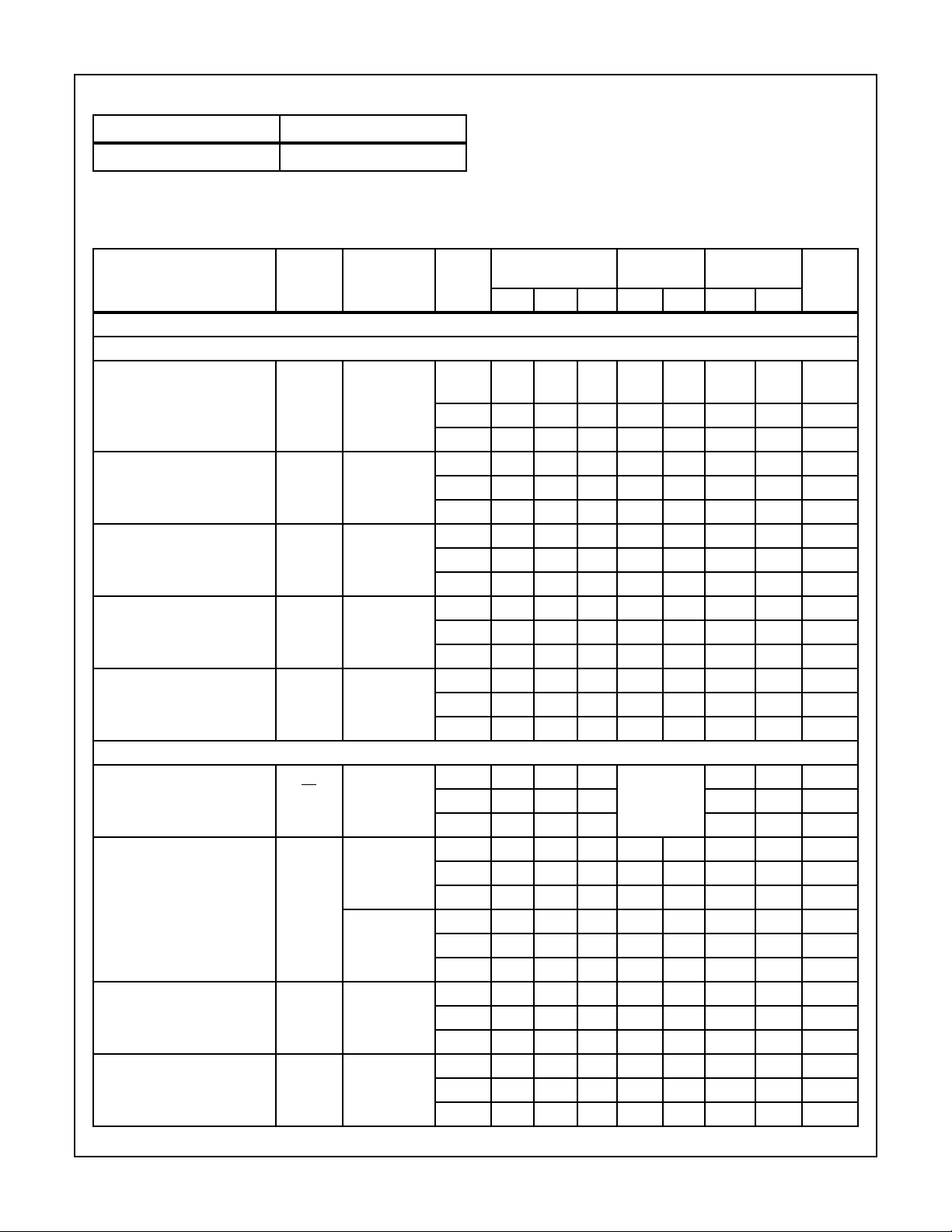
Switching Specifications C
= 50pF, Input tr, tf= 6ns (Continued)
L
TEST
PARAMETER SYMBOL
CONDITIONS VCC(V)
Offset Frequency R2 = 220kΩ
C1 = 1nF
DEMODULATOR SECTION
V
OUT
vs f
IN
R1 = 100kΩ
R2 = ∞
C1 = 100pF
R5 = 10kΩ
R3 = 100kΩ
C2 = 100pF
HCT TYPES
PHASE COMPARATOR SECTION
Propagation Delay t
SIGIN, COMPIN to PC
1OUT
Output Transition Time t
Output Enable Time, SIG
COMPIN to PC2
OUT
Output Disable Time, SIG
COMPIN to PCZ
OUT
,
IN
,
IN
AC Coupled Input Sensitivity
) at SIGIN or COMP
(
P-P
IN
PLH
THL
t
PZH
t
PHZ
, t
, t
, t
, t
PHL
TLH
PZL
PLZ
V
I(P-P)
VCO SECTION
Frequency Stability with
Temperature Change
Maximum Frequency f
∆f
∆T
MAX
R1 = 100kΩ,
R2 = ∞
C1 = 50pF
R1 = 3.5kΩ
R2 = ∞
= 0pF
C
1
R1 = 9.1kΩ
R2 = ∞
Center Frequency f
o
C1 = 40pF
R1 = 3kΩ
R2 = ∞
VCOIN=VCC/2
Frequency Linearity ∆f
VCO
R1 = 100kΩ
R2 = ∞
C1 = 100pF
Offset Frequency R
= 220kΩ
2
C1 = 1nF
DEMODULATOR SECTION
V
OUT
vs f
IN
R1 = 100kΩ
R2 = ∞
C1 = 100pF
R5 = 10kΩ
R3 = 100kΩ
C2 = 100pF
25
o
C
-40oC TO
85oC
-55oC TO
125oC
UNITSMIN TYP MAX MIN MAX MIN MAX
3 - - - - - - - kHz
4.5 - 400 - - - - - kHz
6 - - - - - - - kHz
3 - - - - - - - mV/kHz
4.5 - 330 - - - - - mV/kHz
6 - - - - - - - mV/kHz
4.5 - - 45 - 56 - 68 ns
4.5 - - 15 - 19 - 22 ns
4.5 - - 60 - 75 - 90 ns
4.5 - - 70 - 86 - 105 ns
3 - 11 - - - - - mV
4.5 - 15 - - - - - mV
6 - 33 - - - - - mV
4.5 - - - Typ 0.11 - - %/oC
4.5 - 24 - - - - - MHz
4.5 - 38 - - - - - MHz
4.5 12 17 - - - - - MHz
4.5 - 0.4 - - - - - %
4.5 - 400 - - - - - kHz
4.5 - 330 - - - - - mV/kHz
12

CD74HC7046A, CD74HCT7046A
Test Circuits and Waveforms
tr = 6ns tf = 6ns
INPUT
90%
50%
10%
V
CC
GND
tr = 6ns
INPUT
2.7V
1.3V
0.3V
= 6ns
t
f
3V
GND
t
THL
t
TLH
90%
t
50%
10%
PLH
INVERTING
OUTPUT
t
PHL
FIGURE 10. HC TRANSITION TIMES AND PROPAGATION
DELAY TIMES, COMBINATION LOGIC
Typical Performance Curves
I
I
∆V
I
SELF-BIAS OPERATING POINT
V
I
FIGURE 12. TYPICAL INPUT RESISTANCE CURVE AT
SIGIN, COMP
IN
t
THL
t
TLH
90%
t
PLH
1.3V
10%
INVERTING
OUTPUT
t
PHL
FIGURE 11. HCT TRANSITION TIMES AND PROPAGATION
DELAY TIMES, COMBINATION LOGIC
8
10
7
10
6
10
5
10
4
10
3
10
2
10
CENTER FREQUENCY (Hz)
VCOIN = 0.5 V
VCC= 4.5V
10
CC
R1 = 2.2K
R1 = 22K
R1 = 220K
R1 = 2.2M
R1 = 11M
R2 = ∞
1
110
2
10
3
10
4
10
5
10
6
10
CAPACITANCE, C1 (pF)
FIGURE 13. HC7046A TYPICAL CENTER FREQUENCY vs R1, C1
8
10
7
10
6
10
5
10
4
10
3
10
2
10
CENTER FREQUENCY (Hz)
10
1
110
VCOIN = 0.5 V
VCC= 6.0V
R2 = ∞
CC
2
10
3
10
10
4
R1 = 3K
R1 = 30K
R1 = 330K
R1 = 3M
R1 = 15M
5
10
6
10
CAPACITANCE, C1 (pF)
FIGURE 14. HC7046A TYPICAL CENTER FREQUENCY vs R1, C1
8
10
7
10
6
10
5
10
4
10
3
10
2
10
VCOIN = 0.5 V
CENTER FREQUENCY (Hz)
VCC= 3.0V
10
R2 =
1
110
CC
∞
2
10
3
10
10
4
R1 = 1.5K
R1 = 15K
R1 = 150K
R1 = 1.5M
R1 = 7.5M
5
10
CAPACITANCE, C1 (pF)
FIGURE 15. HC7046A TYPICAL CENTER FREQUENCY vs R1, C1
13
6
10

CD74HC7046A, CD74HCT7046A
Typical Performance Curves
8
10
7
10
6
10
5
10
4
10
3
10
2
10
CENTER FREQUENCY (Hz)
VCOIN = 0.5 V
VCC= 4.5V
10
R2 = ∞
1
110
CC
2
10
CAPACITANCE, C1 (pF)
3
10
(Continued)
R1 = 2.2K
R1 = 22K
R1 = 220K
R1 = 2.2M
R1 = 11M
4
10
8
10
7
10
6
10
5
10
4
10
3
10
2
10
VCOIN = 0.5 V
CENTER FREQUENCY (Hz)
VCC= 5.5V
10
R2 = ∞
5
10
6
10
1
110
CC
2
10
CAPACITANCE, C1 (pF)
3
10
10
4
R1 = 3K
R1 = 30K
R1 = 300K
R1 = 3M
R1 = 15M
5
10
6
10
FIGURE 16. HCT7046A TYPICAL CENTER FREQUENCY vs R1, C1 FIGURE17. HCT7046A TYPICAL CENTER FREQUENCY vs R1, C1
140
C1 = 50pF
R1 = 1.5M
120
R2 = ∞
100
80
60
VCO FREQUENCY (kHz)
40
20
01 2 3456
VCC = 3V
VCC = 4.5V
(V)
VCO
IN
VCC = 6V
FIGURE 18. HC7046A TYPICAL VCO FREQUENCY vs VCO
IN
90
C1 = 0.1µF
R1 = 1.5M
80
R2 = ∞
70
60
50
40
30
VCO FREQUENCY (Hz)
20
10
01 2 3 45 6
VCC = 3V
VCC = 4.5V
(V)
VCO
IN
VCC = 6V
FIGURE 19. HC7046A TYPICAL VCO FREQUENCY vs VCO
IN
(R1 = 1.5MΩ, C1 = 0.1µF)
800
C1 = 0.1µF
R1 = 150K
700
R2 = ∞
600
500
400
300
VCO FREQUENCY (Hz)
200
100
01 23 45 6
VCC = 3V
VCC = 4.5V
VCO
(V)
IN
VCC = 6V
FIGURE 20. HC7046A TYPICAL VCO FREQUENCY vs VCO
(R1 = 150kΩ, C1 = 0.1µF)
18
C1 = 0.1µF
16
R1 = 5.6k
R2 = ∞
14
12
10
8
6
VCO FREQUENCY (kHz)
4
2
01 23 45 6
IN
FIGURE 21. HC7046A TYPICAL VCO FREQUENCY vs VCO
VCC = 3V
VCO
VCC = 4.5V
(V)
IN
VCC = 6V
IN
(R1 = 5.6kΩ, C1 = 0.1µF)
14

CD74HC7046A, CD74HCT7046A
Typical Performance Curves
1400
C1 = 50pF
R1 = 150K
1200
1000
800
600
VCO FREQUENCY (kHz)
400
200
FIGURE 22. HC7046A TYPICAL VCO FREQUENCY vs VCO
∞
R2 =
VCC = 4.5V
VCC = 3V
01 23 45 6
VCO
IN
(Continued)
VCC = 6V
(V)
IN
(R1 = 150kΩ, C1 = 0.1µF)
24
VCOIN = 0.5 V
20
C1 = 50pF, VCC = 3V
R2 =
16
12
8
4
0
-4
-8
VCO FREQUENCY CHANGE, ∆f (%)
-12
-16
-75 -50 -25 0 25 50 75
CC
∞
AMBIENT TEMPERATURE, T
R1 = 1.5M
100 125 150
(oC)
A
R1 = 150K
R1 = 3K
FIGURE 24. HC7046A TYPICAL CHANGE IN VCO FREQUENCY
vs AMBIENT TEMPERATURE AS A FUNCTION OF
R1 (VCC = 3V)
24
C1 = 50pF
R1 = 5.6K
20
R2 = ∞
16
12
VCO FREQUENCY (MHz)
8
4
01 2 3 45 6
VCC = 3V
VCC = 4.5V
VCO
IN
(V)
FIGURE 23. HC7046A TYPICAL VCO FREQUENCY vs VCO
VCC = 6V
IN
(R1 = 5.6kΩ, C1 = 50pF)
VCOIN = 0.5 V
20
C1 = 50pF, VCC = 4.5V
16
R2 =
12
8
4
0
-4
-8
VCO FREQUENCY CHANGE, ∆f (%)
-12
-75 -50 -25 0 25 50 75
CC
∞
AMBIENT TEMPERATURE, TA (oC)
R1 = 2.2M
R1 = 220K
R1 = 2.2K
100 125 150
FIGURE25. HC7046A TYPICAL CHANGEIN VCO FREQUENCYvs
AMBIENT TEMPERA TURE AS A FUNCTION OF R1
15

CD74HC7046A, CD74HCT7046A
Typical Performance Curves
VCOIN = 0.5 V
16
C1 = 50pF, VCC = 6.0V
12
R2 =
8
CC
∞
(Continued)
R1 = 3M
R1 = 300K
4
0
-4
R1 = 3K
-8
VCO FREQUENCY CHANGE, ∆f (%)
-12
-75 -50 -25 0 25 50 75
AMBIENT TEMPERATURE, T
100 125 150
(oC)
A
FIGURE26. HC7046A TYPICAL CHANGEIN VCO FREQUENCYvs
AMBIENT TEMPERA TURE AS A FUNCTION OF R1
VCOIN = 0.5 V
20
C1 = 50pF, VCC = 4.5V
16
R2 =
CC
R1 = 2.2M
∞
12
8
R1 = 220K
4
0
VCO FREQUENCY CHANGE, ∆f (%)
-4
-8
R1 = 2.2K
-12
-75 -50 -25 0 25 50 75
AMBIENT TEMPERATURE, T
100 125 150
(oC)
A
FIGURE28. HC7046A TYPICAL CHANGEIN VCO FREQUENCYvs
AMBIENT TEMPERA TURE AS A FUNCTION OF R1
20
VCOIN = 0.5 V
C1 = 50pF, VCC = 5.5V
16
R2 =
CC
∞
R1 = 3M
12
8
R1 = 300K
4
0
R1 = 3K
VCO FREQUENCY CHANGE, ∆f (%)
-4
-8
-12
-75 -50 -25 0 25 50 75
AMBIENT TEMPERATURE, T
100 125 150
(oC)
A
FIGURE 27. HCT7046A TYPICAL CHANGE IN VCO
FREQUENCY vs AMBIENT TEMPERATURE AS A
FUNCTION OF R1
8
10
7
10
6
10
5
10
4
10
3
10
2
10
OFFSET FREQUENCY (Hz)
VCOIN = 0.5 V
10
VCC = 4.5V
1
110
CC
2
10
3
10
4
10
CAPACITANCE, C1 (pF)
FIGURE 29. HC7046A OFFSET FREQUENCY vs R2, C1
R2 = 2.2K
R2 = 22K
R2 = 220K
R2 = 2.2M
R2 = 11M
5
10
6
10
8
10
7
10
6
10
5
10
4
10
3
10
2
10
OFFSET FREQUENCY (Hz)
VCOIN = GND
10
V
1
110
CC
= 3V
2
10
3
10
10
CAPACITANCE, C1 (pF)
4
R2 = 1.5K
R2 = 15K
R2 = 150K
R2 = 1.5M
R2 = 7.5M
5
10
6
10
8
10
7
10
6
10
5
10
4
10
3
10
2
10
OFFSET FREQUENCY (Hz)
VCOIN = GND
10
V
1
110
CC
= 4.5V
2
10
3
10
10
CAPACITANCE, C1 (pF)
R2 = 2.2K
R2 = 22K
R2 = 220K
R2 = 2.2M
R2 = 11M
4
5
10
FIGURE 30. HC7046A OFFSET FREQUENCY vs R2, C1 FIGURE 31. HCT7046A OFFSET FREQUENCY vs R2, C1
16
6
10

CD74HC7046A, CD74HCT7046A
Typical Performance Curves
8
10
7
10
6
10
5
10
4
10
3
10
2
10
OFFSET FREQUENCY (Hz)
VCOIN = GND
= 6V
HC - V
10
1
CC
HCT - V
CC
= 5.5V
110
2
10
3
10
(Continued)
4
10
R2 = 3K
R2 = 30K
R2 = 300K
R2 = 3M
R2 = 15M
5
10
CAPACITANCE, C1 (pF)
FIGURE 32. HC7046A AND HCT7046A OFFSET FREQUENCY
vs R2, C1
VCOIN = VCC - 0.9V FOR f
2
VCOIN = 0V FOR f
10
VCC = 4.5V TO 5.5V
MAX
MIN
VCOIN = VCC - 0.9V FOR f
VCOIN = 0V FOR f
2
10
VCC = 3V, 4.5V, 6V
MIN
/f
10
MAX
f
6
10
1
-2
10
-1
10
MIN
MAX
1
10
2
10
R2/R1
FIGURE 33. HC7046A f
MIN/fMAX
vs R2/R1
f
MIN
/f
10
MAX
f
1
-2
10
FIGURE 34. HCT7046A f
8
C1 = 50pF
6
= 4.5V
V
CC
R2 =
4
2
0
-2
LINEARITY (%)
-4
-6
∞
-1
10
R2/R1
VCOIN = 2.25V ± 1V
1
MAX/fMIN
10
vs R2/R1 FIGURE 35. DEFINITION OF VCO FREQUENCY LINEARITY
VCOIN = 2.25V ± 0.45V
f
2
f
0
f
0’
f
1
∆V
2
10
MIN MAX
8
C1 = 50pF
V
= 3V
6
CC
∞
R2 =
1/2V
∆V
CC
∆V = 0.5V OVER THE VCC RANGE:
FOR VCO LINEARITY
= f1 + f
f’
o
2
2
- f
f’
o
o
LINEARITY =
V
VCOIN
x 100%
f’
o
4
2
VCOIN = 1.50V ± 0.4V
0
-2
LINEARITY (%)
VCOIN = 1.50V ± 0.3V
-4
-6
-8
1K 10K
100K 1M 10M
R1 (OHMS)
-8
1K 10K
100K 1M 10M
R1 (OHMS)
FIGURE 36. HC7046A VCO LINEARITY vs R1 FIGURE 37. HC7046A VCO LINEARITY vs R1
17

CD74HC7046A, CD74HCT7046A
Typical Performance Curves
8
C1 = 50pF
= 6V
V
6
CC
R2 =
∞
4
2
0
-2
LINEARITY (%)
-4
-6
-8
1K 10K
FIGURE 38. HC7046A VCO LINEARITY vs R1 FIGURE 39. HCT7046A VCO LINEARITY vs R1
4
10
(µW)
D
10
VCOIN = 0.5 V
3
CC
VCOIN = 3V ± 1.5V
100K 1M 10M
R1 (OHMS)
VCC = 6V
(Continued)
VCOIN = 3V ± 0.6V
8
VCC = 5.5V,
VCOIN = 2.75V ±1.3V
6
= 4.5V,
V
CC
VCO
IN
4
2
0
-2
LINEARITY (%)
-4
-6
-8
1K 10K
4
10
(µW)
VCOIN = 0.5 V
D
R1 = R2 = OPEN
3
10
= 2.25V ±1.0V
CC
VCC = 5.5V,
= 2.75V ±0.55V
VCO
IN
V
= 4.5V,
CC
VCO
= 2.25V ±0.45V
IN
100K 1M 10M
R1 (OHMS)
VCC = 6V
C1 = 50pF
R2 = OPEN
2
10
10
1
1K 10K
DEMODULATOR POWER DISSIPATION, P
VCC = 3V
RS (OHMS)
VCC = 4.5V
100K 1M
FIGURE 40. HC7046A DEMODULATOR POWER DISSIPATION
vs RS (TYP)
6
10
VCOIN = 0.5V
R2 = RS = OPEN
C
= 50pF
(µW)
D
VCO POWER DISSIPATION, P
L
5
10
4
10
VCC = 3V
C1 = 1µF
3
10
2
10
1K 10K
CC
VCC = 3V
C1 = 50pF
VCC = 6V
C1 = 50pF
VCC = 4.5V
C1 = 1µF
R1 (OHMS)
VCC = 6V
C1 = 1µF
100K 1M
VCC = 4.5V
C1 = 50pF
2
10
10
1
DEMODULATOR POWER DISSIPATION, P
1K 10K
VCC = 3V
100K 1M
RS (OHMS)
VCC = 4.5V
FIGURE 41. HCT7046A DEMODULATOR POWER DISSIPATION
vs RS (TYP) (VCC = 3V, 4.5V, 6V)
6
10
(µW)
D
5
10
4
10
3
10
VCO POWER DISSIPATION, P
2
10
VCC = 4.5V
1K 10K
VCC = 6V
C1 = 50pF
C1 = 1µF
VCC = 6V
C1 = 1µF
R2 (OHMS)
VCOIN = 0V (AT f
R1 = RS = ∞
CL = 50pF
VCC = 4.5V
C1 = 50pF
100K 1M
MIN
)
FIGURE 42. HC7046A VCO POWER DISSIPATION vs R1
(C1 = 50pF, 1µF)
FIGURE 43. HCT7046A VCO POWER DISSIPATION vs R2
(C1 = 50pF, 1µF)
18
CD74HC7046A, CD74HCT7046A
Typical Performance Curves
6
10
(µW)
D
5
10
4
10
VCC = 5.5V
C1 = 1µF
3
10
VCO POWER DISSIPATION, P
2
10
1K 10K
VCC = 5.5V
C1 = 50pF
VCC = 4.5V
C1 = 1µF
R1 (OHMS)
(Continued)
VCOIN = 0.5V
R2 = RS = ∞
VCC = 4.5V
C1 = 50pF
100K 1M
FIGURE 44. HCT7046A VCO POWER DISSIPATION vs R1
(C1 = 50pF, 1µF)
6
10
(µW)
D
5
10
4
10
VCC = 3V
C1 = 1µF
3
10
VCO POWER DISSIPATION, P
2
10
1K 10K
VCC = 6V
C1 = 50pF
VCC = 3V
C1 = 50pF
VCC = 4.5V
C1 = 1µF
R2 (OHMS)
VCOIN = 0V (AT f
R1 = RS = ∞
CL = 50pF
VCC = 4.5V
C1 = 50pF
100K 1M
MIN
VCC = 6V
C1 = 1µF
)
FIGURE 45. HC7046A VCO POWER DISSIPATION vs R2 (C1 =
50pF, 1µF)
19

CD74HC7046A, CD74HCT7046A
HC/HCT7046A C
PD
CHIP SECTION HC HCT UNIT
Comparator 1 48 50 pF
Comparator 2 39 48 pF
VCO 61 53 pF
Application Information
This information is a guide for the approximation of values of
external components to be used with the CD74HC7046A
and CD74HCT7046A in a phase-lock-loop system.
PHASE
SUBJECT
VCO Frequency
Without Extra Offset
(R2 = ∞)
COMPARATOR DESIGN CONSIDERATIONS
PC1 or PC2 VCO Frequency Characteristic
The characteristics of the VCO operation are shown in Figures 13 - 23.
f
f
References should be made to Figures 13 through 23 and
Figures 36 through 41 as indicated in the table.
Values of the selected components should be within the following ranges:
R1 > 3kΩ;
R2 > 3kΩ;
R1 || R2 parallel value > 2.7kΩ;
C1 greater than 40pF
MAX
VCO
f
o
2f
L
VCO Frequency with
Extra Offset
(R2 > 3kΩ)
f
MIN
MIN
FIGURE 46. FREQUENCY CHARACTERISTIC OF VCO OPERATING WITHOUT
OFFSET: fo = CENTER FREQUENCY: 2fL = FREQUENCY LOCK RANGE
PC1 Selection of R1 and C1
Given fo, determine the values of R1 and C1 using Figures 13 - 17.
PC2 Given f
To obtain 2fL: 2f
calculate foas f
MAX
MAX
2(∆VCOIN)
≈ where 0.9V < VCO
L
R1C1
PC1 or PC2 VCO Frequency Characteristic
The characteristics of the VCO operation are shown in Figures 29 - 32.
f
MAX
f
VCO
f
o
f
MIN
MIN
FIGURE 47. FREQUENCY CHARACTERISTIC OF VCO OPERATING WITH OFFSET:
= CENTER FREQUENCY: 2fL = FREQUENCY LOCK RANGE
f
o
V
1/2 V
CC
VCOIN
MAX
/2 and determine the values of R1 and C1 using Figures 13 - 17.
< VCC - 0.9V is the range of ∆VCO
1/2 V
CC
IN
2f
L
V
VCOIN
MAX
IN
PC1 or PC2 Selection of R1, R2 and C1
Given fo and fL, offset frequency, f
Obtain the values of C1 and R2 by using Figures 29 - 32.
Calculate the values of R1 from Figures 33 - 34.
20
, may be calculated from f
MIN
MIN
≈ f
- 1.6 fL.
o

SUBJECT
PLL Conditions with
No Signal at the
SIGIN Input
PLL Frequency
Capture Range
PHASE
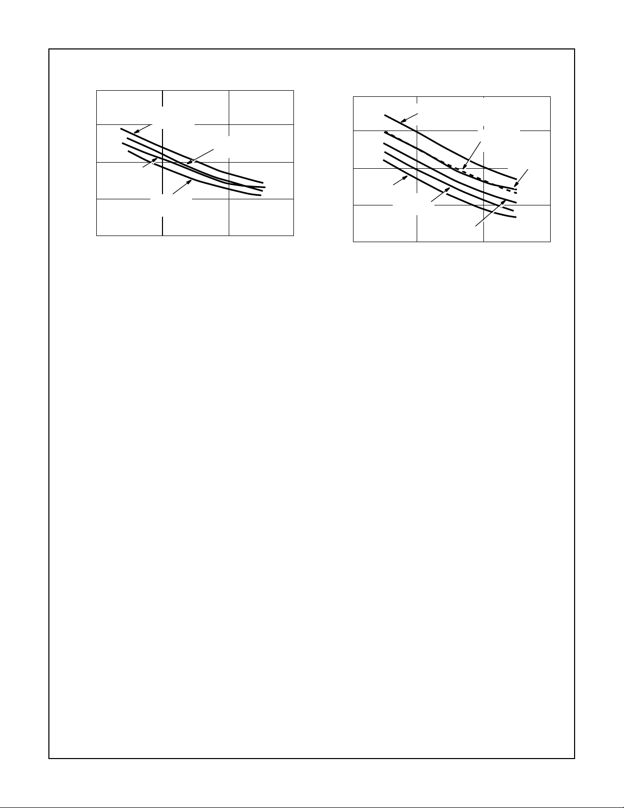
COMPARATOR DESIGN CONSIDERATIONS
PC1 VCO adjusts to fo with φ
PC2 VCO adjusts to f
MIN
with φ
DEMOUT
= 90o and V
DEMOUT
VCOIN
= -360o and V
= 1/2 VCC (see Figure 2)
= 0V (see Figure 4)
VCOIN
PC1 or PC2 Loop Filter Component Selection
|F
|
R3
C2
INPUT OUTPUT
(jω)
ω
(A) τ1 = R3 x C2
A small capture range (2fc) is obtained if τ > 2f
FIGURE 48. SIMPLE LOOP FILTER FOR PLL WITHOUT OFFSET
R3
INPUT OUTPUT
R4
C2
(A) τ2 = R4 x C2;
(B) AMPLITUDE CHARACTERISTIC (C) POLE-ZERO DIAGRAM
≈ (1/π) (2πf
c
|F
|
(jω)
m
1/
(B) AMPLITUDE CHARACTERISTIC (C) POLE-ZERO DIAGRAM
m =
R3 + R4
1/
3
τ
ω
2
τ
τ3 = (R3 + R4) x C2
L
R4
/τ1.)
1/2
-1/
-1/
τ
-1/
2
3
τ
τ
FIGURE 49. SIMPLE LOOP FILTER FOR PLL WITH OFFSET
PLL Locks on
Harmonics at Center
Frequency
Noise Rejection at
Signal Input
AC Ripple Content
when PLL is Locked
PC1 Yes
PC2 No
PC1 High
PC2 Low
PC1 fr = 2fi, large ripple content at φ
PC2 fr = fi, small ripple content at φ
Lock Detector Circuit
The lock detector feature is very useful in data synchronization, motor speed control, and demodulation. By adjusting
the value of the lock detector capacitor so that the lock output will change slightly before actually losing lock, the
designer can create an “early warning” indication allowing
corrective measures to be implemented. The reverse is also
true, especially with motor speed controls, generators, and
clutches that must be set up before actual lock occurs or disconnected during loss of lock.
When using phase comparator 1, the detector will only indicate a lock condition on the fundamental frequency and not
on the harmonics, which PC1 will lock on.
DEMOUT
DEMOUT
= 90
= 0
o
o
21

IMPORTANT NOTICE
T exas Instruments and its subsidiaries (TI) reserve the right to make changes to their products or to discontinue
any product or service without notice, and advise customers to obtain the latest version of relevant information
to verify, before placing orders, that information being relied on is current and complete. All products are sold
subject to the terms and conditions of sale supplied at the time of order acknowledgement, including those
pertaining to warranty, patent infringement, and limitation of liability.
TI warrants performance of its semiconductor products to the specifications applicable at the time of sale in
accordance with TI’s standard warranty. Testing and other quality control techniques are utilized to the extent
TI deems necessary to support this warranty . Specific testing of all parameters of each device is not necessarily
performed, except those mandated by government requirements.
CERT AIN APPLICATIONS USING SEMICONDUCTOR PRODUCTS MAY INVOLVE POTENTIAL RISKS OF
DEATH, PERSONAL INJURY, OR SEVERE PROPERTY OR ENVIRONMENTAL DAMAGE (“CRITICAL
APPLICATIONS”). TI SEMICONDUCTOR PRODUCTS ARE NOT DESIGNED, AUTHORIZED, OR
WARRANTED TO BE SUITABLE FOR USE IN LIFE-SUPPORT DEVICES OR SYSTEMS OR OTHER
CRITICAL APPLICA TIONS. INCLUSION OF TI PRODUCTS IN SUCH APPLICATIONS IS UNDERST OOD TO
BE FULLY AT THE CUSTOMER’S RISK.
In order to minimize risks associated with the customer’s applications, adequate design and operating
safeguards must be provided by the customer to minimize inherent or procedural hazards.
TI assumes no liability for applications assistance or customer product design. TI does not warrant or represent
that any license, either express or implied, is granted under any patent right, copyright, mask work right, or other
intellectual property right of TI covering or relating to any combination, machine, or process in which such
semiconductor products or services might be or are used. TI’s publication of information regarding any third
party’s products or services does not constitute TI’s approval, warranty or endorsement thereof.
Copyright 1999, Texas Instruments Incorporated
 Loading...