

Texas Instruments CD74HCT670M96, CD74HCT670M, CD74HCT670E, CD74HC670M96, CD74HC670M Datasheet
...
CD74HC670,
/
[ /Title
(CD74H
C670,
CD74H
CT670)
Subject
(HighSpeed
CMOS
Logic
4x4 Register
Data sheet acquired from Harris Semiconductor
SCHS195
January 1998
Features
• Simultaneous and Independent Read and Write
Operations
• Expandable to 512 Words of n-Bits
• Three-State Outputs
• Organized as 4 Words x 4 Bits Wide
• Buffered Inputs
• Typical Read Time = 16ns for CD74HC670 V
= 15pF, TA = 25oC
• Fanout (Over Temperature Range)
- Standard Outputs. . . . . . . . . . . . . . . 10 LSTTL Loads
- Bus Driver Outputs . . . . . . . . . . . . . 15 LSTTL Loads
• Wide Operating Temperature Range . . . -55
• Balanced Propagation Delay and Transition Times
• Significant Power Reduction Compared to LSTTL
Logic ICs
• HC Types
- 2V to 6V Operation
- High Noise Immunity: N
= 30%, NIH = 30% of V
IL
o
=5V,C
CC
C to 125oC
CC
CD74HCT670
High-Speed CMOS Logic
4x4 Register File
at VCC = 5V
• HCT Types
- 4.5V to 5.5V Operation
- Direct LSTTL Input Logic Compatibility,
V
= 0.8V (Max), VIH = 2V (Min)
IL
- CMOS Input Compatibility, I
Description
The Harris CD74HC670 and CD74HCT670 are 16-bit register
L
files organized as 4 words x 4 bits each. Read and write
address and enableinputs allow simultaneous writing into one
location while reading another. Four data inputs are provided
to store the 4-bit word. The write address inputs (WA0 and
WA1)determine the location of the stored word in the register.
When write enable (
address location and it remains transparent to the data. The
outputs will reflect the true form of the input data. When (
is high data and address inputs are inhibited. Data acquisition
from the four registers is made possible by the read address
inputs (RA1 and RA0). The addressed word appears at the
output when the read enable (
high impedance state when the (
tied together to increase the word capacity to 512 x 4 bits.
WE) is low the word is entered into the
Ordering Information
≤ 1µA at VOL, V
l
RE) is low. The output is in the
RE) is high. Outputs can be
OH
WE)
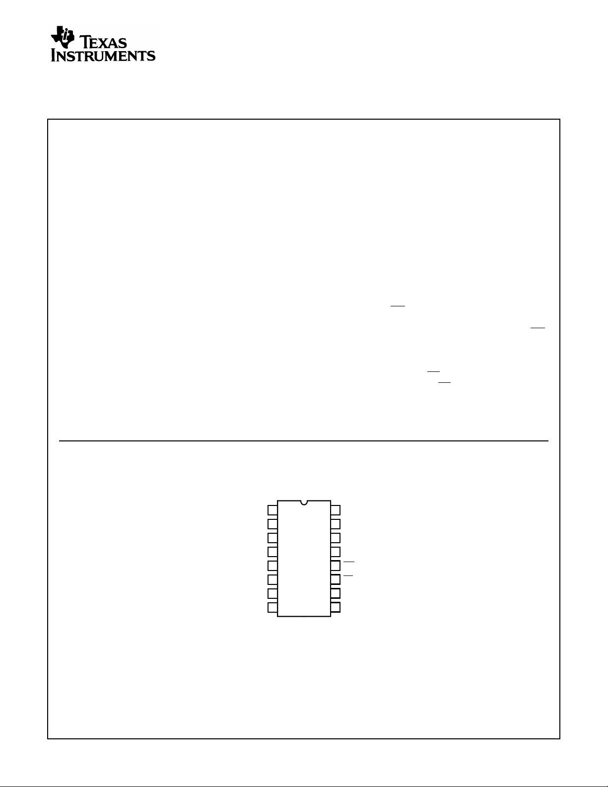
Pinout
CD74HC670, CD74HCT670
(PDIP, SOIC)
TOP VIEW
D1
D2
D3
RA1
RA0
Q3
Q2
GND
1
2
3
4
5
6
7
8
16
15
14
13
12
11
10
9
V
CC
D0
WA0
WA1
WE
RE
Q0
Q1
CAUTION: These devices are sensitive to electrostatic discharge. Users should follow proper IC Handling Procedures.
Copyright
© Harris Corporation 1998
1
File Number 1660.1
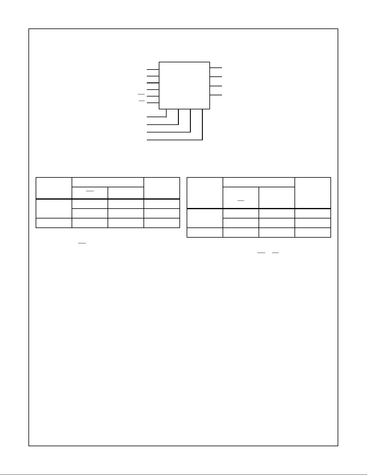
Functional Diagram
CD74HC670, CD74HCT670CD74HC670, CD74HCT670
15
D0
1
D1
2
D2
3
D3
12
WE
11
RE
RA1
RA0
WA0
WA1
4
WRITE MODE SELECT TABLE
INPUTS INTERNAL
OPERATING
MODE
N
LATCHES
(NOTE 3)WE D
Write Data L L L
LHH
Data Latched H X No Change
NOTE:
3. The WriteAddress (WA0 andWA1) to the“internal latches”must
be stable while WE is LOW for conventional operation.
10
Q0
9
Q1
7
Q2
6
Q3
514 13
READ MODE SELECT TABLE
INPUTS
INTERNAL
OPERATING
MODE
RE
LATCHES
(NOTE 4)
Read L L L
LHH
Disabled H X (Z)
NOTE:
4. The selectionof the “internal latches” byRead Address(RA0 and
RA1) are not constrained by WE or RE operation.
H = High Voltage Level
L = Low Voltage Level
X= Don’t Care
Z = High Impedance “Off” State
OUTPUT
Q
N
2
CD74HC670, CD74HCT670CD74HC670, CD74HCT670
Absolute Maximum Ratings Thermal Information
DC Supply Voltage, VCC. . . . . . . . . . . . . . . . . . . . . . . . -0.5V to 7V
DC Input Diode Current, I
IK
For VI < -0.5V or VI > VCC + 0.5V. . . . . . . . . . . . . . . . . . . . . .±20mA
DC Output Diode Current, I
OK
For VO < -0.5V or VO > VCC + 0.5V . . . . . . . . . . . . . . . . . . . .±20mA
DC Drain Current, per Output, I
O
For -0.5V < VO < VCC + 0.5V. . . . . . . . . . . . . . . . . . . . . . . . . .±35mA
DC Output Source or Sink Current per Output Pin, I
O
For VO > -0.5V or VO < VCC + 0.5V . . . . . . . . . . . . . . . . . . . .±25mA
DC VCC or Ground Current, ICC . . . . . . . . . . . . . . . . . . . . . . . . .±50mA
Operating Conditions
Temperature Range, TA . . . . . . . . . . . . . . . . . . . . . . -55oC to 125oC
Supply Voltage Range, V
HC Types . . . . . . . . . . . . . . . . . . . . . . . . . . . . . . . . . . . . .2V to 6V
HCT Types . . . . . . . . . . . . . . . . . . . . . . . . . . . . . . . . .4.5V to 5.5V
DC Input or Output Voltage, VI, VO . . . . . . . . . . . . . . . . . 0V to V
Input Rise and Fall Time
2V . . . . . . . . . . . . . . . . . . . . . . . . . . . . . . . . . . . . . . 1000ns (Max)
4.5V. . . . . . . . . . . . . . . . . . . . . . . . . . . . . . . . . . . . . . 500ns (Max)
6V . . . . . . . . . . . . . . . . . . . . . . . . . . . . . . . . . . . . . . . 400ns (Max)
CAUTION: Stresses above those listed in “Absolute Maximum Ratings” may cause permanent damage to the device. This is a stress only rating and operation
of the device at these or any other conditions above those indicated in the operational sections of this specification is not implied.
NOTE:
5. θJA is measured with the component mounted on an evaluation PC board in free air.
CC
Thermal Resistance (Typical, Note 5) θJA (oC/W)
PDIP Package. . . . . . . . . . . . . . . . . . . . . . . . . . . . . 90
SOIC Package. . . . . . . . . . . . . . . . . . . . . . . . . . . . . 160
Maximum Junction Temperature. . . . . . . . . . . . . . . . . . . . . . . 150oC
Maximum Storage Temperature Range . . . . . . . . . .-65oC to 150oC
Maximum Lead Temperature (Soldering 10s). . . . . . . . . . . . . 300oC
(SOIC - Lead Tips Only)
CC
DC Electrical Specifications
PARAMETER SYMBOL
HC TYPES
High Level Input
Voltage
Low Level Input
Voltage
High Level Output
Voltage
CMOS Loads
High Level Output
Voltage
TTL Loads
Low Level Output
Voltage
CMOS Loads
Low Level Output
Voltage
TTL Loads
Input Leakage
Current
V
IH
V
IL
V
OH
V
OL
I
I
TEST
CONDITIONS
(V) IO(mA) MIN TYP MAX MIN MAX MIN MAX
I
V
CC
(V)
o
C -40oC TO 85oC -55oCTO125oC
25
UNITSV
- - 2 1.5 - - 1.5 - 1.5 - V
4.5 3.15 - - 3.15 - 3.15 - V
6 4.2 - - 4.2 - 4.2 - V
- - 2 - - 0.5 - 0.5 - 0.5 V
4.5 - - 1.35 - 1.35 - 1.35 V
6 - - 1.8 - 1.8 - 1.8 V
VIHor VIL-0.02 2 1.9 - - 1.9 - 1.9 - V
-0.02 4.5 4.4 - - 4.4 - 4.4 - V
-0.02 6 5.9 - - 5.9 - 5.9 - V
- - ---- - - - V
-6 4.5 3.98 - - 3.84 - 3.7 - V
-7.8 6 5.48 - - 5.34 - 5.2 - V
VIHor VIL0.02 2 - - 0.1 - 0.1 - 0.1 V
0.02 4.5 - - 0.1 - 0.1 - 0.1 V
0.02 6 - - 0.1 - 0.1 - 0.1 V
- - ---- - - - V
6 4.5 - - 0.26 - 0.33 - 0.4 V
7.8 6 - - 0.26 - 0.33 - 0.4 V
VCC or
-6--±0.1 - ±1-±1µA
GND
3

CD74HC670, CD74HCT670CD74HC670, CD74HCT670
DC Electrical Specifications (Continued)
TEST
CONDITIONS
PARAMETER SYMBOL
Quiescent Device
I
CC
Current
Three-State Leakage
Current
HCT TYPES
High Level Input
Voltage
Low Level Input
Voltage
High Level Output
Voltage
V
IH
V
IL
V
OH
CMOS Loads
High Level Output
Voltage
TTL Loads
Low Level Output
Voltage
V
OL
CMOS Loads
Low Level Output
Voltage
TTL Loads
Input Leakage
Current
Quiescent Device
Current
I
I
I
CC
Three-State Leakage
Current
Additional Quiescent
Device Current Per
∆I
CC
Input Pin: 1 Unit Load
NOTE: For dual-supply systems theoretical worst case (V
(V) IO(mA) MIN TYP MAX MIN MAX MIN MAX
I
VCC or
0 6 - - 8 - 80 - 160 µA
GND
V
or VIHVO =
IL
VCC or
GND
- - 4.5 to
- - 4.5 to
VIHor VIL-0.02 4.5 4.4 - - 4.4 - 4.4 - V
-6 4.5 3.98 - - 3.84 - 3.7 - V
VIHor VIL0.02 4.5 - - 0.1 - 0.1 - 0.1 V
6 4.5 - - 0.26 - 0.33 - 0.4 V
VCCand
0 5.5 - ±0.1 - ±1-±1µA
GND
VCC or
0 5.5 - - 8 - 80 - 160 µA
GND
V
or VIHVO =
IL
VCC or
GND
V
CC
- 4.5 to
-2.1
o
C -40oC TO 85oC -55oCTO125oC
V
CC
25
(V)
6--±0.5 - ±5.0 - ±10 µA
2--2 - 2 - V
5.5
- - 0.8 - 0.8 - 0.8 V
5.5
5.5 - - ±0.5 - ±5.0 - ±10 µA
- 100 360 - 450 - 490 µA
5.5
= 2.4V, VCC = 5.5V) specification is 1.8mA.
I
UNITSV
HCT Input Loading Table
INPUT UNIT LOADS
WE 0.3
WA0 0.2
WA1 0.4
RE 1.5
DATA 0.15
RA0 0.4
RA1 0.7
NOTE: Unit load is ∆ICClimit specific in DC Electrical Specifications
Table, e.g., 360µA max. at 25oC.
4

CD74HC670, CD74HCT670CD74HC670, CD74HCT670
Prerequisite for Switching Specifications
25oC -40oC TO 85oC -55oC TO 125oC
PARAMETER SYMBOL VCC(V)
HC TYPES
Setup Time
tSU, t
h
Data to WE
Write to WE
Hold Time
tH, t
W
Data to WE
Write to WE
Pulse Width WE t
Latch Time WE to RA0,
W
t
LATCH
RA1
HCT TYPES
Setup Time
tSU, t
h
Data to WE
UNITSMIN TYP MAX MIN TYP MAX MIN TYP MAX
260--75- -90--ns
4.5 12 - - 15 - - 18 - - ns
610--13- -15--ns
25--5--5--ns
4.5 5 - - 5 - - 5 - - ns
65--5--5--ns
2 80 - - 100 - - 120 - - ns
4.5 16 - - 20 - - 24 - - ns
614- -17- -20- -ns
2 100 - - 125 - - 150 - - ns
4.5 20 - - 25 - - 30 - - ns
617- -21- -26- -ns
4.5 12 - - 15 - - 18 - - ns
Hold Time
tH, t
W
4.5 5 - - 5 - - 5 - - ns
Data to WE
Write to WE
Setup Time
t
SU
4.5 18 - - 23 - - 27 - - ns
Write to WE
Pulse Width WE t
Latch Time WE to RA0,
t
LATCH
W
4.5 20 - - 25 - - 30 - - ns
4.5 25 - - 31 - - 38 - - ns
RA1
Switching Specifications C
PARAMETER SYMBOL
= 50pF, Input tr, tf= 6ns
L
TEST
CONDITIONS VCC(V)
25
o
C
-40oC TO
85oC
-55oC TO
125oC
HC TYPES
Propagation Delay t
PLH
, t
PHLCL
= 50pF
Reading Any Word 2 - - 195 - 245 - 295 ns
4.5 - - 39 - 49 - 59 ns
CL = 15pF 5 - 16 - - - - - ns
= 50pF 6 - - 33 - 42 - 50 ns
C
L
Write Enable to Output t
PLH,tPHLCL
= 50pF 2 - - 250 - 315 - 375 ns
4.5 - - 50 - 63 - 75 ns
= 15pF 5 - 21 - - - - - ns
C
L
C
= 50pF 6 - - 43 - 54 - 64 ns
L
UNITSMIN TYP MAX MIN MAX MIN MAX
5

CD74HC670, CD74HCT670
Switching Specifications C
PARAMETER SYMBOL
Data to Output t
= 50pF, Input tr, tf= 6ns (Continued)
L
TEST
CONDITIONS VCC(V)
PLH,tPHLCL
= 50pF 2 - - 256 - 315 - 375 ns
25
o
C
-40oC TO
85oC
-55oC TO
125oC
4.5 - - 50 - 63 - 75 ns
= 15pF 5 - 21 - - - - - ns
C
L
C
= 50pF 6 - - 43 - 54 - 64 ns
L
Output Disable Time t
PLZ,tPHZ
CL = 50pF 2 - - 150 - 190 - 225 ns
4.5 - - 30 - 38 - 45 ns
CL = 15pF 5 - 12 - - - - - ns
= 50pF 6 - - 26 - 33 - 38 ns
C
L
Output Enable Time t
PZL,tPZH
CL = 50pF 2 - - 150 - 190 - 225 ns
4.5 - - 30 - 38 - 45 ns
CL = 15pF 5 - 12 - - - - - ns
= 50pF 6 - - 26 - 33 - 38 ns
C
L
Output Transition Time t
THL
, t
CL = 50pF 2 - - 75 - 95 - 110 ns
TLH
4.5 - - 15 - 19 - 22 ns
6 - - 13 - 10 - 19 ns
Input Capacitance C
Three-State Output
I
C
O
CL = 50pF - 10 - 10 - 10 - 10 pF
- - 20 - 20 - 20 - 20 pF
Capacitance
Power Dissipation Capacitance
C
PD
CL = 15pF 5 - 59 - - - - - pF
(Notes 6, 7)
HCT TYPES
Propagation Delay t
PHL,tPLH
Reading Any Word CL = 50pF 4.5 - - 40 - 50 - 53 ns
C
= 15pF 5 - 17 - - - - - ns
L
Write Enable to Output t
Data to Output t
Output Disable Time t
Output Enable Time t
Output Transition Time t
PHL,tPLH
PHL,tPLH
PLZ,tPHZ
PZL,tPZH
TLH
Input Capacitance C
Three-State Output
Capacitance
Power Dissipation Capacitance
C
, t
I
C
O
PD
CL = 50pF 4.5 - - 50 - 63 - 75 ns
= 15pF 5 - 21 - - - - - ns
C
L
CL = 50pF 4.5 - - 50 - 63 - 75 ns
= 15pF 5 - 21 - - - - - ns
C
L
CL = 50pF 4.5 - - 35 - 44 - 53 ns
= 15pF 5 - 14 - - - - - ns
C
L
CL = 50pF 4.5 - - 38 - 48 - 57 ns
= 15pF 5 - 16 - - - - - ns
C
L
CL = 50pF 4.5 - - 15 - 19 - 22 ns
THL
CL = 50pF - 10 - 10 - 10 - 10 pF
- - 20 - 20 - 20 - 20 pF
CL = 15pF 5 - 66 - - - - - pF
(Notes 6, 7)
NOTES:
is used to determine the dynamic power consumption, per output.
6. C
PD
7. PD=CPDV
CC
2
fi+ ∑ CLV
2
fOwhere fi= Input Frequency, fO= Output Frequency, CL= Output Load Capacitance, VCC= Supply
CC
Voltage.
UNITSMIN TYP MAX MIN MAX MIN MAX
6

Test Circuits and Waveforms
trC
L
CLOCK
10%
90%
50%
10%
tfC
t
L
WL
tWL+ tWH=
50%
t
CD74HC670, CD74HCT670CD74HC670, CD74HCT670
WH
fC
50%
I
L
V
CC
GND
t
rCL
CLOCK
= 6ns
0.3V
2.7V
1.3V
0.3V
t
fCL
t
WL
= 6ns
1.3V
t
WH
t
WL
+ tWH=
1.3V
I
fC
L
3V
GND
NOTE: Outputs should be switching from 10% VCC to 90% VCC in
accordance with devicetruthtable. For f
, input duty cycle = 50%.
MAX
FIGURE 1. HC CLOCK PULSE RISE AND FALL TIMES AND
PULSE WIDTH
tr = 6ns tf = 6ns
V
t
CC
GND
TLH
INPUT
t
THL
90%
50%
10%
90%
t
50%
10%
PLH
INVERTING
OUTPUT
t
PHL
FIGURE 3. HC TRANSITION TIMES AND PROPAGATION
DELAY TIMES, COMBINATION LOGIC
tfC
L
V
CC
50%
GND
t
H(L)
V
CC
50%
t
SU(L)
GND
CLOCK
INPUT
DAT A
INPUT
t
SU(H)
trC
L
90%
10%
t
H(H)
NOTE: Outputs should be switching from 10% VCC to 90% VCC in
accordance with devicetruthtable. For f
, input duty cycle = 50%.
MAX
FIGURE 2. HCT CLOCK PULSE RISE AND FALL TIMES AND
PULSE WIDTH
= 6ns
tr = 6ns
INPUT
t
2.7V
1.3V
0.3V
THL
t
f
3V
GND
t
TLH
90%
t
PLH
1.3V
10%
INVERTING
OUTPUT
t
PHL
FIGURE 4. HCT TRANSITION TIMES AND PROPAGATION
DELAY TIMES, COMBINATION LOGIC
CLOCK
INPUT
DAT A
INPUT
t
SU(H)
trC
L
2.7V
0.3V
t
H(H)
1.3V
1.3V
tfC
L
3V
1.3V
GND
t
H(L)
3V
1.3V
t
SU(L)
GND
OUTPUT
t
REM
V
CC
SET, RESET
OR PRESET
50%
90%
t
PLH
IC
t
TLH
t
THL
90%
50%
10%
t
PHL
GND
C
L
50pF
FIGURE 5. HC SETUP TIMES, HOLD TIMES, REMOVALTIME,
AND PROPAGATION DELAY TIMES FOR EDGE
TRIGGERED SEQUENTIAL LOGIC CIRCUITS
OUTPUT
t
REM
3V
SET, RESET
1.3V
90%
1.3V
t
t
PLH
TLH
90%
1.3V
10%
t
PHL
t
THL
OR PRESET
IC
C
L
50pF
FIGURE 6. HCT SETUP TIMES, HOLD TIMES, REMOVALTIME,
AND PROPAGATION DELAY TIMES FOR EDGE
TRIGGERED SEQUENTIAL LOGIC CIRCUITS
7
GND

CD74HC670, CD74HCT670CD74HC670, CD74HCT670
Test Circuits and Waveforms
6ns 6ns
OUTPUT
DISABLE
OUTPUT LOW
TO OFF
OUTPUT HIGH
TO OFF
50%
t
t
OUTPUTS
ENABLED
PLZ
PHZ
90%
10%
90%
OUTPUTS
DISABLED
(Continued)
10%
t
PZL
t
PZH
FIGURE 7. HC THREE-STATE PROPAGATION DELAY
WAVEFORM
OTHER
INPUTS
TIED HIGH
OR LOW
OUTPUT
DISABLE
50%
50%
OUTPUTS
ENABLED
IC WITH
THREE-
STATE
OUTPUT
V
CC
GND
OUTPUT
R
0.3
t
t
6ns
PZL
PZH
t
r
OUTPUT
DISABLE
OUTPUT LOW
TO OFF
OUTPUT HIGH
TO OFF
t
t
OUTPUTS
ENABLED
6ns t
PLZ
PHZ
10%
90%
f
2.7
1.3
OUTPUTS
DISABLED
FIGURE 8. HCT THREE-STATE PROPAGATION DELAY
WAVEFORM
= 1kΩ
L
C
L
50pF
VCC FOR t
GND FOR t
PLZ
PHZ
AND t
AND t
PZL
PZH
3V
GND
1.3V
1.3V
OUTPUTS
ENABLED
NOTE: Open drain waveforms t
VCC, CL = 50pF.
FIGURE 9. HC AND HCT THREE-STATE PROPAGATION DELAY TEST CIRCUIT
PLZ
and t
are the same as those for three-state shown on the left. The test circuit is Output RL=1kΩto
PZL
8

IMPORTANT NOTICE
T exas Instruments and its subsidiaries (TI) reserve the right to make changes to their products or to discontinue
any product or service without notice, and advise customers to obtain the latest version of relevant information
to verify, before placing orders, that information being relied on is current and complete. All products are sold
subject to the terms and conditions of sale supplied at the time of order acknowledgement, including those
pertaining to warranty, patent infringement, and limitation of liability.
TI warrants performance of its semiconductor products to the specifications applicable at the time of sale in
accordance with TI’s standard warranty. Testing and other quality control techniques are utilized to the extent
TI deems necessary to support this warranty . Specific testing of all parameters of each device is not necessarily
performed, except those mandated by government requirements.
CERT AIN APPLICATIONS USING SEMICONDUCTOR PRODUCTS MAY INVOLVE POTENTIAL RISKS OF
DEATH, PERSONAL INJURY, OR SEVERE PROPERTY OR ENVIRONMENTAL DAMAGE (“CRITICAL
APPLICATIONS”). TI SEMICONDUCTOR PRODUCTS ARE NOT DESIGNED, AUTHORIZED, OR
WARRANTED TO BE SUITABLE FOR USE IN LIFE-SUPPORT DEVICES OR SYSTEMS OR OTHER
CRITICAL APPLICA TIONS. INCLUSION OF TI PRODUCTS IN SUCH APPLICATIONS IS UNDERST OOD TO
BE FULLY AT THE CUSTOMER’S RISK.
In order to minimize risks associated with the customer’s applications, adequate design and operating
safeguards must be provided by the customer to minimize inherent or procedural hazards.
TI assumes no liability for applications assistance or customer product design. TI does not warrant or represent
that any license, either express or implied, is granted under any patent right, copyright, mask work right, or other
intellectual property right of TI covering or relating to any combination, machine, or process in which such
semiconductor products or services might be or are used. TI’s publication of information regarding any third
party’s products or services does not constitute TI’s approval, warranty or endorsement thereof.
Copyright 1999, Texas Instruments Incorporated
 Loading...