

Data sheet acquired from Harris Semiconductor
SCHS206
February 1998
CD74HC4059
High-Speed CMOS Logic
CMOS Programmable Divide-by-N Counter
[ /Title
(CD74
HC4059
)
/Subject
(HighSpeed
CMOS
Logic
CMOS
Pro-
Features
• Synchronous Programmable ÷N Counter N = 3 to 9999
or 15999
• Presettable Down-Counter
• Fully Static Operation
• Mode-Select Control of Initial Decade Counting
Function (÷10, 8, 5, 4, 2)
• Master Preset Initialization
• Latchable ÷N Output
• Fanout (Over Temperature Range)
- Standard Outputs. . . . . . . . . . . . . . . 10 LSTTL Loads
- Bus Driver Outputs . . . . . . . . . . . . . 15 LSTTL Loads
• Wide Operating Temperature Range . . . -55
• Balanced Propagation Delay and Transition Times
• Significant Power Reduction Compared to LSTTL
Logic ICs
• HC Types
- 2V to 6V Operation
- High Noise Immunity: N
at VCC = 5V
= 30%, NIH = 30% of V
IL
o
C to 125oC
CC
Description
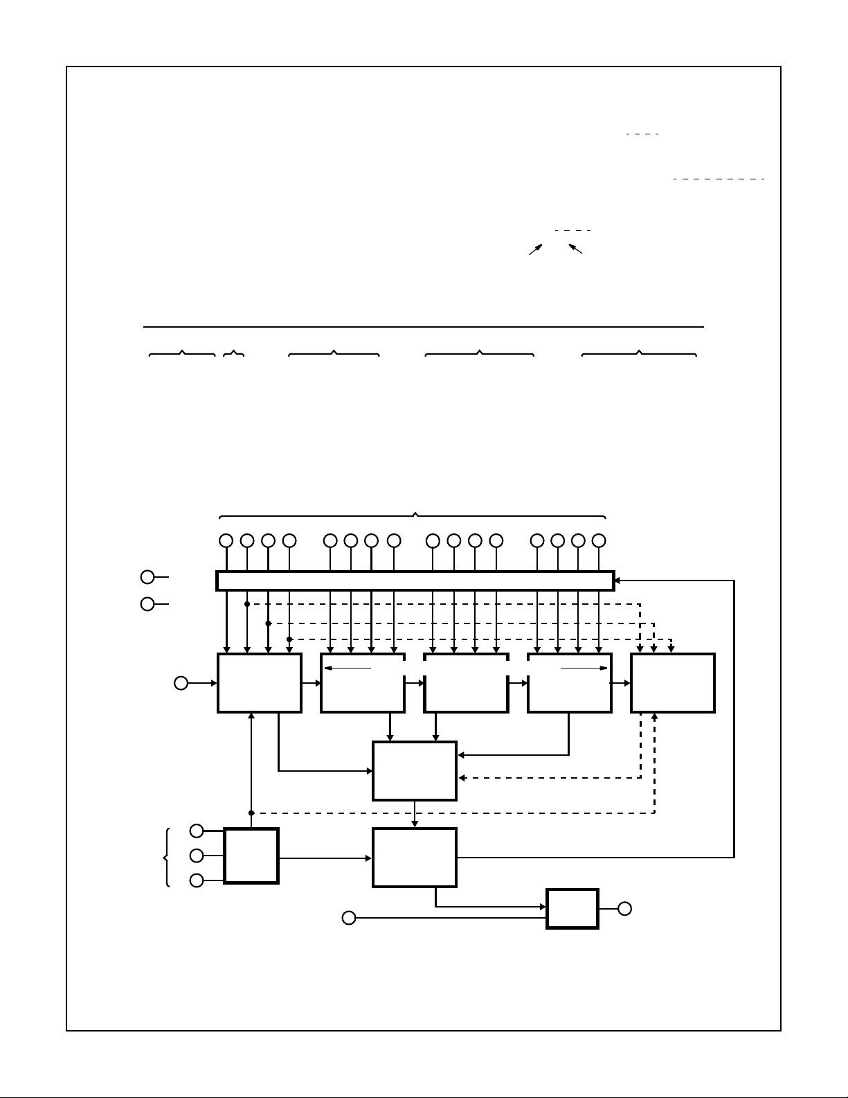
The Harris CD74HC4059 are high-speed silicon-gate
devices that are pin-compatible with the CD4059A devices of
the CD4000B series. These devices are divide-by-N downcounters that can be programmed to divide an input
frequency by any number “N” from 3 to 15,999. The output
signal is a pulse one clock cycle wide occurring at a rate
equal to the input frequency divide by N. The down-counter
is preset by means of 16 jam inputs.
The three Mode-Select Inputs K
modulus (“divide-by” number) of the first and last counting
sections in accordance with the truth table shown on Tab le 1.
Every time the first (fastest) counting section goes through one
cycle, it reduces by 1 the number that has been preset
(jammed) into the three decades of the intermediate counting
section an the last counting section, which consists of flip-flops
that are not needed for opening the first counting section. For
example, in the ÷2 mode, only one flip-flop is needed in the first
counting section. Therefore the last counting section has three
flip-flops that can be preset to a maximum count of seven with a
place value of thousands. If ÷10 is desired for the first section,
K
is set “high”, Kb“high” and Kc“low”. Jam inputs J1, J2, J3,
a
and J4 are used to preset the first counting section and there is
no last counting section. The intermediate counting section
consists of three cascaded BCD decade (÷10) counters
presettable by means of Jam Inputs J5 through J16.
and Kcdetermine the
a,Kb
Applications
• Communications Digital Frequency Synthesizers;
VHF, UHF, FM, AM, etc.
• Fixed or Programmable Frequency Division
• “Time Out” Timer for Consumer-Application Industrial
Controls
• AN6374 “Application of the CMOS CD4059A Programmable Divide-by-N Counter in FM and Citizens Band
Transceiver Digital Tuners”
Ordering Information
TEMP. RANGE
PART NUMBER
CD74HC4059E -55 to 125 24 Ld PDIP E24.3
NOTE:
1. Wafer and die is available which meets all electrical
specifications. Please contact your local sales office or Harris
customer service for ordering information.
(oC) PACKAGE
PKG.
NO.
The Mode-Select Inputs permit frequency-synthesizer
channel separations of 10, 12.5, 20, 25 or 50 parts. These
inputs set the maximum value of N at 9999 (when the first
counting section divides by 5 or 10) or 15,999 (when the first
counting section divides by 8, 4, or 2).
The three decades of the intermediate counter can be preset
to a binary 15 instead of a binary 9, while their place values
are still 1, 10, and 100, multiplied by the number of the ÷N
mode. For example, in the ÷8 mode, the number from which
counting down begins can be preset to:
3rd Decade 1500
2nd Decade 150
1st Decade 15
Last Counting Section 1000
The total of these numbers (2665) times 8 equals 12,320.
The first counting section can be preset to 7. Therefore,
21,327 is the maximum possible count in the ÷8 mode.
The highest count of the various is shown in the column entitled
Extended Counter Range of Table 1. Control inputs K
can be used to initiate and lock the counter in the “master
preset” state. In this condition the flip-flops in the counter are
preset in accordance with the jam inputs and the counter
remains in that state as long as K
counter begins to count down from the preset state when a
counting mode other than the master preset mode is selected.
and Kcboth remain low.The
b
and K
b
c
CAUTION: These devices are sensitive to electrostatic discharge. Users should follow proper IC Handling Procedures.
Copyright
© Harris Corporation 1998
1
File Number 1853.2
CD74HC4059CD74HC4059
The counter should always be put in the master preset mode
before the ÷5 mode is selected. Whenever the master preset
mode is used, control signals K
= “low” and Kc= “low” must
b
be applied for at least 3 full clock pulses.
After Preset Mode inputs have been changed to one of the ÷
modes, the next positive-going clock transition changes an
internal flip-flop so that the countdown can begin at the
second positive-going clock transition. Thus, after an MP
(Master Preset) mode, there is always one extra count
before the output goes high. Figure 1 illustrates a total count
of 3 (÷8 mode). If the Master Preset mode is started two
clock cycles or less before an output pules, the output pulse
will appear at the time due. If the Master Preset Mode is not
used, the counter jumps back to the “Jam” count when the
output pulse appears.
A “high” on the Latch Enable input will cause the counter
output to remain high once an output pulse occurs, and to
remain in the high state until the latch input returns to “low”.
If the Latch Enable is “low”, the output pulse will remain high
for only one cycle of the clock-input signal.
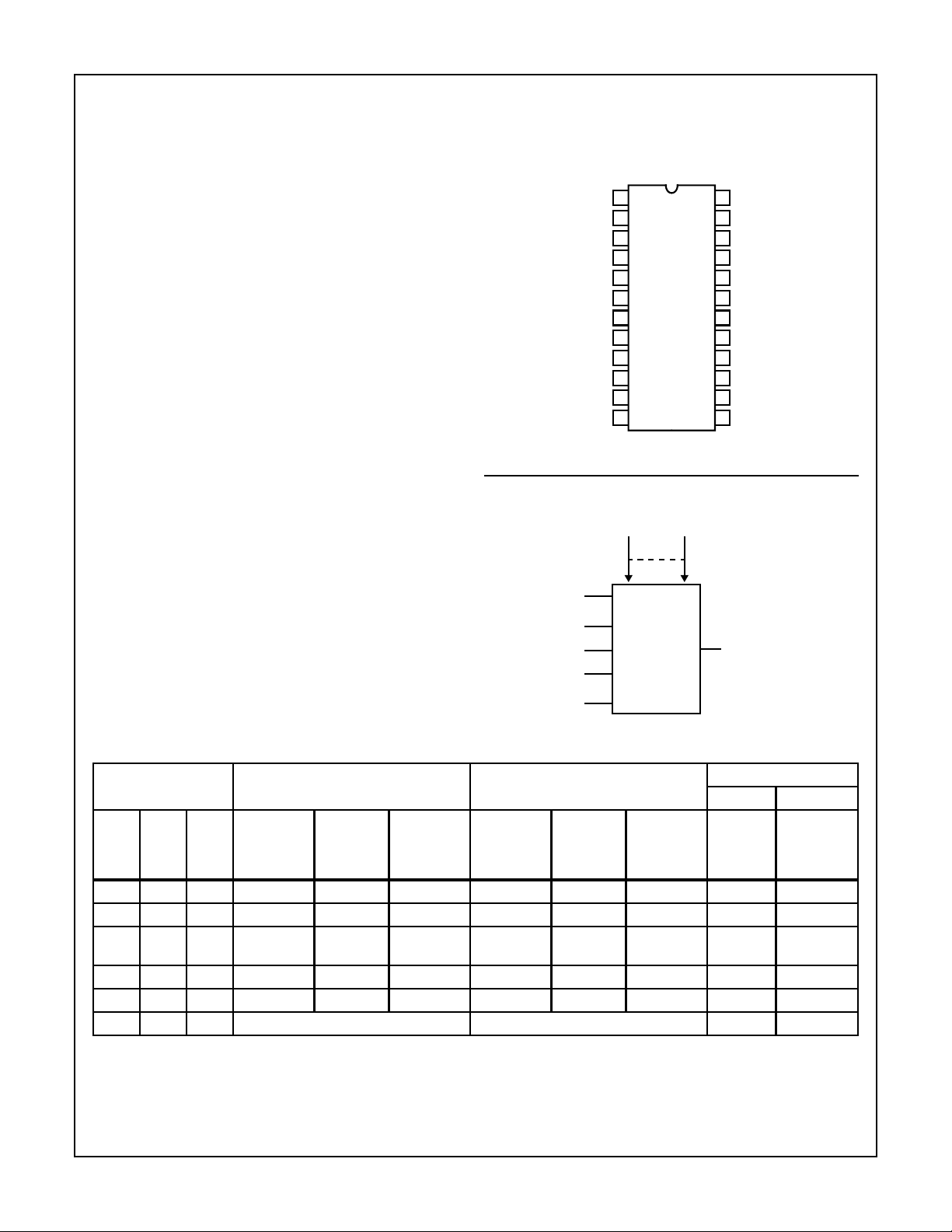
Pinout
CD74HC4059
TOP VIEW
CP
1
2
LE
J1
3
J2
4
J3
5
6
J4
J16
7
8
J15
J14
9
10
J13
K
11
c
12
GND
Functional Diagram
J1 - J16
(PDIP)
24
V
CC
23
Q
22
J5
21
J6
20
J7
19
J8
J9
18
17
J10
16
J11
15
J12
14
K
a
13
K
b
CP
K
K
K
LE
a
b
c
Q =
f
IN
-------
N
TRUTH TABLE
COUNTER RANGE
MODE SELECT INPUT FIRST COUNTING SECTION LAST COUNTING SECTION
CAN BE
PRESET
MODE
K
K
a
K
b
DIVIDES-BY
c
TO A MAX
OF:
(NOTE 3)
JAM
INPUTS
USED:
MODE
DIVIDES-BY
CAN BE
PRESET
TO A MAX
OF:
(NOTE 3)
JAM
INPUTS
USED: MAX MAX
DESIGN EXTENDED
H H H 2 1 J1 8 7 J2, J3, J4 15,999 17,331
L H H 4 3 J1, J2 4 3 J3, J4 15,999 18,663
HLH 5
4 J1, J2, J3 2 1 J4 9,999 13,329
(Note 4)
L L H 8 7 J1, J2, J3 2 1 J4 15,999 21,327
H H L 10 9 J1, J2, J3, J4 1 0 - 9,999 16,659
X L L Master Preset Master Preset - -
NOTES:
2. X = Don’t Care
3. J1 = Least Significant Bit. J4 = Most Significant Bit.
4. Operation in the ÷5 mode (1stcounting section) requires going through theMaster Preset mode prior to going into the ÷5 mode. At power
turn-on, Kc must be “low” for a period of 3 input clock pulses after VCC reaches a minimum of 3V.
2
CD74HC4059CD74HC4059
How to Preset the CD74HC/HCT4059 to Desired ÷N
The value N is determined as follows:
(EQ. 1)
N = (MODE†) (1000 x Decade 5 Preset + 100 x Decade 4
Preset + 10 x Decade 3 Preset + 1 x Decade 2 Preset) +
Decade 1 Preset
† MODE = First counting section divider (10, 8, 5, 4 or 2)
To calculate preset values for any N count, divide the N
count by the Mode. The resultant is the corresponding
preset values of the 5th through 2nd decade with the
remainder being equal to the 1st decade value.
Program Jam Inputs (BCD)
Example:
N = 8479, Mode = 5
Mode N
Preset Value =
N
Mode
1695 + 4 (Preset Values)
| 8479
5
(EQ. 2)
Mode Select = 5
K
aKbKc
HLH
41
J1 J2 J3 J4
L LH H
NOTE:
To verify the results, use Equation 1:
N = 5 (1000 x 1 + 100 x 6 + 10 x 9 + 1 x 5) + 4
N = 8479
J13J24J35J4
12
GND
24
V
CC
CLOCK
INPUT
1
FIRST
COUNTING
SECTION
÷10, 8, 5, 4, 2
J5 J6 J7 J8
H LHL
6
5
9
J9 J10 J11 J12
HLLH
PROGRAM JAM INPUTS (BCD)
J522J621J720J8
PRESETTABLE LOGIC
INTERMEDIATE COUNTING SECTION
÷10 ÷10 ÷10
J918J1017J1116J1215J1310J149J158J16
19
6
J13 J14 J15 J16
LHHL
7
P.E.
LAST
COUNTING
SECTION
÷1, 2, 2, 4, 8
MODE
SELECT
INPUTS
RECOGNITION
GATING
14
K
a
13
K
b
11
K
c
MODE
CONTROL
LATCH
ENABLE
PRESET
ENABLE
2
OUTPUT
STAGE
23
DIVIDE-BY-N
OUTPUT
FIGURE 1. FUNCTIONAL BLOCK DIAGRAM
3

CD74HC4059CD74HC4059
Absolute Maximum Ratings Thermal Information
DC Supply Voltage, VCC. . . . . . . . . . . . . . . . . . . . . . . . -0.5V to 7V
DC Input Diode Current, I
IK
For VI < -0.5V or VI > VCC + 0.5V. . . . . . . . . . . . . . . . . . . . . .±20mA
DC Output Diode Current, I
OK
For VO < -0.5V or VO > VCC + 0.5V . . . . . . . . . . . . . . . . . . . .±20mA
DC Output Source or Sink Current per Output Pin, I
O
For VO > -0.5V or VO < VCC + 0.5V . . . . . . . . . . . . . . . . . . . .±25mA
DC VCC or Ground Current, ICC . . . . . . . . . . . . . . . . . . . . . . . . .±50mA
Operating Conditions
Temperature Range, TA . . . . . . . . . . . . . . . . . . . . . . -55oC to 125oC
Supply Voltage Range, VCC. . . . . . . . . . . . . . . . . . . . . . . . .2V to 6V
DC Input or Output Voltage, VI, VO . . . . . . . . . . . . . . . . . 0V to V
Input Rise and Fall Time
2V . . . . . . . . . . . . . . . . . . . . . . . . . . . . . . . . . . . . . . 1000ns (Max)
4.5V. . . . . . . . . . . . . . . . . . . . . . . . . . . . . . . . . . . . . . 500ns (Max)
6V . . . . . . . . . . . . . . . . . . . . . . . . . . . . . . . . . . . . . . . 400ns (Max)
CAUTION: Stresses above those listed in “Absolute Maximum Ratings” may cause permanent damage to the device. This is a stress only rating and operation
of the device at these or any other conditions above those indicated in the operational sections of this specification is not implied.
NOTE:
5. θJA is measured with the component mounted on an evaluation PC board in free air.
DC Electrical Specifications
Thermal Resistance (Typical, Note 5) θJA (oC/W)
PDIP Package. . . . . . . . . . . . . . . . . . . . . . . . . . . . . 60
Maximum Junction Temperature (Hermetic P ac kage or Die) . . . 175oC
Maximum Junction Temperature (Plastic Package) . . . . . . . . 150oC
Maximum Storage Temperature Range . . . . . . . . . .-65oC to 150oC
Maximum Lead Temperature (Soldering 10s). . . . . . . . . . . . . 300oC
CC
PARAMETER SYMBOL
High Level Input
Voltage
Low Level Input
Voltage
High Level Output
Voltage
CMOS Loads
High Level Output
Voltage
TTL Loads
Low Level Output
Voltage
CMOS Loads
Low Level Output
Voltage
TTL Loads
Input Leakage
Current
Quiescent Device
Current
TEST
CONDITIONS
V
CC
(V)
V
IH
- - 2 1.5 - - 1.5 - 1.5 - V
25oC -40oC TO 85oC -55oC TO 125oC
UNITSVI(V) IO(mA) MIN TYP MAX MIN MAX MIN MAX
4.5 3.15 - - 3.15 - 3.15 - V
6 4.2 - - 4.2 - 4.2 - V
V
IL
- - 2 - - 0.5 - 0.5 - 0.5 V
4.5 - - 1.35 - 1.35 - 1.35 V
6 - - 1.8 - 1.8 - 1.8 V
V
OH
VIH or
V
IL
-0.02 2 1.9 - - 1.9 - 1.9 - V
-0.02 4.5 4.4 - - 4.4 - 4.4 - V
-0.02 6 5.9 - - 5.9 - 5.9 - V
---------V
-4 4.5 3.98 - - 3.84 - 3.7 - V
-5.2 6 5.48 - - 5.34 - 5.2 - V
V
OL
VIH or
V
IL
0.02 2 - - 0.1 - 0.1 - 0.1 V
0.02 4.5 - - 0.1 - 0.1 - 0.1 V
0.02 6 - - 0.1 - 0.1 - 0.1 V
---------V
4 4.5 - - 0.26 - 0.33 - 0.4 V
5.2 6 - - 0.26 - 0.33 - 0.4 V
I
VCC or
I
-6--±0.1 - ±1-±1 µA
GND
I
CC
VCC or
0 6 - - 8 - 80 - 160 µA
GND
4

Prerequisite for Switching Specifications
CD74HC4059CD74HC4059
25oC -40oC TO 85oC -55oC TO 125oC
PARAMETER SYMBOL VCC(V)
Pulse Width CP t
W
2 90 - - 115 - - 135 - - ns
4.5 18 - - 23 - - 27 - - ns
615- -20- -23--ns
Setup Time
t
SU
2 75 - - 95 - - 110 - - ns
Kb, Kc to CP
4.5 15 - - 19 - - 22 - - ns
613- -16- -19--ns
CP Frequency f
MAX
2 5 - - 4 - - 4 - - MHz
4.5 27 - - 22 - - 18 - - MHz
6 32 - - 26 - - 21 - - MHz
Switching Specifications Input t
PARAMETER SYMBOL
Propagation Delay,
CP to Q
t
PLH
, tf = 6ns
r
, t
PHL
TEST
CONDITIONS
V
CC
(V)
CL= 50pF 2 - - 200 - 250 - 300 ns
4.5 - - 40 - 50 - 60 ns
6 - - 34 - 43 - 51 ns
CL= 15pF 5 - 17 - ----ns
Propagation Delay,
LE to Q
t
PLH
, t
CL= 50pF 2 - - 175 - 220 - 265 ns
PHL
4.5 - - 35 - 44 - 53 ns
6 - - 30 - 37 - 45 ns
CL= 15pF 5 - 14 - ----ns
Output Transition Time t
THL
, t
CL= 50pF 2 - - 75 - 95 - 110 ns
TLH
4.5 - - 15 - 19 - 22 ns
6 - - 13 - 16 - 19 ns
CP Frequency f
MAX
Input Capacitance C
Power Dissipation Capacitance
C
I
PD
CL= 15pF 5 - 54 - ----MHz
- - - - 10 - 10 - 10 pF
- 5-36-----pF
(Notes 6, 7)
NOTES:
6. CPD is used to determine the dynamic power consumption, per package.
7. PD=CPDV
CC
2
fi+ Σ CLV
2
fowhere fi= input frequency, fo= output frequency, CL= output load capacitance, VCC= supply voltage.
CC
UNITSMIN TYP MAX MIN TYP MAX MIN TYP MAX
25oC -40oC TO 85oC -55oC TO 125oC
UNITSMIN TYP MAX MIN MAX MIN MAX
5
CD74HC4059CD74HC4059
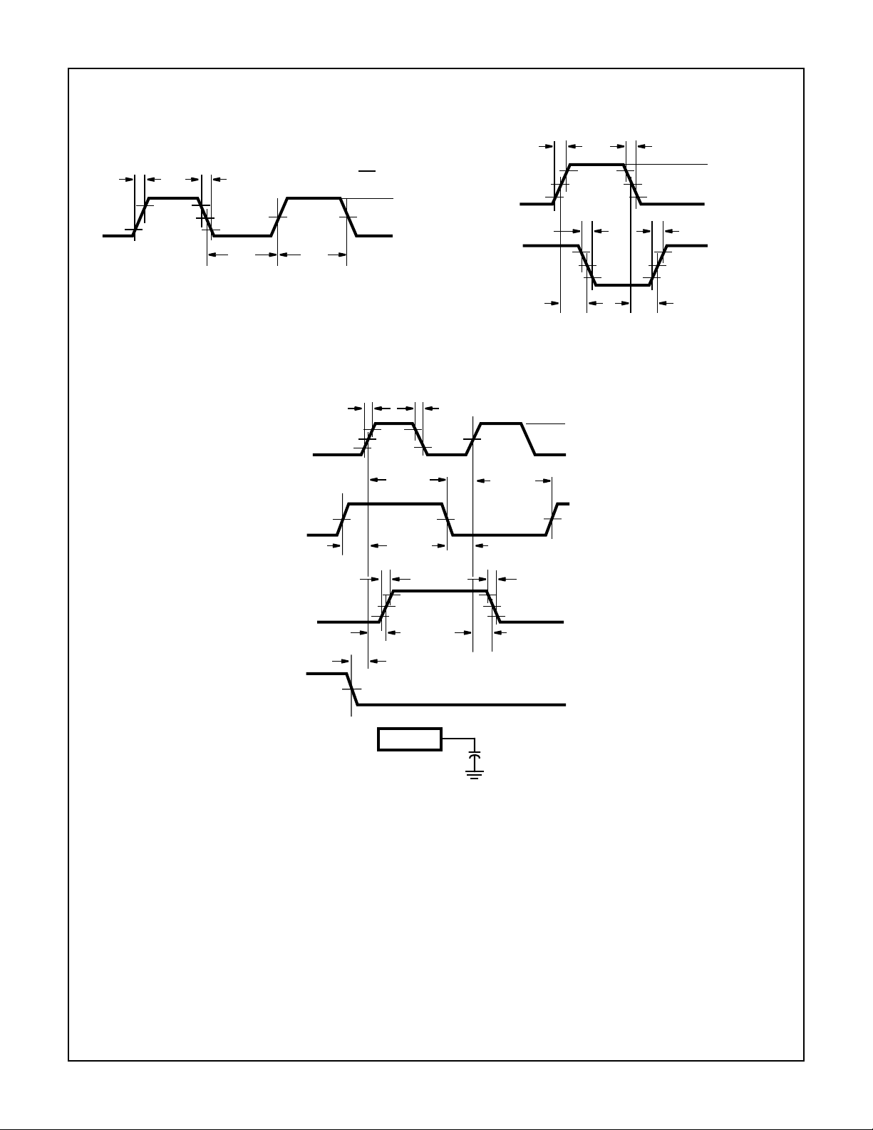
Test Circuits and Waveforms
trC
L
CLOCK
10%
90%
50%
10%
tfC
t
L
WL
tWL+ tWH=
50%
t
WH
NOTE: Outputs should be switching from 10% VCC to 90% VCC in
accordance with devicetruth table. For f
, input duty cycle = 50%.
MAX
FIGURE 2. HC CLOCK PULSE RISE AND FALLTIMES AND
PULSE WIDTH
fC
50%
I
L
V
CC
GND
tr = 6ns tf = 6ns
V
t
TLH
CC
GND
INPUT
INVERTING
OUTPUT
t
THL
t
PHL
90%
50%
10%
t
90%
50%
10%
PLH
FIGURE 3. HC TRANSITION TIMES AND PROPAGATION
DELAY TIMES, COMBINATION LOGIC
90%
t
PLH
IC
t
TLH
tfC
L
50%
t
H(L)
t
SU(L)
t
THL
90%
50%
10%
t
PHL
C
L
50pF
CLOCK
INPUT
DAT A
INPUT
t
SU(H)
OUTPUT
t
REM
V
CC
SET, RESET
OR PRESET
trC
L
90%
10%
t
H(H)
50%
FIGURE 4. HC SETUP TIMES, HOLD TIMES, REMOVAL
TIME, AND PROPAGATION DELAY TIMES FOR EDGE
TRIGGERED SEQUENTIAL LOGIC CIRCUITS
V
CC
GND
V
CC
50%
GND
GND
6

IMPORTANT NOTICE
T exas Instruments and its subsidiaries (TI) reserve the right to make changes to their products or to discontinue
any product or service without notice, and advise customers to obtain the latest version of relevant information
to verify, before placing orders, that information being relied on is current and complete. All products are sold
subject to the terms and conditions of sale supplied at the time of order acknowledgement, including those
pertaining to warranty, patent infringement, and limitation of liability.
TI warrants performance of its semiconductor products to the specifications applicable at the time of sale in
accordance with TI’s standard warranty. Testing and other quality control techniques are utilized to the extent
TI deems necessary to support this warranty . Specific testing of all parameters of each device is not necessarily
performed, except those mandated by government requirements.
CERTAIN APPLICATIONS USING SEMICONDUCTOR PRODUCTS MAY INVOLVE POTENTIAL RISKS OF
DEATH, PERSONAL INJURY, OR SEVERE PROPERTY OR ENVIRONMENTAL DAMAGE (“CRITICAL
APPLICATIONS”). TI SEMICONDUCTOR PRODUCTS ARE NOT DESIGNED, AUTHORIZED, OR
WARRANTED TO BE SUITABLE FOR USE IN LIFE-SUPPORT DEVICES OR SYSTEMS OR OTHER
CRITICAL APPLICA TIONS. INCLUSION OF TI PRODUCTS IN SUCH APPLICATIONS IS UNDERST OOD TO
BE FULLY AT THE CUSTOMER’S RISK.
In order to minimize risks associated with the customer’s applications, adequate design and operating
safeguards must be provided by the customer to minimize inherent or procedural hazards.
TI assumes no liability for applications assistance or customer product design. TI does not warrant or represent
that any license, either express or implied, is granted under any patent right, copyright, mask work right, or other
intellectual property right of TI covering or relating to any combination, machine, or process in which such
semiconductor products or services might be or are used. TI’s publication of information regarding any third
party’s products or services does not constitute TI’s approval, warranty or endorsement thereof.
Copyright 1998, Texas Instruments Incorporated
 Loading...