

Datasheet CD74HCT390E, CD74HCT390M96, CD74HCT390M, CD74HC390E, CD74HC390M96 Datasheet (Texas Instruments)
...
CD74HC390,
/
j
[ /Title
(CD74
HC390
,
CD74
HCT39
0)
Subect
(High
Speed
CMOS
Data sheet acquired from Harris Semiconductor
SCHS185
September 1997
Features
• Two BCD Decade or Bi-Quinary Counters
• One Package Can Be Configured to Divide-by-2, 4,
5,10, 20, 25, 50 or 100
• Two Master Reset Inputs to Clear Each Decade
Counter Individually
• Fanout (Over Temperature Range)
- Standard Outputs. . . . . . . . . . . . . . . 10 LSTTL Loads
- Bus Driver Outputs . . . . . . . . . . . . . 15 LSTTL Loads
• Wide Operating Temperature Range . . . -55
• Balanced Propagation Delay and Transition Times
• Significant Power Reduction Compared to LSTTL
Logic ICs
• HC Types
- 2V to 6V Operation
- High Noise Immunity: N
= 30%, NIH = 30% of V
IL
at VCC = 5V
• HCT Types
- 4.5V to 5.5V Operation
- Direct LSTTL Input Logic Compatibility,
V
= 0.8V (Max), VIH = 2V (Min)
IL
- CMOS Input Compatibility, I
≤ 1µA at VOL, V
l
o
C to 125oC
CC
OH
CD74HCT390
High Speed CMOS Logic
Dual Decade Ripple Counter
Description
The Harris CD74HC390 and CD574HCT390 dual 4-bit
decade ripple counters are high-speed silicon-gate CMOS
devices and are pin compatible with low-power Schottky TTL
(LSTTL). These devices are divided into four separately
clocked sections. The counters have two divide-by-2 sections and two divide-by-5 sections. These sections are normally used in a BCD decade or bi-quinary configuration,
since they share a common master reset (nMR). If the two
master reset inputs (1MR and 2MR) are used to simultaneously clear all 8 bits of the counter, a number of counting
configurations are possible within one package. The separate clock inputs (n
ple counter or frequency division applications of divide-by-2,
4. 5, 10, 20, 25, 50 or 100. Each section is triggered by the
High-to-Low transition of the input pulses (n
For BCD decade operation, the nQ0 output is connected to
the n
CP1 input of the divide-by-5 section. For bi-quinary
decade operation, the nO3 output is connected to the n
input and nQ
The master reset inputs (1MR and 2MR) are active-High
asynchronous inputs to each decade counter which operates on the portion of the counter identified by the “1” and “2”
prefixes in the pin configuration. A High level on the nMR
input overrides the clock and sets the four outputs Low.
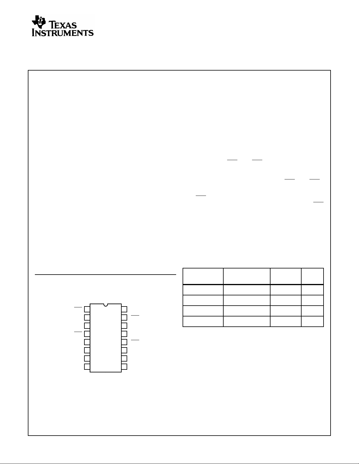
Ordering Information
CP0 and nCP1) of each section allow rip-
CP0 and nCP1).
becomes the decade output.
0
CP0
Pinout
CD74HC390, CD74HCT390
TOP VIEW
16
1
1CP0
1MR
2
1Q
3
0
4
1CP1
1Q
5
1
6
1Q
2
1Q
7
3
8
GND
CAUTION: These devices are sensitive to electrostatic discharge. Users should follow proper IC Handling Procedures.
Copyright
© Harris Corporation 1997
V
CC
15
2CP0
14
2MR
13
2Q0
12
2CP1
11
2Q
1
10
2Q
2
9
2Q
3
PART NUMBER TEMP. RANGE (oC) PACKAGE
CD74HC390E -55 to 125 16 Ld PDIP E16.3
CD74HCT390E -55 to 125 16 Ld PDIP E16.3
CD74HC390M -55 to 125 16 Ld SOIC M16.15
CD74HCT390M -55 to 125 16 Ld SOIC M16.15
NOTES:
1. When ordering, use the entire partnumber. Add the suffix 96 to
obtain the variant in the tape and reel.
2. Wafer for this part number is available which meets all electrical
specifications. Please contact your local sales office or Harris
customer service for ordering information.
1
PKG.
NO.
File Number 1838.2
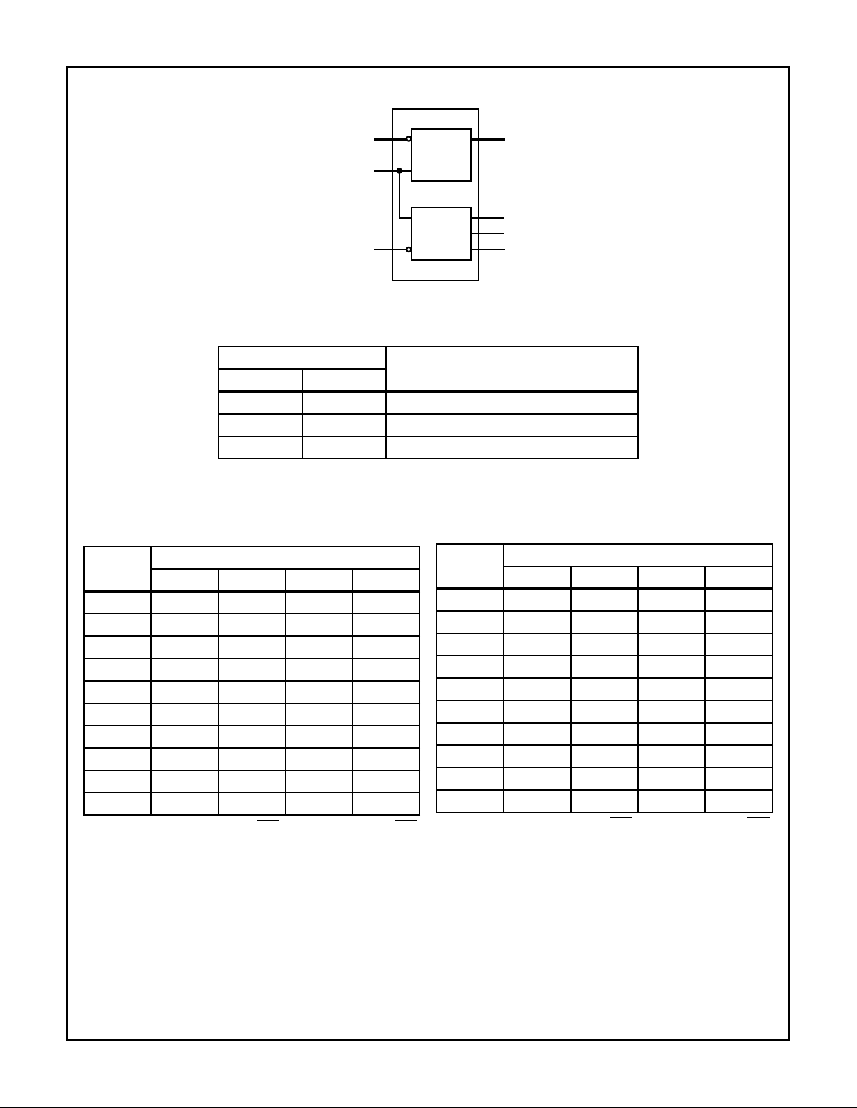
Functional Diagram
CD74HC390, CD74HCT390
1 (15)
nCP0
2 (14)
nMR
4 (12)
nCP1
GND = 8
V
= 16
CC
TRUTH TABLE
INPUTS
↑ L No Change
↓ L Count
X H All Qs Low
NOTE: H = High Voltage Level, L = Low Voltage Level, X = Don’t Care,
↑ = Transition from Low to High Level, ↓ = Transition from High to Low.
BCD COUNT SEQUENCE FOR 1/2 THE 390
OUTPUTS
COUNT
Q0 Q1 Q2 Q3
0LLLL
1HLLL
2LHLL
3HHLL
4LLHL
5HLHL
6LHHL
7HHHL
8LLLH
9HLLH
NOTE: Output nQ0 connected to nCP1 with counter input on nCP0.
3 (13)
nQ
nQ
nQ
nQ
0
1
2
3
÷ 2
COUNTER
÷ 5
COUNTER
5 (11)
6 (10)
7 (9)
ACTIONCP MR
B-QUINARY COUNT SEQUENCE FOR 1/2 THE 390
OUTPUTS
COUNT
Q0 Q1 Q2 Q3
0LLLL
1LHLL
2LLHL
3LHHL
4LLLH
5HLLL
6HHHL
7HLHL
8HHHL
9HLLH
NOTE: Output nQ3 connected to nCP0 with counter input on nCP1.
2
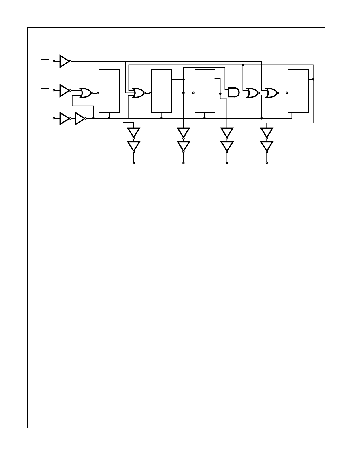
Logic Diagram
4(12)
CP1
n
CD74HC390, CD74HCT390
n
CP0
nMR
1(15)
2(14)
Q
Φ
R
3(13) 6(10) 7(9)
nQ
0
Q
Φ
R
5(11)
nQ
1
Q
Φ
R
VCC= 16
GND = 8
nQ
2
nQ
3
Q
Φ
R
3

CD74HC390, CD74HCT390
Absolute Maximum Ratings Thermal Information
DC Supply Voltage, VCC. . . . . . . . . . . . . . . . . . . . . . . . -0.5V to 7V
DC Input Diode Current, I
IK
For VI < -0.5V or VI > VCC + 0.5V. . . . . . . . . . . . . . . . . . . . . .±20mA
DC Output Diode Current, I
OK
For VO < -0.5V or VO > VCC + 0.5V . . . . . . . . . . . . . . . . . . . .±20mA
DC Output Source or Sink Current per Output Pin, I
O
For VO > -0.5V or VO < VCC + 0.5V . . . . . . . . . . . . . . . . . . . .±25mA
DC VCC or Ground Current, I
CC orIGND
. . . . . . . . . . . . . . . . . .±50mA
Operating Conditions
Temperature Range (TA) . . . . . . . . . . . . . . . . . . . . . -55oC to 125oC
Supply Voltage Range, V
HC Types . . . . . . . . . . . . . . . . . . . . . . . . . . . . . . . . . . . . .2V to 6V
HCT Types . . . . . . . . . . . . . . . . . . . . . . . . . . . . . . . . .4.5V to 5.5V
DC Input or Output Voltage, VI, VO . . . . . . . . . . . . . . . . . 0V to V
Input Rise and Fall Time
2V . . . . . . . . . . . . . . . . . . . . . . . . . . . . . . . . . . . . . . 1000ns (Max)
4.5V. . . . . . . . . . . . . . . . . . . . . . . . . . . . . . . . . . . . . . 500ns (Max)
6V . . . . . . . . . . . . . . . . . . . . . . . . . . . . . . . . . . . . . . . 400ns (Max)
CAUTION: Stresses above those listed in “Absolute Maximum Ratings” may cause permanent damage to the device. This is a stress only rating and operation
of the device at these or any other conditions above those indicated in the operational sections of this specification is not implied.
NOTE:
3. θJA is measured with the component mounted on an evaluation PC board in free air.
CC
Thermal Resistance (Typical, Note 3) θJA (oC/W)
PDIP Package. . . . . . . . . . . . . . . . . . . . . . . . . . . . . 90
SOIC Package. . . . . . . . . . . . . . . . . . . . . . . . . . . . . 190
Maximum Junction Temperature. . . . . . . . . . . . . . . . . . . . . . .150oC
Maximum Storage Temperature Range . . . . . . . . . .-65oC to 150oC
Maximum Lead Temperature (Soldering 10s). . . . . . . . . . . . .300oC
(SOIC - Lead Tips Only)
CC
DC Electrical Specifications
PARAMETER SYMBOL
HC TYPES
High Level Input
Voltage
Low Level Input
Voltage
High Level Output
Voltage
CMOS Loads
High Level Output
Voltage
TTL Loads
Low Level Output
Voltage
CMOS Loads
Low Level Output
Voltage
TTL Loads
Input Leakage
Current
Quiescent Device
Current
V
IH
V
IL
V
OH
V
OL
I
I
I
CC
TEST
CONDITIONS
(V) IO(mA) MIN TYP MAX MIN MAX MIN MAX
I
V
CC
(V)
o
C -40oC TO 85oC -55oCTO125oC
25
UNITSV
- - 2 1.5 - - 1.5 - 1.5 - V
4.5 3.15 - - 3.15 - 3.15 - V
6 4.2 - - 4.2 - 4.2 - V
- - 2 - - 0.5 - 0.5 - 0.5 V
4.5 - - 1.35 - 1.35 - 1.35 V
6 - - 1.8 - 1.8 - 1.8 V
VIHor VIL-0.02 2 1.9 - - 1.9 - 1.9 - V
-0.02 4.5 4.4 - - 4.4 - 4.4 - V
-0.02 6 5.9 - - 5.9 - 5.9 - V
- - ---- - - -V
-4 4.5 3.98 - - 3.84 - 3.7 - V
-5.2 6 5.48 - - 5.34 - 5.2 - V
VIHor VIL0.02 2 - - 0.1 - 0.1 - 0.1 V
0.02 4.5 - - 0.1 - 0.1 - 0.1 V
0.02 6 - - 0.1 - 0.1 - 0.1 V
- - ---- - - -V
4 4.5 - - 0.26 - 0.33 - 0.4 V
5.2 6 - - 0.26 - 0.33 - 0.4 V
VCC or
-6--±0.1 - ±1-±1µA
GND
VCC or
0 6 - - 8 - 80 - 160 µA
GND
4

CD74HC390, CD74HCT390
DC Electrical Specifications (Continued)
TEST
CONDITIONS
PARAMETER SYMBOL
HCT TYPES
High Level Input
Voltage
Low Level Input
Voltage
High Level Output
Voltage
V
IH
V
IL
V
OH
CMOS Loads
High Level Output
Voltage
TTL Loads
Low Level Output
Voltage
V
OL
CMOS Loads
Low Level Output
Voltage
TTL Loads
Input Leakage
Current
Quiescent Device
Current
Additional Quiescent
Device Current Per
I
I
I
CC
∆I
CC
Input Pin: 1 Unit Load
NOTE: For dual-supply systems theoretical worst case (V
(V) IO(mA) MIN TYP MAX MIN MAX MIN MAX
I
- - 4.5 to
- - 4.5 to
VIHor VIL-0.02 4.5 4.4 - - 4.4 - 4.4 - V
-4 4.5 3.98 - - 3.84 - 3.7 - V
VIHor VIL0.02 4.5 - - 0.1 - 0.1 - 0.1 V
4 4.5 - - 0.26 - 0.33 - 0.4 V
VCCand
0 5.5 - - ±0.1 - ±1-±1µA
GND
VCC or
0 5.5 - - 8 - 80 - 160 µA
GND
V
CC
- 4.5 to
-2.1
o
C -40oC TO 85oC -55oCTO125oC
V
CC
25
(V)
2--2- 2 - V
5.5
- - 0.8 - 0.8 - 0.8 V
5.5
- 100 360 - 450 - 490 µA
5.5
= 2.4V, VCC = 5.5V) specification is 1.8mA.
I
UNITSV
HCT Input Loading Table
INPUT UNIT LOADS
nCP0 0.45
nCP1, MR 0.6
NOTE: Unit Load is ∆ICClimit specified in DC Electrical Table, e.g.,
360µA max at 25oC.
Prerequisite for Switching Specifications
CHARACTERISTIC SYMBOL VCC (V)
HC TYPES
Maximum Clock
Frequency
Clock Pulse Width,
CP0, nCP1
n
Reset Removal Time t
f
MAX
t
REM
W
2 6--5-4-MHz
4.5 30 - - 24 - 20 - MHz
6 35- -28-24-MHz
2 80 - - 100 - 120 - ns
4.5 16 - - 20 - 24 - ns
6 14- -17-20-ns
2 70- -90-105-ns
4.5 14 - - 18 - 21 - ns
6 12- -15-18-ns
o
25
C -40oC TO 85oC -55oC TO 125oC
UNITSMIN TYP MAX MIN MAX MIN MAX
5

CD74HC390, CD74HCT390
Prerequisite for Switching Specifications (Continued)
CHARACTERISTIC SYMBOL V
Reset Pulse Width t
W
HCT TYPES
Maximum Clock
f
MAX
Frequency
Clock Pulse Width,
CP0, nCP1
n
Reset Removal Time t
Reset Pulse Width t
t
W
REM
W
(V)
CC
2 50- -65-75-ns
4.5 10 - - 13 - 15 - ns
6 9 - -11-13-ns
4.5 27 - - 22 - 18 - MHz
4.5 19 - - 24 - 29 - ns
4.5 15 - - 19 - 22 - ns
4.5 13 - - 16 - 20 - ns
o
25
C -40oC TO 85oC -55oC TO 125oC
UNITSMIN TYP MAX MIN MAX MIN MAX
Switching Specifications Input t
PARAMETER SYMBOL
HC TYPES
Propagation Delay (Figure 1) t
n
CP0 to nQ
n
CP1 to nQ
CP1 to nQ
n
CP1 to nQ
n
CP0 to nQ3
n
0
1
2
3
(nQ0 connected to nCP1)
MR to Q
n
Output Transition Time
(Figure 1)
Input Capacitance C
Power Dissipation Capacitance
(Notes 4, 5)
PLH,
t
PHL
t
PLH,
t
PHL
t
PLH,
t
PHL
t
PLH,
t
PHL
t
PLH,
t
PHL
t
PLH,
t
PHL
t
TLH,tTHLCL
C
, tf = 6ns
r
o
C -40oC TO 85oC -55oCTO125oC
TEST
CONDITIONS
V
CC
(V)
25
CL= 50pF 2 - - 175 - 220 - 265 ns
4.5 - - 35 - 44 - 53 ns
=15pF 5 - 14 - - - - - ns
C
L
= 50pF 6 - - 30 - 37 - 45 ns
C
L
CL= 50pF 2 - - 185 - 230 - 280 ns
4.5 - - 37 - 46 - 56 ns
6 - - 31 - 39 - 48 ns
CL= 50pF 2 - - 245 - 305 - 370 ns
4.5 - - 49 - 61 - 74 ns
6 - - 42 - 52 - 63 ns
CL= 50pF 2 - - 180 - 225 - 270 ns
4.5 - - 36 - 45 - 54 ns
5 - 15 - - - - - ns
6 - - 31 - 38 - 46 ns
CL= 50pF 2 - - 365 - 455 - 550 ns
4.5 - - 73 - 91 - 110 ns
6 - - 62 - 77 - 94 ns
CL= 50pF 2 - - 190 - 240 - 285 ns
4.5 - - 38 - 48 - 57 ns
=15pF 5 - 16 - - - - - ns
C
L
= 50pF 6 - - 32 - 41 - 48 ns
C
L
= 50pF 2 - - 75 - 95 - 110 ns
4.5 - - 15 - 19 - 22 ns
6 - - 13 - 16 - 19 ns
CL= 50pF - - - 10 - 10 - 10 pF
IN
CL=15pF 5 - 28 - - - - - pF
PD
UNITSMIN TYP MAX MIN MAX MIN MAX
6

CD74HC390, CD74HCT390
Switching Specifications Input t
PARAMETER SYMBOL
HCT TYPES
Propagation Delay (Figure 1) t
CP0 to nQ
n
n
CP1 to nQ
CP1 to nQ
n
CP1 to nQ
n
CP0 to nQ2
n
0
1
2
3
(nQ0 connected to nCP1)
MR to Q
n
Output Transition t
Input Capacitance C
Power Dissipation Capacitance
(Notes 4, 5)
NOTES:
is used to determine the dynamic power consumption, per multiplexer.
4. C
PD
5. PD = V
2
fi(CPD + CL) where fi = Input Frequency, CL = Output Load Capacitance, VCC = Supply Voltage.
CC
PLH,
t
PHL
t
PLH,
t
PHL
t
PLH,
t
PHL
t
PLH,
t
PHL
t
PLH,
t
PHL
t
PLH,
t
PHL
TLH,tTHLCL
C
, tf = 6ns (Continued)
r
o
25
TEST
CONDITIONS
V
CC
(V)
C -40oC TO 85oC -55oCTO125oC
CL= 50pF 4.5 - - 40 - 50 - 60 ns
CL=15pF 5 - 17 - - - - - ns
CL= 50pF 4.5 - - 43 - 51 - 65 ns
CL= 50pF 4.5 - - 55 - 69 - 83 ns
CL= 50pF 4.5 - - 42 - 53 - 63 ns
=15pF 5 - 18 - - - - - ns
C
L
CL= 50pF 4.5 - - 84 - 105 - 126 ns
CL= 50pF 4.5 - - 42 - 53 - 63 ns
C
=15pF 5 - 18 - - - - - ns
L
= 50pF 4.5 - - 15 - 19 - 22 ns
CL=15pF - - - 10 - 10 - 10 pF
IN
CL=15pF 5 - 32 - - - - - pF
PD
UNITSMIN TYP MAX MIN MAX MIN MAX
Test Circuits and Waveforms
tr = 6ns tf = 6ns
V
t
CC
GND
TLH
t
PHL
90%
50%
10%
t
90%
50%
10%
PLH
INPUT
t
INVERTING
OUTPUT
THL
FIGURE 1. HC AND HCU TRANSITION TIMES AND PROPAGA-
TION DELAY TIMES, COMBINATION LOGIC
= 6ns
t
PLH
t
f
1.3V
10%
90%
t
3V
GND
TLH
tr = 6ns
INPUT
t
INVERTING
OUTPUT
THL
t
PHL
2.7V
1.3V
0.3V
FIGURE 2. HCT TRANSITION TIMES AND PROPAGATION
DELAY TIMES, COMBINATION LOGIC
7

IMPORTANT NOTICE
T exas Instruments and its subsidiaries (TI) reserve the right to make changes to their products or to discontinue
any product or service without notice, and advise customers to obtain the latest version of relevant information
to verify, before placing orders, that information being relied on is current and complete. All products are sold
subject to the terms and conditions of sale supplied at the time of order acknowledgement, including those
pertaining to warranty, patent infringement, and limitation of liability.
TI warrants performance of its semiconductor products to the specifications applicable at the time of sale in
accordance with TI’s standard warranty. Testing and other quality control techniques are utilized to the extent
TI deems necessary to support this warranty . Specific testing of all parameters of each device is not necessarily
performed, except those mandated by government requirements.
CERT AIN APPLICATIONS USING SEMICONDUCTOR PRODUCTS MAY INVOLVE POTENTIAL RISKS OF
DEATH, PERSONAL INJURY, OR SEVERE PROPERTY OR ENVIRONMENTAL DAMAGE (“CRITICAL
APPLICATIONS”). TI SEMICONDUCTOR PRODUCTS ARE NOT DESIGNED, AUTHORIZED, OR
WARRANTED TO BE SUITABLE FOR USE IN LIFE-SUPPORT DEVICES OR SYSTEMS OR OTHER
CRITICAL APPLICA TIONS. INCLUSION OF TI PRODUCTS IN SUCH APPLICATIONS IS UNDERST OOD TO
BE FULLY AT THE CUSTOMER’S RISK.
In order to minimize risks associated with the customer’s applications, adequate design and operating
safeguards must be provided by the customer to minimize inherent or procedural hazards.
TI assumes no liability for applications assistance or customer product design. TI does not warrant or represent
that any license, either express or implied, is granted under any patent right, copyright, mask work right, or other
intellectual property right of TI covering or relating to any combination, machine, or process in which such
semiconductor products or services might be or are used. TI’s publication of information regarding any third
party’s products or services does not constitute TI’s approval, warranty or endorsement thereof.
Copyright 1999, Texas Instruments Incorporated
 Loading...