

1
Data sheet acquired from Harris Semiconductor
SCHS177
CD74HC297,
CD74HCT297
High-Speed CMOS Logic
Digital Phase-Locked-Loop
Features
• Digital Design Avoids Analog Compensation Errors
• Easily Cascadable for Higher Order Loops
• Useful Frequency Range
- K-Clock . . . . . . . . . . . . . . . . . . . . . . . . . .DC to 55MHz (Typ)
- I/D-Clock . . . . . . . . . . . . . . . . . . . . DC to 35MHz (Typ)
• Dynamically Variable Bandwidth
• Very Narrow Bandwidth Attainable
• Power-On Reset
• Output Capability
- Standard. . . . . . . . . . . . . . . . . . . . XORPD
OUT
, ECPD
OUT
- Bus Driver. . . . . . . . . . . . . . . . . . . . . . . . . . . . . I/D
OUT
• Fanout (Over Temperature Range)
- Standard Outputs . . . . . . . . . . . . . . . . . . 10 LSTTL Loads
- Bus Driver Outputs . . . . . . . . . . . . . 15 LSTTL Loads
• Balanced Propagation Delay and Transition Times
• Significant Power Reduction Compared to LSTTL
Logic ICs
• CD74HC297 Types
- Operation Voltage. . . . . . . . . . . . . . . . . . . . . . . . . . . 2 to 6V
- High Noise ImmunityN
IL
= 30%, NIH= 30% of VCC at 5V
• CD74HCT297 Types
- Operation Voltage. . . . . . . . . . . . . . . . . . . . . . . . 4.5 to 5.5V
- Direct LSTTL Input Logic Compatibility
V
IL
= 0.8V (Max), VIH= 2V (Min)
- CMOS Input Compatibility I
I
≤ 1µA at VOL, V
OH
Description
The Harris CD74HC297 and CD74HCT297 are high-speed
silicon gate CMOS devices that are pin-compatible with low
power Schottky TTL (LSTTL).
These devices are designed to provide a simple, cost-effective solution to high-accuracy,digital, phase-locked-loop applications. The y contain all the necessary circuits, with the
exception of the divide-by-N counter, to build first-order
phase-locked-loops.
Both EXCLUSIVE-OR (XORPD) and edge-controlled phase
detectors (ECPD) are provided for maximum flexibility. The
input signals for the EXCLUSIVE-OR phase detector must
have a 50% duty factor to obtain the maxim um loc k-range .
Proper partitioning of the loop function, with many of the building blocks external to the package, makes it easy for the
designer to incorporate ripple cancellation (see Figure 2) or to
cascade to higher order phase-locked-loops.
The length of the up/down K-counter is digitally programmable
according to the K-counter function table. With A, B, C and D
all LOW,the K-counter is disabled. With A HIGH and B, C and
D LOW,the K-counter is only three stages long, which widens
the bandwidth or capture range and shortens the lock time of
the loop. When A, B, C and D are all programmed HIGH, the
K-counter becomes sev enteen stages long, which narrows
the bandwidth or capture range and lengthens the lock time.
Real-time control of loop bandwidth by manipulating the A to
D inputs can maximize the overall performance of the digital
phase-locked-loop.
The CD74HC297 and CD74HCT297 can perform the classic
first order phase-locked-loop function without using analog
components. The accuracy of the digital phase-locked-loop
(DPLL) is not affected by V
CC
and temperature variations but
depends solely on accuracies of the K-clock and loop propagation delays.
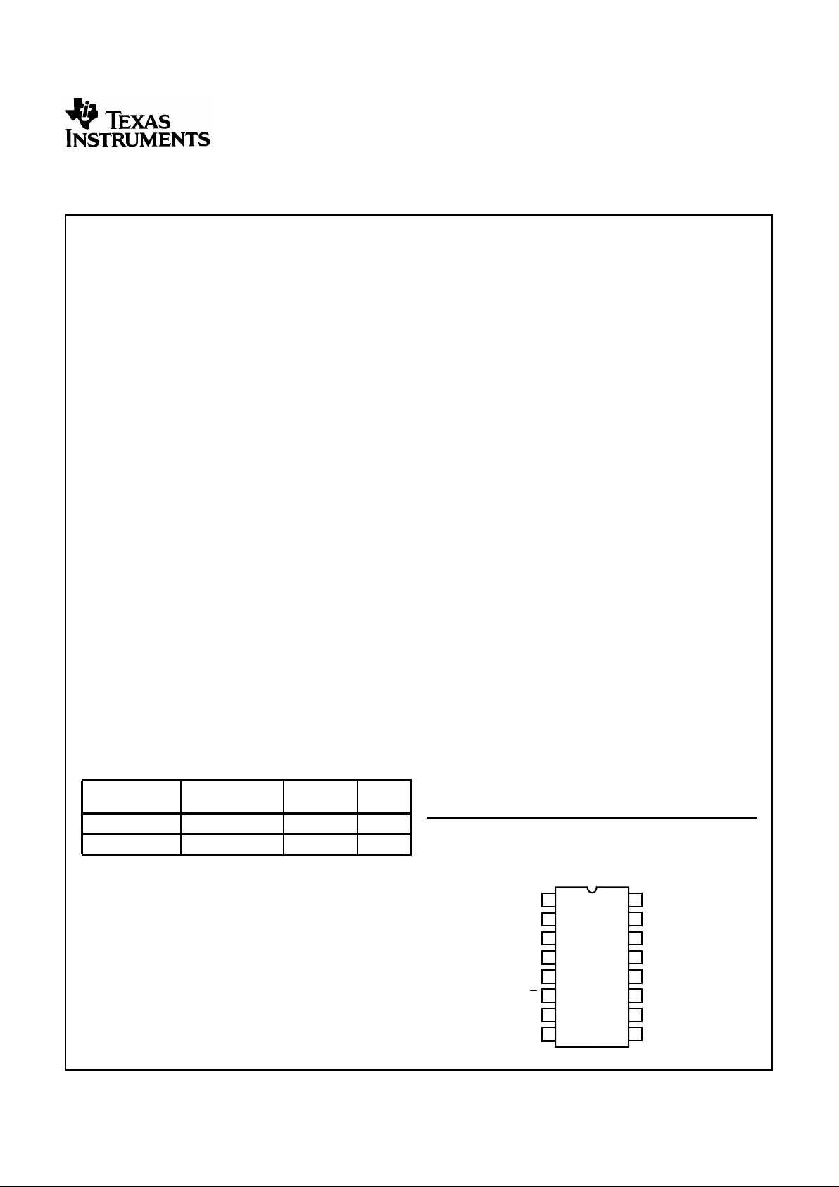
Pinout
CD74HC297, CD74HCT297 (PDIP)
TOP VIEW
Ordering Information
PART NUMBER TEMP.RANGE(oC) PACKAGE
PKG.
NO.
CD74HC297E -55 to 125 16 Ld PDIP E16.3
CD74HCT297E -55 to 125 16 Ld PDIP E16.3
NOTES:
1. When ordering, use the entire part number. Add the suffix 96 to
obtain the variant in the tape and reel.
2. Wafer or diefor thispartnumber isavailablewhich meetsallelectrical specifications. Please contact your local sales office or
Harris customer service for ordering information.
14
15
16
9
13
12
11
10
1
2
3
4
5
7
6
8
B
A
EN
CTR
K
CP
I/D
CP
D/U
GND
I/D
OUT
V
CC
D
φA
2
ECPD
OUT
XORPD
OUT
φB
φA
1
C
November 1997
CAUTION: These devices are sensitive to electrostatic discharge. Users should follow proper IC Handling Procedures.
Copyright
© Harris Corporation 1997
File Number 1852.1
[ /Title
(CD74
HC297
,
CD74
HCT29
7)
/
Sub-
j
ect
(HighSpeed
CMOS
Logic
Digital
PhaseLocked
2
The phase detector generates an error signal waveform that,
at zero phase error, is a 50% duty factor square wave. At the
limits of linear operation, the phase detector output will be
either HIGH or LOW all of the time depending on the direction
of the phase error (φIN - φOUT). Within these limits the phase
detector output varies linearly with the input phase error
according to the gain K
d
, which is expressed in terms of
phase detector output per cycle or phase error. The phase
detector output can be defined to vary between ±1 according
to the relation:
The output of the phase detector will be K
dφe
, where the
phase error φ
e
= φIN - φOUT.
EXCLUSIVE-OR phase detectors (XORPD) and edge-controlled phase detectors (ECPD) are commonly used digital
types. The ECPD is more complex than the XORPD logic
function but can be described generally as a circuit that
changes states on one of the transitions of its inputs. The gain
(K
d
) for an XORPD is 4 because its output remains HIGH
(XORPD
OUT
= 1) for a phase error of one quarter cycle.
Similarly , K
d
for the ECPD is 2 since its output remains HIGH
for a phase error of one half cycle. The type of phase detector
will determine the zero-phase-error point, i.e., the phase separation of the phase detector inputs for a φe defined to be
zero. For the basic DPLL system of Figure 3, φe = 0 when the
phase detector output is a square wave.
The XORPD inputs are one quarter cycle out-of-phase for
zero phase error. For the ECPD, φe = 0 when the inputs are
one half cycle out of phase.
The phase detector output controls the up/down input to the
K-counter. The counter is clocked by input frequency Mf
c
which is a multiple M of the loop center frequency fc. When
the K-counter recycles up, it generates a carry pulse. Recycling while counting down generates a borrow pulse. If the
carry and the borrow outputs are conceptually combined into
one output that is positive for a carry and negative for a borrow, and if the K-counter is considered as a frequency divider
with the ratio Mf
c
/K, the output of the K-counter will equal the
input frequency multiplied by the division ratio. Thus the output from the K-counter is (K
dφeMfc
)/K.
The carry and borrow pulses go to the increment/decrement
(I/D) circuit which, in the absence of any carry or borrow
pulses has an output that is one half of the input clock (I/D
CP
).
The input clock is just a multiple, 2N, of the loop center frequency. In response to a carry of borrow pulse, the I/D circuit
will either add or delete a pulse at I/D
OUT
. Thus the output of
the I/D circuit will be Nf
c
+ (KdφeMfc)/2K.
The output of the N-counter (or the output of the phaselocked-loop) is thus: fo = fc + (KdφeMfc)/2KN.
If this result is compared to the equation for a first-order analog phase-locked-loop, the digital equivalent of the gain of the
VCO is just Mf
c
/2KN or fc/K for M = 2N.
Thus, the simple first-order phase-locked-loop with an adjustable K-counter is the equivalent of an analog phase-lockedloop with a programmable VCO gain.
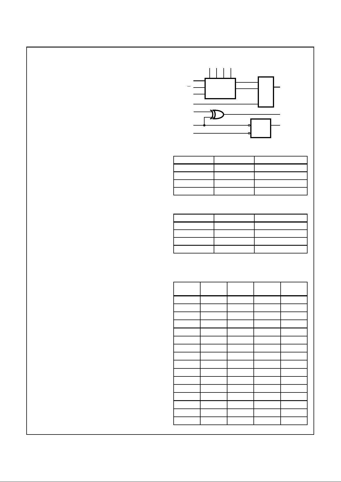
Functional Diagram
phase detector output =
%HIGH - %LOW
100
--------------------------------------------
FUNCTION TABLE
EXCLUSIVE-OR PHASE DETECTOR
φA
1
φB XORPD OUT
LL L
LH H
HL H
HH L
FUNCTION TABLE
EDGE-CONTROLLED PHASE DETECTOR
φA
2
φB ECPD OUT
H or L
↓
H
↓
H or L L
H or L ↑ No Change
↑ H or L No Change
H=Steady-State High Level,L= Steady-StateLowLevel, ↑=LOW
to HIGH φ Transition,↓ = HIGH to LOW φ Transition
K-COUNTER FUNCTION TABLE
(DIGITAL CONTROL)
DCBA
MODULO
(K)
LLLLInhibited
LLLH2
3
LLHL2
4
LLHH2
5
LHLL2
6
LHLH2
7
LHHL2
8
LHHH2
9
HLLL2
10
HLLH2
11
HLHL2
12
HLHH2
13
HHL L2
14
HHLH2
15
HHHL2
16
HHHH2
17
MODULO-K
COUNTER
K
CP
D/U
EN
CTR
4
6
3
5
9
10
13
14 15 1 2
CARRY
BORROW
I/D
CKT
DCBA
I/D
CP
φA
1
φB
φA
2
J
F/F
Q
K
7
11
12
I/D
OUT
XORPD
OUT
ECPD
OUT
CD74HC297, CD74HCT297CD74HC297, CD74HCT297
3
Absolute Maximum Ratings Thermal Information
DC Supply Voltage, VCC. . . . . . . . . . . . . . . . . . . . . . . . -0.5V to 7V
DC Input Diode Current, I
IK
For VI < -0.5V or VI > VCC + 0.5V. . . . . . . . . . . . . . . . . . . . . .±20mA
DC Output Diode Current, I
OK
For VO < -0.5V or VO > VCC + 0.5V . . . . . . . . . . . . . . . . . . . .±20mA
DC Drain Current, per Output, I
O
For -0.5V < VO < VCC + 0.5V. . . . . . . . . . . . . . . . . . . . . . . . . .±25mA
DC Output Source or Sink Current per Output Pin, I
O
For VO > -0.5V or VO < VCC + 0.5V . . . . . . . . . . . . . . . . . . . .±25mA
DC VCC or Ground Current, ICC . . . . . . . . . . . . . . . . . . . . . . . . .±50mA
Operating Conditions
Temperature Range, TA . . . . . . . . . . . . . . . . . . . . . . -55oC to 125oC
Supply Voltage Range, V
CC
HC Types . . . . . . . . . . . . . . . . . . . . . . . . . . . . . . . . . . . . .2V to 6V
HCT Types . . . . . . . . . . . . . . . . . . . . . . . . . . . . . . . . .4.5V to 5.5V
DC Input or Output Voltage, VI, VO . . . . . . . . . . . . . . . . . 0V to V
CC
Input Rise and Fall Time
2V . . . . . . . . . . . . . . . . . . . . . . . . . . . . . . . . . . . . . . 1000ns (Max)
4.5V. . . . . . . . . . . . . . . . . . . . . . . . . . . . . . . . . . . . . . 500ns (Max)
6V . . . . . . . . . . . . . . . . . . . . . . . . . . . . . . . . . . . . . . . 400ns (Max)
Thermal Resistance (Typical, Note 2) θJA (oC/W)
PDIP Package. . . . . . . . . . . . . . . . . . . . . . . . . . . . . 90
Maximum Junction Temperature. . . . . . . . . . . . . . . . . . . . . . . 150oC
Maximum Storage Temperature Range . . . . . . . . . .-65oC to 150oC
Maximum Lead Temperature (Soldering 10s). . . . . . . . . . . . . 300oC
CAUTION: Stresses above those listed in “Absolute Maximum Ratings” may cause permanent damage to the device. This is a stress only rating and operation
of the device at these or any other conditions above those indicated in the operational sections of this specification is not implied.
NOTE:
3. θJA is measured with the component mounted on an evaluation PC board in free air.
DC Electrical Specifications
PARAMETER SYMBOL
TEST
CONDITIONS
VCC (V)
25oC -40oC TO 85oC -55oC TO 125oC
UNITSVI(V) IO(mA) MIN TYP MAX MIN MAX MIN MAX
HC TYPES
High Level Input
Voltage
V
IH
- - 2 1.5 - - 1.5 - 1.5 - V
4.5 3.15 - - 3.15 - 3.15 - V
6 4.2 - - 4.2 - 4.2 - V
Low Level Input
Voltage
V
IL
- - 2 - - 0.5 - 0.5 - 0.5 V
4.5 - - 1.35 - 1.35 - 1.35 V
6 - - 1.8 - 1.8 - 1.8 V
High Level Output
Voltage
CMOS Loads
V
OH
VIH or
V
IL
-0.02 2 1.9 - - 1.9 - 1.9 - V
-0.02 4.5 4.4 - - 4.4 - 4.4 - V
-0.02 6 5.9 - - 5.9 - 5.9 - V
High Level Output
Voltage
TTL Loads
-6
(Note 4)
4.5 3.98 - - 3.84 - 3.7 - V
-7.8
(Note 4)
6 5.48 - - 5.34 - 5.2 - V
Low Level Output
Voltage
CMOS Loads
V
OL
VIH or
V
IL
0.02 2 - - 0.1 - 0.1 - 0.1 V
0.02 4.5 - - 0.1 - 0.1 - 0.1 V
0.02 6 - - 0.1 - 0.1 - 0.1 V
Low Level Output
Voltage
TTL Loads
4
(Note 4)
4.5 - - 0.26 - 0.33 - 0.4 V
5.2
(Note 4)
6 - - 0.26 - 0.33 - 0.4 V
CD74HC297, CD74HCT297CD74HC297, CD74HCT297
4
Input Leakage
Current
I
I
VCC or
GND
-6--±0.1 - ±1-±1 µA
Quiescent Device
Current
I
CC
VCC or
GND
0 6 - - 8 - 80 - 160 µA
HCT TYPES
High Level Input
Voltage
V
IH
- - 4.5 to
5.5
2-- 2 - 2 - V
Low Level Input
Voltage
V
IL
- - 4.5 to
5.5
- - 0.8 - 0.8 - 0.8 V
High Level Output
Voltage
CMOS Loads
V
OH
VIH or
V
IL
-0.02 4.5 4.4 - - 4.4 - 4.4 - V
High Level Output
Voltage
TTL Loads
-4 4.5 3.98 - - 3.84 - 3.7 - V
Low Level Output
Voltage
CMOS Loads
V
OL
VIH or
V
IL
0.02 4.5 - - 0.1 - 0.1 - 0.1 V
Low Level Output
Voltage
TTL Loads
4 4.5 - - 0.26 - 0.33 - 0.4 V
Input Leakage
Current
I
I
VCC to
GND
0 5.5 - - ±0.1 - ±1-±1 µA
Quiescent Device
Current
I
CC
VCC or
GND
0 5.5 - - 8 - 80 - 160 µA
Additional Quiescent
Device Current Per
Input Pin: 1 Unit Load
(Note 3)
∆I
CC
V
CC
-2.1
- 4.5 to
5.5
- 100 360 - 450 - 490 µA
NOTE:
4. For dual-supply systems theoretical worst case (VI = 2.4V, VCC = 5.5V) specification is 1.8mA.
5. XORPD, ECPD
DC Electrical Specifications (Continued)
PARAMETER SYMBOL
TEST
CONDITIONS
VCC (V)
25oC -40oC TO 85oC -55oC TO 125oC
UNITSVI(V) IO(mA) MIN TYP MAX MIN MAX MIN MAX
HCT Input Loading Table
INPUT UNIT LOADS
EN
CTR
, D/U 0.3
A, B, C, D, KCP, φA
2
0.6
I/DCP, φA1, φB 1.5
NOTE: Unit Load is ∆ICClimit specified in DC Electrical
Specifications table, e.g., 360µA max at 25oC.
CD74HC297, CD74HCT297CD74HC297, CD74HCT297

5
Prerequisite For Switching Function
PARAMETER SYMBOL VCC (V)
25oC -40oC TO 85oC -55oC TO 125oC
UNITSMIN MAX MIN MAX MIN MAX
HC TYPES
Maximum Clock Frequency
K
CP
f
MAX
26-5-4-MHz
4.5 30 - 24 - 20 - MHz
6 35 - 28 - 24 - MHz
Maximum Clock Frequency
I/D
CP
f
MAX
24-3-2-MHz
4.5 20 - 16 - 13 - MHz
6 24 - 19 - 15 - MHz
Clock Pulse Width
K
CP
t
w
2 80 - 100 - 120 - ns
4.5 16 - 20 - 24 - ns
614-17-20-ns
Clock Pulse Width
I/D
CP
t
W
2 125 - 155 - 190 - ns
4.5 25 - 31 - 38 - ns
621-26-32-ns
Set-up Time
D/U, EN
CTR
to K
CP
t
SU
2 100 - 125 - 150 - ns
4.5 20 - 25 - 30 - ns
617-21-26-ns
Hold Time
D/U, EN
CTR
to K
CP
t
H
20-0-0-ns
4.50-0-0-ns
60-0-0-ns
HCT TYPES
Maximum Clock Frequency
K
CP
f
MAX
4.5 30 - 24 - 20 - MHz
Maximum Clock Frequency
I/D
CP
f
MAX
4.5 20 - 16 - 13 - MHz
Clock Pulse Width
K
CP
t
w
4.5 16 - 20 - 24 - ns
Clock Pulse Width
I/D
CP
t
w
4.5 25 - 31 - 38 - ns
Set-up Time
D/U, EN
CTR
to K
CP
t
SU
4.5 20 - 25 - 30 - ns
Hold Time
D/U, EN
CTR
to K
CP
t
H
4.50-0-0-ns
Switching Specifications Input t
r
, tf = 6ns
PARAMETER SYMBOL
TEST
CONDITIONS VCC (V)
25oC -40oC TO 85oC -55oC TO 125oC
UNITSTYP MAX MAX MAX
HC TYPES
Propagation Delay,
I/DCP to I/D
OUT
t
PLH
, t
PHLCL
= 50pF 2 - 175 220 265 ns
4.5 - 35 44 53 ns
6 - 30 34 43 ns
CD74HC297, CD74HCT297CD74HC297, CD74HCT297

6
Propagation Delay,
φA1, φB to XORPD
OUT
t
PLH
, t
PHLCL
= 50pF 2 - 150 190 225 ns
4.5 - 30 38 45 ns
6 - 26 33 38 ns
Propagation Delay,
φB, φA2 to ECPD
OUT
t
PHL
, t
PHLCL
= 50pF 2 - 200 250 300 ns
4.5 - 40 50 60 ns
6 - 34 43 51 ns
Output Transition Time
XORPD
OUT
ECPD
OUT
t
TLH
CL= 50pF 2 - 75 95 110 ns
4.5 - 15 19 22 ns
6 - 13 16 19 ns
Output Transition Time
I/D
OUT
t
TLH
CL= 50pF 2 - 60 75 90 ns
4.5 - 12 15 18 ns
6 - 10 13 15 ns
Input Capacitance C
I
---1010 10pF
HCT TYPES
Propagation Delay,
I/DCP to I/D
OUT
t
PLH
, t
PHLCL
= 50pF 4.5 - 35 44 53 ns
Propagation Delay,
φA1, φB to XORPD
OUT
t
PLH
, t
PHLCL
= 50pF 4.5 - 30 38 45 ns
Propagation Delay,
φB, φA2 to ECPD
OUT
t
PHL
, t
PHLCL
= 50pF 4.5 - 40 50 60 ns
Output Transition Time
XORPD
OUT
t
TLH
CL= 50pF 4.5 - 15 19 22 ns
Output Transition Time
ECPD
OUT
t
TLH
CL= 50pF 4.5 - 12 15 18 ns
Input Capacitance C
I
---1010 10pF
Switching Specifications Input t
r
, tf = 6ns (Continued)
PARAMETER SYMBOL
TEST
CONDITIONS VCC (V)
25oC -40oC TO 85oC -55oC TO 125oC
UNITSTYP MAX MAX MAX
CD74HC297, CD74HCT297CD74HC297, CD74HCT297

7
Logic Diagram
D
CP
FF
Q
D
CP
FF
Q
R
D
T
FF
Q
R
D
T
FF
Q
R
D
T
FF1
Q
R
D
T
FF
Q
R
D
T
FF
Q
R
D
T
FF1
Q
M
D
M
D
R
D
T
FF13
Q
M
D
R
D
T
FF14
Q
M
D
R
D
T
FF
Q
R
D
T
FF
Q
R
D
T
FF14
Q
M
D
R
D
FF13
Q
M
D
D
CP
FF
Q
Q
D
CP
FF
Q
Q
D
CP
FF
Q
Q
D
CP
FF
Q
Q
D
CP
FF
Q
D
CP
FF
Q
D
CP
FF
Q
D
CP
FF
Q
CP
FF
Q
J
KQ
R
D
FF
Q
S
D
Q
R
D
FF
Q
S
D
Q
A
B
C
D
2
1
15
14
4
6
K
CP
D/U
1
2
4
8
0
CONTROL CIRCUIT
1413121110987654321
TO MODE CONTROLS 12-2
(11 STAGES NOT SHOWN)
MODULO-K COUNTER
EN
CTR
3
POWER ON RESET
1 = 1 1
I/D
CP
5
INCREMENT/DECREMENT CIRCUIT
BORROW
CARRY
I/D
OUT
7
XORPD
OUT
11
ECPD
OUT
12
EXCLUSIVE-OR PHASE DETECTOR
EDGE-CONTROLLED PHASE DETECTOR
φA
2
φB
φA
1
9
10
13
T
CD74HC297, CD74HCT297CD74HC297, CD74HCT297

8
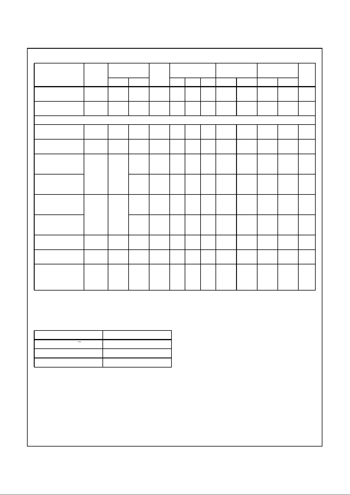
FIGURE 1. DPLL USING BOTH PHASE DETECTORS IN A RIPPLE-CANCELLATION SCHEME
FIGURE 2. DPLL USING EXCLUSIVE-OR PHASE DETECTION
FIGURE 3. TIMING DIAGRAM: I/D
OUT
IN-LOCK CONDITION
DIVIDE-BY-K
COUNTER
EN
CTR
K
CP
D/U
CARRY
BORROW
XORPD
OUT
JJ
ECPD
K
FF
ECPD
OUT
φA
1
φB
φA
2
DIVIDE-BY-N
COUNTER
I/D
OUT
I/D
CP
I/D CIRCUIT
2Nf
C
Mf
C
f
OUT
φ
OUT
f
IN
φ
IN
DIVIDE-BY-K
COUNTER
K
CP
D/U
CARRY
BORROW
XORPD
OUT
φA
1
φB
DIVIDE-BY-N
COUNTER
I/D
OUT
I/D
CP
I/D CIRCUIT
2Nf
C
Mf
C
f
OUT
φ
IN
f
OUT
φ
OUT
CARRY PULSE
(INTERNAL SIGNAL)
BORROW PULSE
(INTERNAL SIGNAL)
I/D
CP
INPUT
I/D
OUT
OUTPUT
CD74HC297, CD74HCT297CD74HC297, CD74HCT297

9
FIGURE 4. TIMING DIAGRAM: EDGE CONTROLLED PHASE COMPARATOR WAVEFORMS
FIGURE 5. TIMING DIAGRAM: EXCLUSIVE OR PHASE DETECTOR WAVEFORMS
FIGURE 6. WAVEFORMS SHOWINGTHE CLOCK (I/DCP) TO OUTPUT (I/D
OUT
) PROPAGATION DELAYS, CLOCK PULSE WIDTH,
OUTPUT TRANSITION TIMES AND MAXIMUM CLOCK PULSE FREQUENCY
FIGURE 7. WAVEFORMS SHOWING THE PHASE INPUT (øB, øA1) TO OUTPUT (XORPD
OUT
) PROPAGATION DELAYS AND
OUTPUT TRANSITION TIMES
øB INPUT
øA
2
INPUT
ECPD
OUT
OUTPUT
øB INPUT
XORPD
OUT
OUTPUT
øA
1
INPUT
I/f
MAX
t
W
I/D
CP
V
S
t
PLH
I/D
OUT
t
TLH
t
THL
V
S
t
PHL
V
S
øB INPUT
V
S
V
S
øA1 INPUT
XORPD
OUT
OUTPUT
t
PLH
t
PLH
t
THL
t
PLH
t
PHL
t
TLH
CD74HC297, CD74HCT297

10
FIGURE 8. WAVEFORMSSHOWING THE PHASE INPUT (øB, øA2) TOOUTPUT(ECPD
OUT
) PROPAGATION DELAYSANDOUTPUT
TRANSITION TIMES
NOTE: The shaded areas indicate when the input is permitted to change for predictable output performance.
FIGURE 9. WAVEFORMS SHOWINGTHE CLOCK (KCP) PULSE WIDTH AND MAXIMUM CLOCK PULSE FREQUENCY, AND THE
INPUT (D/U, EN
CTR
) TO CLOCK (KCP) SETUP AND HOLD TIMES
øB INPUT
V
S
V
S
V
S
t
PHL
t
PLH
t
TLH
t
THL
øA2 INPUT
OUTPUT
ECPD
OUT
D/U, EN
CTR
t
H
V
S
V
S
t
SU
t
SU
t
W
1/f
MAX
t
H
INPUT
KCP INPUT
CD74HC297, CD74HCT297

IMPORTANT NOTICE
T exas Instruments and its subsidiaries (TI) reserve the right to make changes to their products or to discontinue
any product or service without notice, and advise customers to obtain the latest version of relevant information
to verify, before placing orders, that information being relied on is current and complete. All products are sold
subject to the terms and conditions of sale supplied at the time of order acknowledgement, including those
pertaining to warranty, patent infringement, and limitation of liability.
TI warrants performance of its semiconductor products to the specifications applicable at the time of sale in
accordance with TI’s standard warranty. Testing and other quality control techniques are utilized to the extent
TI deems necessary to support this warranty. Specific testing of all parameters of each device is not necessarily
performed, except those mandated by government requirements.
CERT AIN APPLICATIONS USING SEMICONDUCTOR PRODUCTS MAY INVOLVE POTENTIAL RISKS OF
DEATH, PERSONAL INJURY, OR SEVERE PROPERTY OR ENVIRONMENTAL DAMAGE (“CRITICAL
APPLICATIONS”). TI SEMICONDUCTOR PRODUCTS ARE NOT DESIGNED, AUTHORIZED, OR
WARRANTED TO BE SUITABLE FOR USE IN LIFE-SUPPORT DEVICES OR SYSTEMS OR OTHER
CRITICAL APPLICATIONS. INCLUSION OF TI PRODUCTS IN SUCH APPLICA TIONS IS UNDERSTOOD T O
BE FULLY AT THE CUSTOMER’S RISK.
In order to minimize risks associated with the customer’s applications, adequate design and operating
safeguards must be provided by the customer to minimize inherent or procedural hazards.
TI assumes no liability for applications assistance or customer product design. TI does not warrant or represent
that any license, either express or implied, is granted under any patent right, copyright, mask work right, or other
intellectual property right of TI covering or relating to any combination, machine, or process in which such
semiconductor products or services might be or are used. TI’s publication of information regarding any third
party’s products or services does not constitute TI’s approval, warranty or endorsement thereof.
Copyright 1998, Texas Instruments Incorporated
 Loading...