

Texas Instruments CD74HCT259M96, CD74HCT259M, CD74HCT259E, CD74HC259M96, CD74HC259M Datasheet
...
Data sheet acquired from Harris Semiconductor
/
j
SCHS173
November 1997
CD74HC259,
CD74HCT259
High Speed CMOS Logic
8-Bit Addressable Latch
[ /Title
(CD74
HC259
,
CD74
HCT25
9)
Subect
(High
Speed
CMOS
Logic
8-Bit
Addres
sable
Latch)
Features
• Buffered Inputs and Outputs
• Four Operating Modes
• Typical Propagation Delay of 15ns at V
C
= 15pF, TA = 25oC
L
• Fanout (Over Temperature Range)
- Standard Outputs. . . . . . . . . . . . . . . 10 LSTTL Loads
- Bus Driver Outputs . . . . . . . . . . . . . 15 LSTTL Loads
• Wide Operating Temperature Range . . . -55
• Balanced Propagation Delay and Transition Times
• Significant Power Reduction Compared to LSTTL
Logic ICs
• HC Types
- 2V to 6V Operation
- High Noise Immunity: N
at VCC = 5V
• HCT Types
- 4.5V to 5.5V Operation
- Direct LSTTL Input Logic Compatibility,
V
= 0.8V (Max), VIH = 2V (Min)
IL
- CMOS Input Compatibility, I
= 30%, NIH = 30% of V
IL
≤ 1µA at VOL, V
l
CC
= 5V,
o
C to 125oC
OH
Description
The Harris CD74HC259 and CD74HCT259 Addressable
Latch features the low-power consumption associated with
CMOS circuitry and has speeds comparable to low-power
Schottky.
This latches three active modes and one reset mode. When
both the Latch Enable (
low (8-line Demultiplexer mode) the output of the addressed
latch follows the Data input and all other outputs are forced
low . When both
outputs are isolated from the Data input, i.e., all latches hold
the last data presented before the
high. A condition of
mode) allows the addressed latch’s output to follow the data
input; all other latches are unaffected. The Reset mode (all
outputs low) results when
LE) and Master Reset (MR) inputs are
MR and LE are high (Memory Mode), all
LE transition from low to
LE low and MR high (Addressable Latch
LE is high and MR is low.
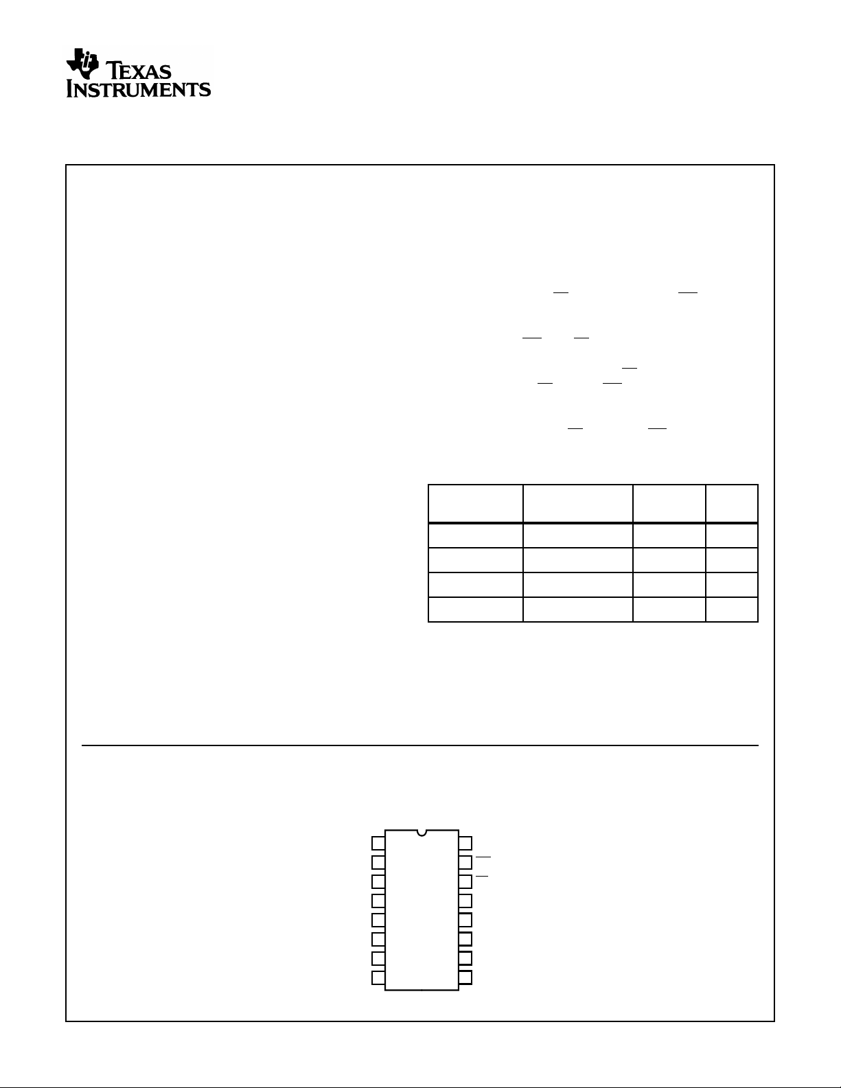
Ordering Information
CC
PART NUMBER TEMP. RANGE (oC) PACKAGE
CD74HC259E -55 to 125 16 Ld PDIP E16.3
CD74HCT259E -55 to 125 16 Ld PDIP E16.3
CD74HC259M -55 to 125 16 Ld SOIC M16.15
CD74HCT259M -55 to 125 16 Ld SOIC M16.15
PKG.
NO.
Pinout
NOTES:
1. When ordering, use the entire part number. Add the suffix 96 to
obtain the variant in the tape and reel.
2. Wafer or dieforthis part numberis available whichmeetsall electrical specifications. Please contact your local sales office or
Harris customer service for ordering information.
CD74HC259, CD74HCT259
(PDIP, SOIC)
TOP VIEW
A0
A1
A2
Q0
Q1
Q2
Q3
GND
1
2
3
4
5
6
7
8
16
15
14
13
12
11
10
9
V
MR
LE
D
Q7
Q6
Q5
Q4
CC
CAUTION: These devices are sensitive to electrostatic discharge. Users should follow proper IC Handling Procedures.
Copyright
© Harris Corporation 1997
1
File Number 1727.1
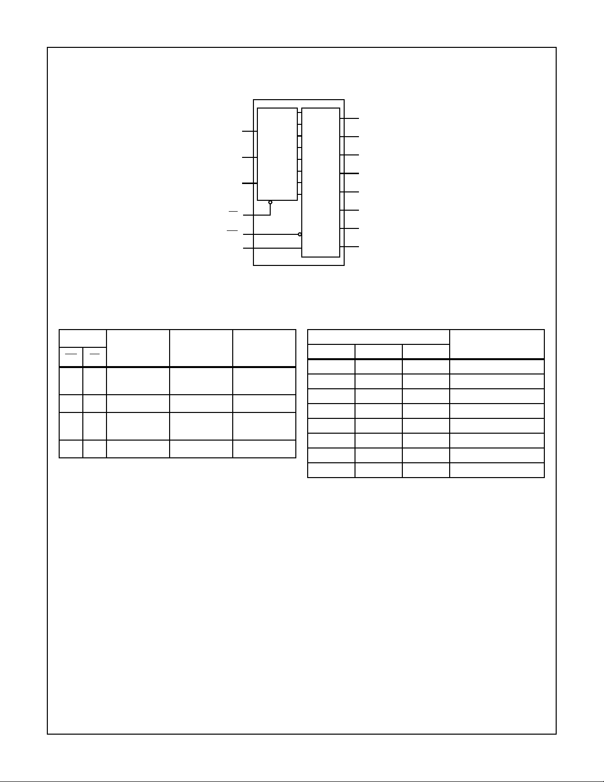
Functional Diagram
CD74HC259, CD74HCT259
4
Q0
5
Q1
6
Q2
7
Q3
9
Q4
10
Q5
11
Q6
12
Q7
GND = 8
= 16
V
CC
A
A
A
LE
MR
1
0
2
1
2
D
1-OF-8
DECODER
3
14
15
13
8
LATCHES
TRUTH TABLE
INPUTS OUTPUT OF
ADDRESS
LATCH
EACH OTHER
OUTPUT FUNCTIONMR LE
HL D QioAddressable
Latch
HH Q
io
Q
io
Memory
L L D L 8-Line
Demultiplexer
L H L L Reset
NOTE:
H = High Voltage Level
L = Low Voltage Level
D = The level at the data input
Qio= The levelof Qi(i = 0, 1...7, as appropriate) before theindicated
steady-state input conditions were established.
LATCH SELECTION TABLE
SELECT INPUTS
LATCH
ADDRESSEDA2 A1 A0
LLL 0
LLH 1
LHL 2
LHH 3
HLL 4
HLH 5
HHL 6
HHH 7
2
CD74HC259, CD74HCT259
Absolute Maximum Ratings Thermal Information
DC Supply Voltage, VCC. . . . . . . . . . . . . . . . . . . . . . . . -0.5V to 7V
DC Input Diode Current, I
IK
For VI < -0.5V or VI > VCC + 0.5V. . . . . . . . . . . . . . . . . . . . . .±20mA
DC Output Diode Current, I
OK
For VO < -0.5V or VO > VCC + 0.5V . . . . . . . . . . . . . . . . . . . .±20mA
DC Drain Current, per Output, I
O
For -0.5V < VO < VCC + 0.5V. . . . . . . . . . . . . . . . . . . . . . . . . .±25mA
DC Output Source or Sink Current per Output Pin, I
O
For VO > -0.5V or VO < VCC + 0.5V . . . . . . . . . . . . . . . . . . . .±25mA
DC VCC or Ground Current, I
CC orIGND
. . . . . . . . . . . . . . . . . .±50mA
Operating Conditions
Temperature Range, TA . . . . . . . . . . . . . . . . . . . . . . -55oC to 125oC
Supply Voltage Range, V
HC Types . . . . . . . . . . . . . . . . . . . . . . . . . . . . . . . . . . . . .2V to 6V
HCT Types . . . . . . . . . . . . . . . . . . . . . . . . . . . . . . . . .4.5V to 5.5V
DC Input or Output Voltage, VI, VO . . . . . . . . . . . . . . . . . 0V to V
Input Rise and Fall Time
2V . . . . . . . . . . . . . . . . . . . . . . . . . . . . . . . . . . . . . . 1000ns (Max)
4.5V. . . . . . . . . . . . . . . . . . . . . . . . . . . . . . . . . . . . . . 500ns (Max)
6V . . . . . . . . . . . . . . . . . . . . . . . . . . . . . . . . . . . . . . . 400ns (Max)
CAUTION: Stresses above those listed in “Absolute Maximum Ratings” may cause permanent damage to the device. This is a stress only rating and operation
of the device at these or any other conditions above those indicated in the operational sections of this specification is not implied.
NOTE:
3. θJA is measured with the component mounted on an evaluation PC board in free air.
CC
Thermal Resistance (Typical, Note 3) θJA (oC/W)
PDIP Package. . . . . . . . . . . . . . . . . . . . . . . . . . . . . 90
SOIC Package. . . . . . . . . . . . . . . . . . . . . . . . . . . . . 115
Maximum Junction Temperature. . . . . . . . . . . . . . . . . . . . . . .150oC
Maximum Storage Temperature Range . . . . . . . . . .-65oC to 150oC
Maximum Lead Temperature (Soldering 10s). . . . . . . . . . . . .300oC
(SOIC - Lead Tips Only)
CC
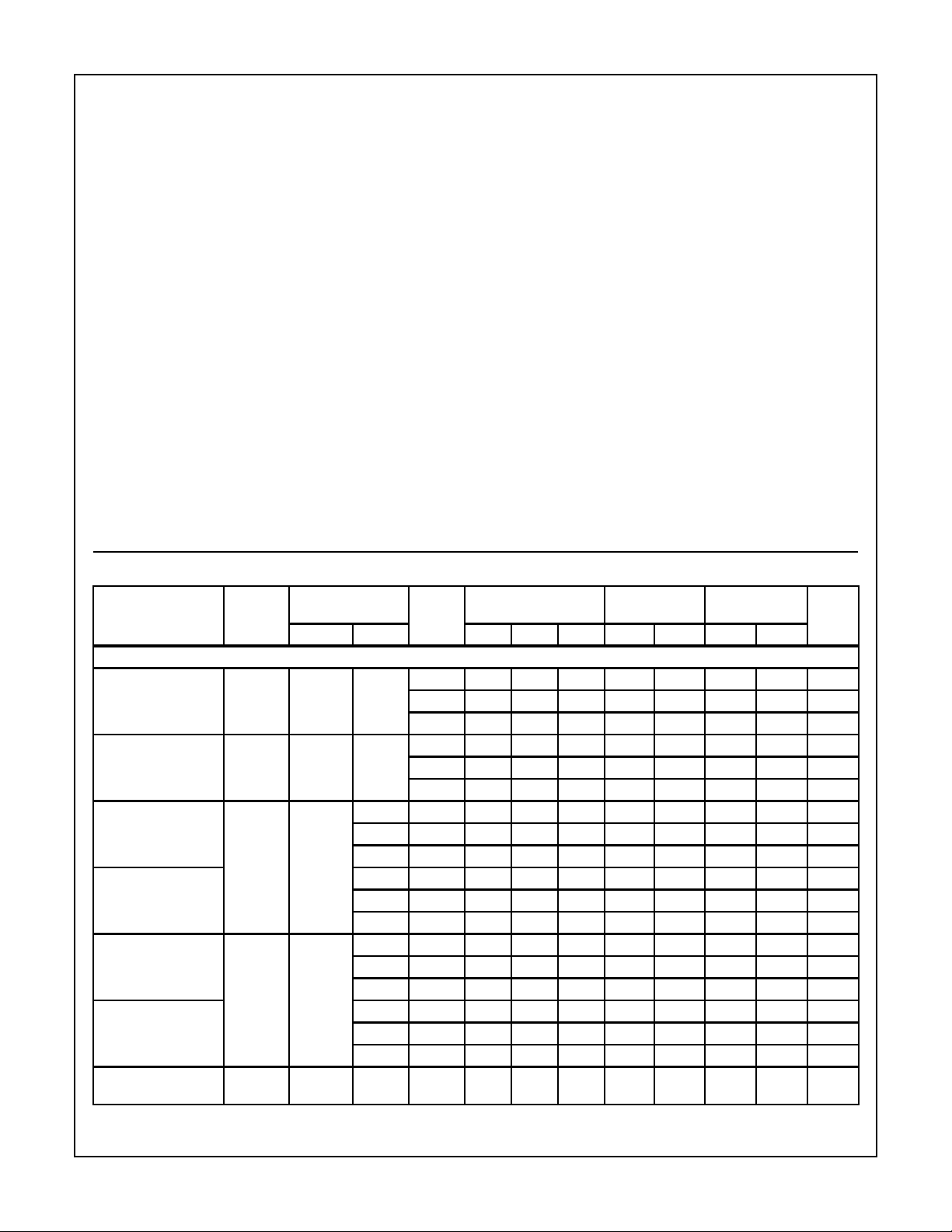
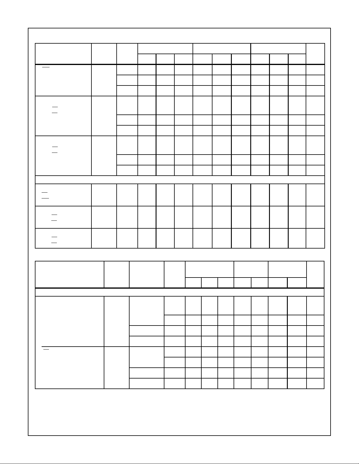
DC Electrical Specifications
PARAMETER SYMBOL
HC TYPES
High Level Input
Voltage
Low Level Input
Voltage
High Level Output
Voltage
CMOS Loads
High Level Output
Voltage
TTL Loads
Low Level Output
Voltage
CMOS Loads
Low Level Output
Voltage
TTL Loads
Input Leakage
Current
V
IH
V
IL
V
OH
V
OL
I
I
TEST
CONDITIONS
(V) IO(mA) MIN TYP MAX MIN MAX MIN MAX
I
V
CC
(V)
o
C -40oC TO 85oC -55oC TO 125oC
25
UNITSV
- - 2 1.5 - - 1.5 - 1.5 - V
4.5 3.15 - - 3.15 - 3.15 - V
6 4.2 - - 4.2 - 4.2 - V
- - 2 - - 0.5 - 0.5 - 0.5 V
4.5 - - 1.35 - 1.35 - 1.35 V
6 - - 1.8 - 1.8 - 1.8 V
VIHor VIL-0.02 2 1.9 - - 1.9 - 1.9 - V
-0.02 4.5 4.4 - - 4.4 - 4.4 - V
-0.02 6 5.9 - - 5.9 - 5.9 - V
- - ---- - - - V
-4 4.5 3.98 - - 3.84 - 3.7 - V
-5.2 6 5.48 - - 5.34 - 5.2 - V
VIHor VIL0.02 2 - - 0.1 - 0.1 - 0.1 V
0.02 4.5 - - 0.1 - 0.1 - 0.1 V
0.02 6 - - 0.1 - 0.1 - 0.1 V
- - ---- - - - V
4 4.5 - - 0.26 - 0.33 - 0.4 V
5.2 6 - - 0.26 - 0.33 - 0.4 V
VCC or
-6--±0.1 - ±1-±1 µA
GND
3
CD74HC259, CD74HCT259
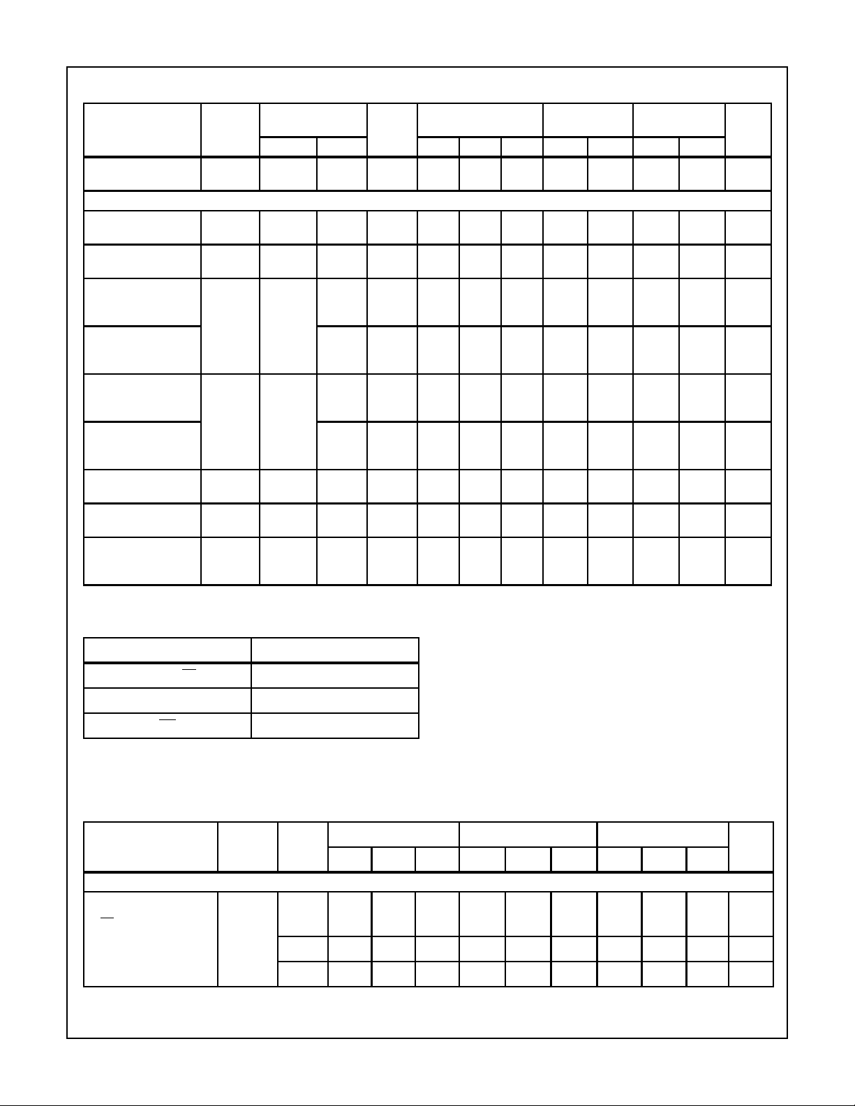
DC Electrical Specifications (Continued)
TEST
CONDITIONS
PARAMETER SYMBOL
Quiescent Device
Current
HCT TYPES
High Level Input
Voltage
Low Level Input
Voltage
High Level Output
Voltage
CMOS Loads
High Level Output
Voltage
TTL Loads
Low Level Output
Voltage
CMOS Loads
Low Level Output
Voltage
TTL Loads
Input Leakage
Current
Quiescent Device
Current
Additional Quiescent
Device Current Per
Input Pin: 1 Unit Load
NOTE: For dual-supply systems theoretical worst case (V
I
CC
V
IH
V
IL
V
OH
V
OL
I
I
I
CC
∆I
CC
(V) IO(mA) MIN TYP MAX MIN MAX MIN MAX
I
VCC or
GND
- - 4.5 to
- - 4.5 to
VIHor VIL-0.02 4.5 4.4 - - 4.4 - 4.4 - V
VIHor VIL0.02 4.5 - - 0.1 - 0.1 - 0.1 V
VCCand
GND
VCC or
GND
V
CC
-2.1
0 6 - - 8 - 80 - 160 µA
-4 4.5 3.98 - - 3.84 - 3.7 - V
4 4.5 - - 0.26 - 0.33 - 0.4 V
0 5.5 - ±0.1 - ±1-±1 µA
0 5.5 - - 8 - 80 - 160 µA
- 4.5 to
o
C -40oC TO 85oC -55oC TO 125oC
V
CC
(V)
5.5
5.5
5.5
= 2.4V, VCC = 5.5V) specification is 1.8mA.
I
25
2--2- 2 - V
- - 0.8 - 0.8 - 0.8 V
- 100 360 - 450 - 490 µA
UNITSV
HCT Input Loading Table
INPUT UNIT LOADS
A0 - A2, LE 1.5
D 1.2
MR 0.75
NOTE: Unit Load is ∆ICClimit specified in DC Electrical Table,e.g.,
360µA max at 25oC.
Prerequisite for Switching Specifications
25oC -40oC TO 85oC -55oC TO 125oC
PARAMETER SYMBOL VCC(V)
HC TYPES
Pulse Width t
LE 2 70 - - 90 - - 105 - - ns
WL
4.5 14 - - 18 - - 21 - - ns
612--15- -18--ns
UNITSMIN TYP MAX MIN TYP MAX MIN TYP MAX
4
CD74HC259, CD74HCT259
Prerequisite for Switching Specifications (Continued)
25oC -40oC TO 85oC -55oC TO 125oC
PARAMETER SYMBOL VCC(V)
MR t
Setup Time t
D to LE
A to LE
Hold Time t
D to LE
A to LE
HCT TYPES
Pulse Width
LE
MR
Setup Time
D to LE
A to LE
t
t
WL
SU
H
WL
SU
UNITSMIN TYP MAX MIN TYP MAX MIN TYP MAX
2 70 - - 90 - - 105 - - ns
4.5 14 - - 18 - - 21 - - ns
612--15- -18--ns
2 80 - - 100 - - 120 - - ns
4.5 16 - - 20 - - 24 - - ns
614--17- -20--ns
20--0--0--ns
4.5 0 - - 0 - - 0 - - ns
60--0--0--ns
4.5 18 - - 23 - - 27 - - ns
4.5 17 - - 21 - - 26 - - ns
Hold Time
D to LE
A to LE
Switching Specifications C
PARAMETER SYMBOL
HC TYPES
Propagation Delay t
D to Q 2 - - 185 - 230 - 280 ns
LE to Q t
t
H
4.5 0 - - 0 - - 0 - - ns
= 50pF, Input tr, tf= 6ns
L
CONDITIONS VCC(V)
PHL
PHL
CL = 50pF
CL = 15pF 5 - 15 - - - - - ns
CL = 50pF 6 - - 31 - 39 - 48 ns
CL = 50pF 2 - - 170 - 215 - 255 ns
CL = 15pF 5 - 14 - - - - - ns
CL = 50pF 6 - - 29 - 37 - 43 ns
TEST
-40oC TO
25oC
4.5 - - 37 - 46 - 56 ns
4.5 - - 34 - 43 - 51 ns
85oC
-55oC TO
125oC
UNITSMIN TYP MAX MIN MAX MIN MAX
5

CD74HC259, CD74HCT259
Switching Specifications C
PARAMETER SYMBOL
A to Q t
MR to Q t
Output Transition Time t
Power Dissipation Capacitance
(Notes 4, 5)
= 50pF, Input tr, tf= 6ns (Continued)
L
TEST
CONDITIONS VCC(V)
PHL
CL = 50pF 2 - - 185 - 230 - 280 ns
4.5 - - 37 - 46 - 56 ns
CL = 15pF 5 - 15 - - - - - ns
CL = 50pF 6 - - 31 - 39 - 48 ns
PHL,tPLHCL
= 50pF 2 - - 155 - 195 - 235 ns
4.5 - - 31 - 39 - 47 ns
CL = 15pF 5 - 13 - - - - - ns
CL = 50pF 6 - - 26 - 33 - 40 ns
THL
, t
CL = 50pF 2 - - 75 - 95 - 110 ns
TLH
4.5 - - 15 - 19 - 22 ns
6 - - 13 - 16 - 19 ns
C
PD
CL = 15pF 5 - 21 - - - - - pF
25oC
-40oC TO
85oC
-55oC TO
125oC
UNITSMIN TYP MAX MIN MAX MIN MAX
Input Capacitance C
I
CL = 50pF - 10 - 10 - 10 - 10 pF
HCT TYPES
Propagation Delay t
PHL,tPLH
D to Q CL = 50pF 4.5 - - 39 - 49 - 59 ns
CL = 15pF 5 - 16 - - - - - ns
LE to Q CL = 50pF 4.5 - - 38 - 48 - 57 ns
CL = 15pF 5 - 16 - - - - - ns
A to Q CL = 50pF 4.5 - - 41 - 51 - 61 ns
CL = 15pF 5 - 17 - - - - - ns
MR to Q CL = 50pF 4.5 - - 39 - 49 - 59 ns
CL = 15pF 5 - 16 - - - - - ns
Power Dissipation Capacitance
C
PD
CL = 15pF 5 - 22 - - - - - pF
(Notes 4, 5)
Input Capacitance C
Output Transition Time t
THL
I
, t
CL = 50pF - 10 - 10 - 10 - 10 pF
CL = 50pF 4.5 - - 15 - 19 - 22 ns
TLH
NOTES:
4. CPD is used to determine the dynamic power consumption, per package.
5. PD=CPDV
CC
2
fi+ ∑ CLV
2
fOwhere fi= Input Frequency, fO= Output Frequency, CL= Output Load Capacitance,
CC
VCC = Supply Voltage.
6

Test Circuits and Waveforms
trC
L
CLOCK
10%
90%
50%
10%
tfC
t
L
WL
tWL+ tWH=
50%
t
CD74HC259, CD74HCT259
WH
fC
50%
I
L
V
CC
GND
trCL= 6ns
CLOCK
0.3V
2.7V
1.3V
0.3V
t
fCL
t
WL
= 6ns
1.3V
t
WH
t
WL
+ tWH=
1.3V
I
fC
L
3V
GND
NOTE: Outputs should be switching from 10% VCC to 90% VCC in
accordance with device truth table.For f
, input duty cycle = 50%.
MAX
FIGURE 1. HC CLOCK PULSE RISE AND FALL TIMES AND
PULSE WIDTH
tr = 6ns tf = 6ns
V
t
TLH
CC
GND
INPUT
t
90%
50%
10%
THL
90%
t
50%
10%
PLH
INVERTING
OUTPUT
t
PHL
FIGURE 3. HCTRANSITION TIMES AND PROPAGATION
DELAY TIMES, COMBINATION LOGIC
tfC
L
V
CC
50%
GND
t
H(L)
V
CC
50%
t
SU(L)
GND
CLOCK
INPUT
DAT A
INPUT
t
SU(H)
trC
L
90%
10%
t
H(H)
NOTE: Outputs should be switching from 10% VCC to 90% VCC in
accordance with device truth table.For f
, input duty cycle = 50%.
MAX
FIGURE 2. HCT CLOCK PULSE RISE AND FALL TIMES AND
PULSE WIDTH
= 6ns
tr = 6ns
INPUT
t
2.7V
1.3V
0.3V
THL
t
f
3V
GND
t
TLH
90%
t
PLH
1.3V
10%
INVERTING
OUTPUT
t
PHL
FIGURE 4. HCTTRANSITION TIMES AND PROPAGATION
DELAY TIMES, COMBINATION LOGIC
CLOCK
INPUT
DAT A
INPUT
t
SU(H)
trC
L
2.7V
0.3V
t
H(H)
1.3V
1.3V
tfC
L
3V
1.3V
GND
t
H(L)
3V
1.3V
t
SU(L)
GND
OUTPUT
t
REM
V
CC
SET, RESET
OR PRESET
50%
90%
t
PLH
IC
t
TLH
t
THL
90%
50%
10%
t
PHL
GND
C
L
50pF
FIGURE 5. HC SETUP TIMES, HOLD TIMES, REMOVAL TIME,
AND PROPAGATION DELAY TIMES FOR EDGE
TRIGGERED SEQUENTIAL LOGIC CIRCUITS
OUTPUT
t
REM
3V
SET, RESET
1.3V
90%
1.3V
t
t
PLH
TLH
90%
1.3V
10%
t
PHL
t
THL
OR PRESET
IC
C
L
50pF
FIGURE 6. HCT SETUP TIMES, HOLD TIMES, REMOVAL TIME,
AND PROPAGATION DELAY TIMES FOR EDGE
TRIGGERED SEQUENTIAL LOGIC CIRCUITS
7
GND

CD74HC259, CD74HCT259
Test Circuits and Waveforms
6ns 6ns
OUTPUT
DISABLE
OUTPUT LOW
TO OFF
OUTPUT HIGH
TO OFF
50%
t
t
OUTPUTS
ENABLED
PLZ
PHZ
90%
10%
90%
OUTPUTS
DISABLED
(Continued)
10%
t
PZL
t
PZH
FIGURE 7. HCTHREE-STATE PROPAGATION DELAY
WAVEFORM
OTHER
INPUTS
TIED HIGH
OR LOW
OUTPUT
DISABLE
50%
50%
OUTPUTS
ENABLED
IC WITH
THREE-
STATE
OUTPUT
V
CC
GND
OUTPUT
R
t
r
OUTPUT
DISABLE
OUTPUT LOW
TO OFF
OUTPUT HIGH
TO OFF
t
t
OUTPUTS
ENABLED
6ns t
PLZ
PHZ
10%
90%
f
2.7
1.3
OUTPUTS
DISABLED
0.3
t
t
6ns
PZL
PZH
FIGURE 8. HCTTHREE-STATE PROPAGATION DELAY
WAVEFORM
= 1kΩ
L
C
L
50pF
VCC FOR t
GND FOR t
PLZ
PHZ
AND t
AND t
PZL
PZH
3V
GND
1.3V
1.3V
OUTPUTS
ENABLED
NOTE: Opendrain waveforms t
VCC, CL = 50pF.
FIGURE 9. HC AND HCT THREE-STATE PROPAGATION DELAY TEST CIRCUIT
PLZ
and t
are the same as those for three-state shown on the left. The test circuit is Output RL=1kΩ to
PZL
8

IMPORTANT NOTICE
T exas Instruments and its subsidiaries (TI) reserve the right to make changes to their products or to discontinue
any product or service without notice, and advise customers to obtain the latest version of relevant information
to verify, before placing orders, that information being relied on is current and complete. All products are sold
subject to the terms and conditions of sale supplied at the time of order acknowledgement, including those
pertaining to warranty, patent infringement, and limitation of liability.
TI warrants performance of its semiconductor products to the specifications applicable at the time of sale in
accordance with TI’s standard warranty. Testing and other quality control techniques are utilized to the extent
TI deems necessary to support this warranty . Specific testing of all parameters of each device is not necessarily
performed, except those mandated by government requirements.
CERTAIN APPLICATIONS USING SEMICONDUCTOR PRODUCTS MAY INVOLVE POTENTIAL RISKS OF
DEATH, PERSONAL INJURY, OR SEVERE PROPERTY OR ENVIRONMENTAL DAMAGE (“CRITICAL
APPLICATIONS”). TI SEMICONDUCTOR PRODUCTS ARE NOT DESIGNED, AUTHORIZED, OR
WARRANTED TO BE SUITABLE FOR USE IN LIFE-SUPPORT DEVICES OR SYSTEMS OR OTHER
CRITICAL APPLICA TIONS. INCLUSION OF TI PRODUCTS IN SUCH APPLICATIONS IS UNDERST OOD TO
BE FULLY AT THE CUSTOMER’S RISK.
In order to minimize risks associated with the customer’s applications, adequate design and operating
safeguards must be provided by the customer to minimize inherent or procedural hazards.
TI assumes no liability for applications assistance or customer product design. TI does not warrant or represent
that any license, either express or implied, is granted under any patent right, copyright, mask work right, or other
intellectual property right of TI covering or relating to any combination, machine, or process in which such
semiconductor products or services might be or are used. TI’s publication of information regarding any third
party’s products or services does not constitute TI’s approval, warranty or endorsement thereof.
Copyright 1998, Texas Instruments Incorporated
 Loading...