

Texas Instruments CD74HCT237E, CD74HCT137M96, CD74HCT137E, CD74HC237M96, CD74HC237M Datasheet
...
CD74HC137, CD74HCT137,
/
j
[ /Title
(CD74
HC137
,
CD74
HCT13
7,
CD74
HC237
,
CD74
HCT23
7)
Subect
(High
Speed
Data sheet acquired from Harris Semiconductor
SCHS146
March 1998
Features
• Select One of Eight Data Outputs
- Active Low for CD74HC137 and CD74HCT137
- Active High for CD74HC237 and CD74HCT237
• l/O Port or Memory Selector
• Two Enable Inputs to Simplify Cascading
• Typical Propagation Delay of 13ns at V
15pF, T
= 25oC (CD74HC237)
A
• Fanout (Over Temperature Range)
- Standard Outputs. . . . . . . . . . . . . . . 10 LSTTL Loads
- Bus Driver Outputs . . . . . . . . . . . . . 15 LSTTL Loads
• Wide Operating Temperature Range . . . -55
• Balanced Propagation Delay and Transition Times
• Significant Power Reduction Compared to LSTTL
Logic ICs
• HC Types
- 2V to 6V Operation
- High Noise Immunity: N
= 30%, NIH = 30%, of V
IL
at VCC = 5V
CC
= 5V,
o
CD74HC237, CD74HCT237
High Speed CMOS Logic, 3-to-8 Line Decoder
Demultiplexer with Address Latches
C to 125oC
CC
• HCT Types
- 4.5V to 5.5V Operation
- Direct LSTTL Input Logic Compatibility,
V
= 0.8V (Max), VIH = 2V (Min)
IL
- CMOS Input Compatibility, I
≤ 1µA at VOL, V
l
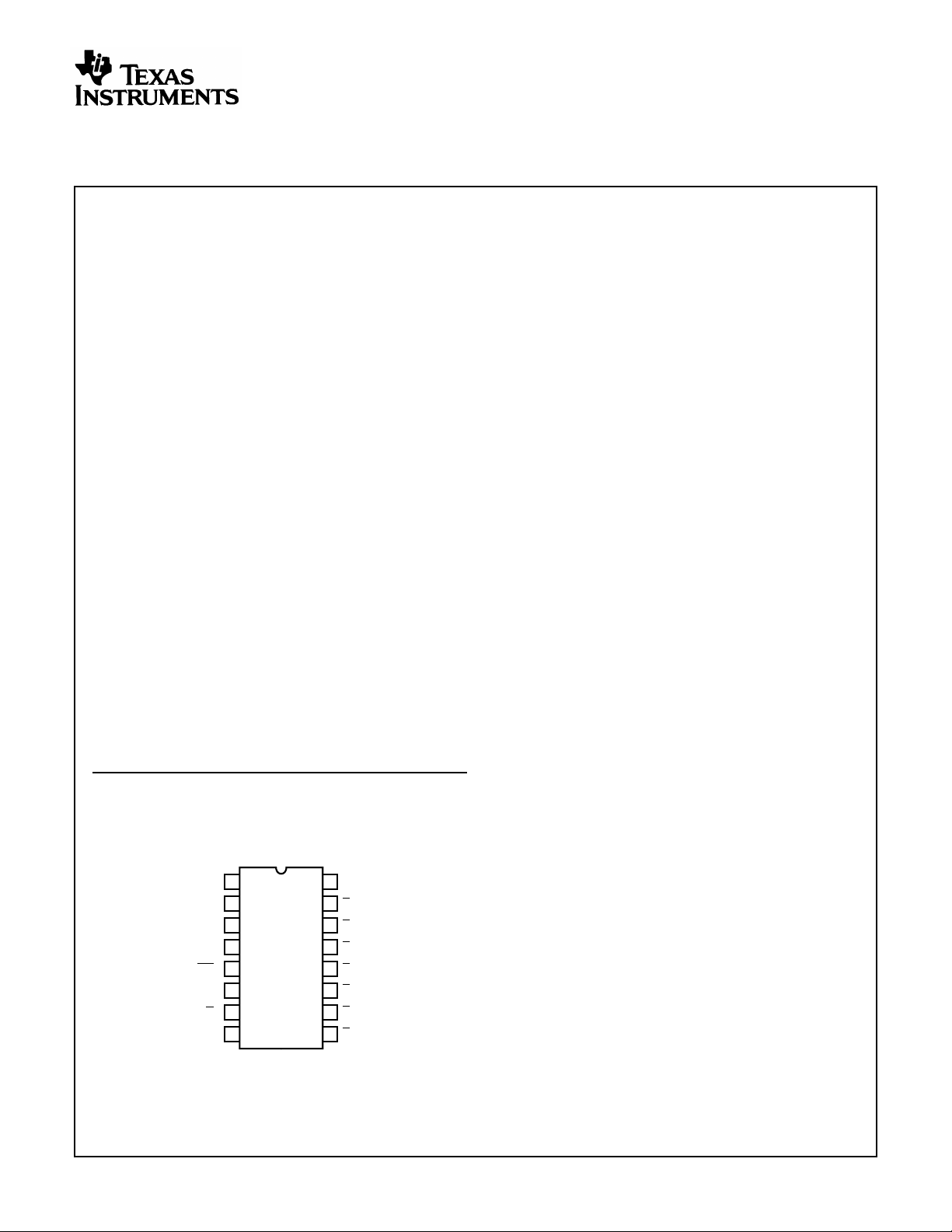
Pinout
CD74HC137, CD74HCT137, CD74HC237, CD74HCT237
(PDIP, SOIC)
TOP VIEW
16
A
A
A
LE
OE
OE
Y
GND
1
0
2
1
3
3
4
5
1
6
0
7
7
8
V
CC
15
Y
0
14
Y
1
13
Y
2
12
Y
3
11
Y
4
10
Y
5
9
Y
6
OH
CAUTION: These devices are sensitive to electrostatic discharge. Users should follow proper IC Handling Procedures.
Copyright
© Harris Corporation 1998
1
File Number 1886.1
CD74HC137, CD74HCT137, CD74HC237, CD74HCT237
Description
The Harris CD74HC137, CD74HC237 and CD74HCT137,
CD74HCT237 are high speed silicon gate CMOS decoders
well suited to memory address decoding or data routing
applications. Both circuits feature low power consumption
usually associated with CMOS circuitry, yet have speeds
comparable to low power Schottky TTL logic.
Both circuits have three binary selectinputs (A0, A1 and A2)
that can be latched by an active High Latch Enable (LE) signal to isolate the outputs from select-input changes. A “Low”
LE makes the output transparent to the input and the circuit
functions as a one-of-eight decoder. Two Output Enable
inputs (
OE1and OE0) are provided to simplify cascading
and to facilitate demultiplexing. The demultiplexing function
is accomplished by using the A
0,A1,A2
inputs to select the
desired output and using one of the other Output Enable
inputs as the data input while holding the other Output
Enable input in its active state. In the CD74HC137 and
CD74HCT137 the selected output is a “Low”; in the
CD74HC237 and CD74HCT237 the selected output is a
“High”.
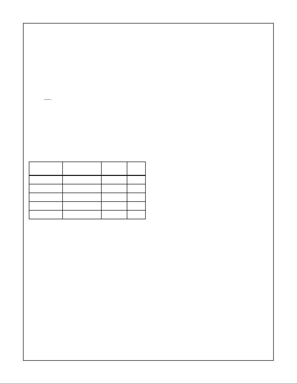
Ordering Information
PKG.
PART NUMBER TEMP. RANGE (oC) PACKAGE
CD74HC137E -55 to 125 16 Ld PDIP E16.3
CD74HCT137E -55 to 125 16 Ld PDIP E16.3
CD74HC237E -55 to 125 16 Ld PDIP E16.3
CD74HC237M -55 to 125 16 Ld SOIC M16.15
CD74HCT237E -55 to 125 16 Ld PDIP E16.3
NOTES:
1. When ordering, use the entire part number. Add the suffix 96 to
obtain the variant in the tape and reel.
2. Wafer and die for this part number is available which meets all
electrical specifications. Please contact your local sales office or
Harris customer service for ordering information.
NO.
2
CD74HC137, CD74HCT137, CD74HC237, CD74HCT237
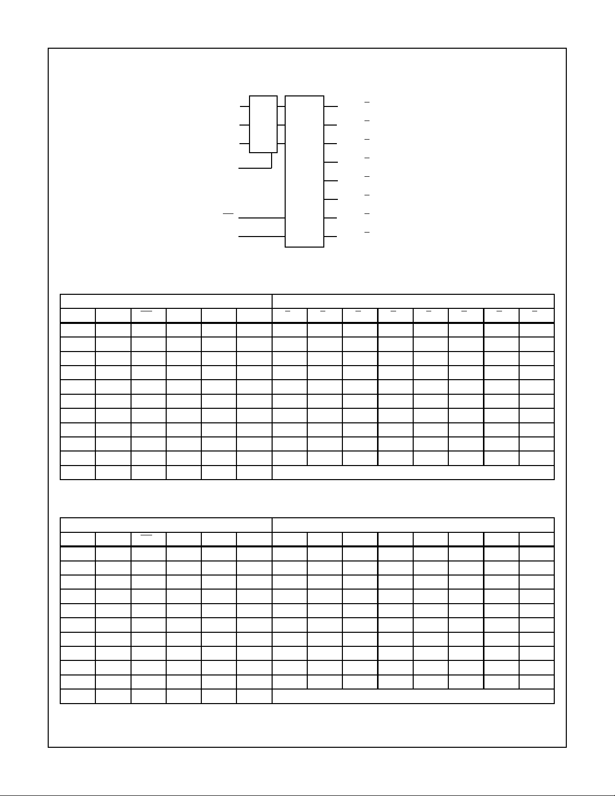
Functional Diagram
HC/HCT HC/HCT
237 137
1
A
0
2
3-BIT
A
1
OE
OE
A
LE
LATCH
3
2
4
1
0
GND = 8
V
CC
1 OF 8
DECODER
5
6
= 16
CD74HC137, CD74HCT137 TRUTH TABLE
INPUTS OUTPUTS
LE OE
OE
0
A
1
A
2
A
1
0
Y
0
XXHXXXHHHHHHHH
XLXXXXHHHHHHHH
LHLLLLLHHHHHHH
LHLLLHHLHHHHHH
LHLLHLHHLHHHHH
LHLLHHHHHLHHHH
LHLHLLHHHHLHHH
LHLHLHHHHHHLHH
LHLHHLHHHHHHLH
LHLHHHHHHHHHHL
H H L X X X Depends upon the address previously applied while LE was at a logic low.
NOTE: H = High Voltage Level, L = Low Voltage Level, X = Don’t Care
15
14
13
12
11
10
9
7
Y
1
Y
Y
0
0
Y
Y
1
1
Y
Y
2
2
Y
Y
3
3
Y
Y
4
4
Y
Y
5
5
Y
Y
6
6
Y
Y
7
7
Y
Y
2
Y
3
Y
4
Y
5
Y
6
7
CD74HC237, CD74HCT237 TRUTH TABLE
INPUTS OUTPUTS
LE OE
OE
0
A
1
A
2
A
1
0
Y
0
Y
1
Y
Y
2
Y
3
Y
4
Y
5
Y
6
XXHXXXLLLLLLLL
XLXXXXLLLLLLLL
LHLLLLHLLLLLLL
LHLLLHLHLLLLLL
LHLLHLLLHLLLLL
LHLLHHLLLHLLLL
LHLHLLLLLLHLLL
LHLHLHLLLLLHLL
LHLHHLLLLLLLHL
LHLHHHLLLLLLLH
H H L X X X Depends upon the address previously applied while LE was at a logic low.
NOTE: H = High Voltage Level, L = Low Voltage Level, X = Don’t Care
3
7

CD74HC137, CD74HCT137, CD74HC237, CD74HCT237
Functional Block Diagram
LE
1
A
0
p
n
LE
LE
A
0
A
0
p
n
15
Y
0
14
Y
1
13
Y
2
OE
OE
A
A
LE
LE
A
2
1
A1 LATCH
1
A
0
12
Y
3
11
Y
4
10
A
3
2
A2 LATCH
2
A
2
Y
5
9
Y
6
LE
4
LE
7
Y
7
5
1
6
0
4

CD74HC137, CD74HCT137, CD74HC237, CD74HCT237
Absolute Maximum Ratings Thermal Information
DC Supply Voltage, VCC. . . . . . . . . . . . . . . . . . . . . . . . -0.5V to 7V
DC Input Diode Current, I
For VI < -0.5V or VI > VCC + 0.5V. . . . . . . . . . . . . . . . . . . . . .±20mA
DC Output Diode Current, I
For VO < -0.5V or VO > VCC + 0.5V . . . . . . . . . . . . . . . . . . . .±20mA
DC Output Source or Sink Current per Output Pin, I
For VO > -0.5V or VO < VCC + 0.5V . . . . . . . . . . . . . . . . . . . .±25mA
DC VCC or Ground Current, ICC . . . . . . . . . . . . . . . . . . . . . . . . .±50mA
IK
OK
O
Operating Conditions
Temperature Range (TA) . . . . . . . . . . . . . . . . . . . . . -55oC to 125oC
Supply Voltage Range, V
HC Types . . . . . . . . . . . . . . . . . . . . . . . . . . . . . . . . . . . . .2V to 6V
HCT Types . . . . . . . . . . . . . . . . . . . . . . . . . . . . . . . . .4.5V to 5.5V
DC Input or Output Voltage, VI, VO . . . . . . . . . . . . . . . . . 0V to V
Input Rise and Fall Time
2V . . . . . . . . . . . . . . . . . . . . . . . . . . . . . . . . . . . . . . 1000ns (Max)
4.5V. . . . . . . . . . . . . . . . . . . . . . . . . . . . . . . . . . . . . . 500ns (Max)
6V . . . . . . . . . . . . . . . . . . . . . . . . . . . . . . . . . . . . . . . 400ns (Max)
CAUTION: Stresses above those listed in “Absolute Maximum Ratings” may cause permanent damage to the device. This is a stress only rating and operation
of the device at these or any other conditions above those indicated in the operational sections of this specification is not implied.
NOTE:
3. θJA is measured with the component mounted on an evaluation PC board in free air.
CC
Thermal Resistance (Typical, Note 3) θJA (oC/W)
PDIP Package. . . . . . . . . . . . . . . . . . . . . . . . . . . . . 90
SOIC Package. . . . . . . . . . . . . . . . . . . . . . . . . . . . . 160
Maximum Junction Temperature. . . . . . . . . . . . . . . . . . . . . . .150oC
Maximum Storage Temperature Range . . . . . . . . . .-65oC to 150oC
Maximum Lead Temperature (Soldering 10s). . . . . . . . . . . . .300oC
(SOIC - Lead Tips Only)
CC
DC Electrical Specifications
PARAMETER SYMBOL
HC TYPES
High Level Input
Voltage
Low Level Input
Voltage
High Level Output
Voltage
CMOS Loads
High Level Output
Voltage
TTL Loads
Low Level Output
Voltage
CMOS Loads
Low Level Output
Voltage
TTL Loads
Input Leakage
Current
V
IH
V
IL
V
OH
V
OL
I
I
TEST
CONDITIONS
- - 2 1.5 - - 1.5 - 1.5 - V
- - 2 - - 0.5 - 0.5 - 0.5 V
VIHor VIL-0.02 2 1.9 - - 1.9 - 1.9 - V
-0.02 4.5 4.4 - - 4.4 - 4.4 - V
-0.02 6 5.9 - - 5.9 - 5.9 - V
-4 4.5 3.98 - - 3.84 - 3.7 - V
-5.2 6 5.48 - - 5.34 - 5.2 - V
VIHor VIL0.02 2 - - 0.1 - 0.1 - 0.1 V
0.02 4.5 - - 0.1 - 0.1 - 0.1 V
0.02 6 - - 0.1 - 0.1 - 0.1 V
5.2 6 - - 0.26 - 0.33 - 0.4 V
VCC or
GND
V
CC
(V)
4.5 3.15 - - 3.15 - 3.15 - V
6 4.2 - - 4.2 - 4.2 - V
4.5 - - 1.35 - 1.35 - 1.35 V
6 - - 1.8 - 1.8 - 1.8 V
- - ---- - - - V
- - ---- - - - V
4 4.5 - - 0.26 - 0.33 - 0.4 V
-6--±0.1 - ±1-±1µA
25oC -40oC TO 85oC -55oCTO125oC
UNITSVI(V) IO(mA) MIN TYP MAX MIN MAX MIN MAX
5

CD74HC137, CD74HCT137, CD74HC237, CD74HCT237
DC Electrical Specifications (Continued)
TEST
CONDITIONS
PARAMETER SYMBOL
Quiescent Device
Current
HCT TYPES
High Level Input
Voltage
Low Level Input
Voltage
High Level Output
Voltage
CMOS Loads
High Level Output
Voltage
TTL Loads
Low Level Output
Voltage
CMOS Loads
Low Level Output
Voltage
TTL Loads
Input Leakage
Current
Quiescent Device
Current
Additional Quiescent
Device Current Per
Input Pin: 1 Unit Load
NOTE: For dual-supply systems theoretical worst case (VI = 2.4V, VCC = 5.5V) specification is 1.8mA.
I
CC
V
IH
V
IL
V
OH
V
OL
I
I
I
CC
∆I
CC
(Note)
VCC or
GND
- - 4.5 to
- - 4.5 to
VIHor VIL-0.02 4.5 4.4 - - 4.4 - 4.4 - V
-4 4.5 3.98 - - 3.84 - 3.7 - V
VIHor VIL0.02 4.5 - - 0.1 - 0.1 - 0.1 V
VCCand
GND
VCC or
GND
V
CC
-2.1
V
CC
(V)
0 6 - - 8 - 80 - 160 µA
5.5
5.5
4 4.5 - - 0.26 - 0.33 - 0.4 V
0 5.5 - - ±0.1 - ±1-±1µA
0 5.5 - - 8 - 80 - 160 µA
- 4.5 to
5.5
25oC -40oC TO 85oC -55oCTO125oC
2--2- 2 - V
- - 0.8 - 0.8 - 0.8 V
- 100 360 - 450 - 490 µA
UNITSVI(V) IO(mA) MIN TYP MAX MIN MAX MIN MAX
HCT Input Loading Table
INPUT UNIT LOADS
All 1.5
NOTE: Unit Load is ∆ICClimit specified in DC Electrical Table,e.g.,
360µA max at 25oC.
Prerequisite For Switching Specifications
V
PARAMETER SYMBOL
HC TYPES
Anto LE Setup Time t
An to LE Hold Time t
SU
H
CC
(V)
250- -65-75-ns
4.5 10 - - 13 - 15 - ns
6 9 - - 11 - 13 - ns
230- -40-45-ns
4.56--8-9-ns
65--7-8-ns
25oC -40oC TO 85oC -55oCTO125oC
UNITSMIN TYP MAX MIN MAX MIN MAX
6

CD74HC137, CD74HCT137, CD74HC237, CD74HCT237
Prerequisite For Switching Specifications (Continued)
V
PARAMETER SYMBOL
LE Pulse Width t
W
CC
(V)
250- -65-75-ns
4.5 10 - - 13 - 15 - ns
6 9 - - 1 - 13 - ns
HCT TYPES
An to LE Setup Time t
SU
4.5 10 - - 13 - 15 - ns
An to LE Hold Time
t
CD74HCT137 4.5 7 - - 9 - 11 - ns
CD74HCT237 t
LE Pulse Width t
H
H
W
4.55--5-5-ns
4.5 10 - - 13 - 15 - ns
25oC -40oC TO 85oC -55oCTO125oC
UNITSMIN TYP MAX MIN MAX MIN MAX
Switching Specifications Input t
, tf = 6ns
r
-40oC TO
PARAMETER SYMBOL
TEST
CONDITIONS V
CC
25oC
(V)
85oC -55oC TO 125oC
HC TYPES
Propagation Delay
t
PLH,tPHLCL
= 50pF 2 - - 180 - 225 - 270 ns
CD74HC137, CD74HCT137
An to any Y 4.5 - - 36 - 45 - 54 ns
6 - - 31 - 38 - 46 ns
Propagation Delay
t
PLH,tPHLCL
= 50pF 2 - - 160 - 200 - 240 ns
CD74HC237, CD74HCT237
An to any Y 4.5 - - 32 - 40 - 48 ns
6 - - 27 - 34 - 41 ns
Address to Output
CD74HC137 t
CD74HC237 t
OE0 to any Y or Y t
, t
PLH
PHLCL
, t
PLH
PHLCL
PLH,tPHLCL
= 15pF 5 5 15 - - - - - ns
= 15pF 5 - 13 - - - - - ns
= 50pF 2 - - 145 - 180 - 220 ns
4.5 - - 29 - 36 - 44 ns
6 - - 25 - 31 - 38 ns
OE1 to any Y or Y t
TLH
, t
THLCL
= 50pF 2 - - 145 - 180 - 220 ns
4.5 - - 29 - 36 - 44 ns
6 - - 25 - 31 - 38 ns
LE to any Y or Y t
TLH
, t
THLCL
= 50pF 2 - - 190 - 240 - 285 ns
4.5 - - 38 - 48 - 57 ns
6 - - 32 - 41 - 48 ns
Power Dissipation
Capacitance, (Notes 4, 5)
CD74HC137 C
CD74HC237 C
Output Transition Time t
TLH
CL = 15pF 5 - 19 - - - - - pF
PD
CL = 15pF 5 - 23 - - - - - pF
PD
, t
THLCL
= 50pF 2 - - 75 - 95 - 110 ns
4.5 - - 15 - 19 - 22 ns
6 - - 13 - 16 - 19 ns
Input Capacitance C
I
- - - - 10 - 10 - 10 pF
UNITSMIN TYP MAX MIN MAX MIN MAX
7

CD74HC137, CD74HCT137, CD74HC237, CD74HCT237
Switching Specifications Input t
, tf = 6ns (Continued)
r
TEST
PARAMETER SYMBOL
CONDITIONS V
CC
(V)
HCT TYPES
Propagation Delay
An to any Y or Y
Address to Output
OE0to any Y (HC137) t
OE0to any Y (HC237) t
OE1to any Y (HC137) t
OE1to any Y (HC237) t
LE to any Y (HC137) t
LE to any Y (HC237) t
t
PLH
t
PLH
PLH
PLH
TLH
TLH
TLH
TLH
, t
PHLCL
, t
PHLCL
, t
PHLCL
, t
PHLCL
, t
THLCL
, t
THLCL
, t
THL
, t
THLCL
= 50pF 4.5 - - 38 - 48 - 57 ns
= 15pF 5 - 16 - - - - - ns
= 50pF 4.5 - - 35 - 44 - 53 ns
= 50pF 4.5 - - 33 - 41 - 60 ns
= 50pF 4.5 - - 37 - 46 - 56 ns
= 50pF 4.5 - - 35 - 44 - 53 ns
CL = 50pF 4.5 - - 44 - 55 - 66 ns
= 50pF 4.5 - - 42 - 53 - 63 ns
Power Dissipation
Capacitance, (Notes 4, 5)
CD74HC137 C
CD74HC237 C
Output Transition Time t
TLH
Input Capacitance C
CL = 15pF 5 - 19 - - - - - pF
PD
CL= 15pF 5 - 23 - - - - - pF
PD
, t
THLCL
I
= 50pF 4.5 15 19 22 ns
- - - - 10 - 10 - 10 pF
NOTES:
4. CPD is used to determine the dynamic power consumption, per gate.
5. PD = V
2
fi(CPD + CL) where: fi = Input Frequency, CL = Output Load Capacitance, VCC = Supply Voltage.
CC
25oC
-40oC TO
85oC -55oC TO 125oC
UNITSMIN TYP MAX MIN MAX MIN MAX
Test Circuits and Waveforms
t
TLH
I
fC
50%
V
CC
GND
L
V
CC
GND
trC
L
CLOCK
10%
90%
50%
10%
tfC
t
L
WL
tWL+ tWH=
50%
t
WH
NOTE: Outputs should be switching from 10% VCC to 90% VCC in
accordance with device truth table.For f
, input duty cycle = 50%.
MAX
FIGURE 1. HC CLOCK PULSE RISE AND FALL TIMES AND
PULSE WIDTH
tr = 6ns tf = 6ns
t
PHL
90%
50%
10%
t
90%
50%
10%
PLH
INPUT
INVERTING
OUTPUT
t
THL
1.3V
I
fC
L
3V
GND
t
rCL
CLOCK
= 6ns
0.3V
2.7V
1.3V
0.3V
+ tWH=
t
t
WL
WH
= 6ns
t
fCL
1.3V
t
WL
NOTE: Outputs should be switching from 10% VCC to 90% VCC in
accordance with device truth table.For f
, input duty cycle = 50%.
MAX
FIGURE 2. HCT CLOCK PULSE RISE AND FALL TIMES AND
PULSE WIDTH
= 6ns
t
PLH
t
f
1.3V
10%
90%
t
3V
GND
TLH
tr = 6ns
INPUT
t
INVERTING
OUTPUT
THL
t
2.7V
1.3V
0.3V
PHL
FIGURE 3. HC AND HCU TRANSITION TIMES AND PROPAGA-
TION DELAY TIMES, COMBINATION LOGIC
FIGURE 4. HCT TRANSITION TIMES AND PROPAGATION
DELAY TIMES, COMBINATION LOGIC
8

Test Circuits and Waveforms
(Continued)
90%
t
PLH
IC
t
TLH
tfC
L
V
CC
50%
GND
t
H(L)
V
CC
50%
t
SU(L)
90%
t
THL
GND
50%
10%
t
PHL
GND
C
L
CLOCK
INPUT
DAT A
INPUT
t
SU(H)
OUTPUT
t
REM
V
CC
SET, RESET
OR PRESET
trC
L
90%
10%
t
H(H)
50%
50pF
FIGURE 5. HC SETUP TIMES, HOLD TIMES, REMOVAL TIME,
AND PROPAGATION DELAY TIMES FOR EDGE
TRIGGERED SEQUENTIAL LOGIC CIRCUITS
CLOCK
INPUT
DAT A
INPUT
t
SU(H)
OUTPUT
t
REM
3V
SET, RESET
OR PRESET
trC
L
2.7V
0.3V
t
H(H)
1.3V
1.3V
1.3V
90%
t
PLH
IC
1.3V
t
TLH
tfC
L
3V
1.3V
GND
t
H(L)
3V
1.3V
t
SU(L)
90%
1.3V
10%
t
t
PHL
THL
GND
GND
C
L
50pF
FIGURE 6. HCT SETUP TIMES, HOLD TIMES, REMOVALTIME,
AND PROPAGATION DELAY TIMES FOR EDGE
TRIGGERED SEQUENTIAL LOGIC CIRCUITS
9

IMPORTANT NOTICE
T exas Instruments and its subsidiaries (TI) reserve the right to make changes to their products or to discontinue
any product or service without notice, and advise customers to obtain the latest version of relevant information
to verify, before placing orders, that information being relied on is current and complete. All products are sold
subject to the terms and conditions of sale supplied at the time of order acknowledgement, including those
pertaining to warranty, patent infringement, and limitation of liability.
TI warrants performance of its semiconductor products to the specifications applicable at the time of sale in
accordance with TI’s standard warranty. Testing and other quality control techniques are utilized to the extent
TI deems necessary to support this warranty . Specific testing of all parameters of each device is not necessarily
performed, except those mandated by government requirements.
CERT AIN APPLICATIONS USING SEMICONDUCT OR PRODUCTS MAY INVOLVE POTENTIAL RISKS OF
DEATH, PERSONAL INJURY, OR SEVERE PROPERTY OR ENVIRONMENTAL DAMAGE (“CRITICAL
APPLICATIONS”). TI SEMICONDUCTOR PRODUCTS ARE NOT DESIGNED, AUTHORIZED, OR
WARRANTED TO BE SUITABLE FOR USE IN LIFE-SUPPORT DEVICES OR SYSTEMS OR OTHER
CRITICAL APPLICA TIONS. INCLUSION OF TI PRODUCTS IN SUCH APPLICATIONS IS UNDERST OOD TO
BE FULLY AT THE CUSTOMER’S RISK.
In order to minimize risks associated with the customer’s applications, adequate design and operating
safeguards must be provided by the customer to minimize inherent or procedural hazards.
TI assumes no liability for applications assistance or customer product design. TI does not warrant or represent
that any license, either express or implied, is granted under any patent right, copyright, mask work right, or other
intellectual property right of TI covering or relating to any combination, machine, or process in which such
semiconductor products or services might be or are used. TI’s publication of information regarding any third
party’s products or services does not constitute TI’s approval, warranty or endorsement thereof.
Copyright 1999, Texas Instruments Incorporated
 Loading...