

Texas Instruments CD74HCT193E, CD74HC193M96, CD74HC193M, CD74HC193E, CD74HC192E Datasheet
...
1
Data sheet acquired from Harris Semiconductor
SCHS163
Features
• Synchronous Counting and Asynchronous
Loading
• Two Outputs for N-Bit Cascading
• Look-Ahead Carry for High-Speed Counting
• Fanout (Over Temperature Range)
- Standard Outputs. . . . . . . . . . . . . . . 10 LSTTL Loads
- Bus Driver Outputs . . . . . . . . . . . . . 15 LSTTL Loads
• Wide Operating Temperature Range . . . -55
o
C to 125oC
• Balanced Propagation Delay and Transition Times
• Significant Power Reduction Compared to LSTTL
Logic ICs
• HC Types
- 2V to 6V Operation
- High Noise Immunity: N
IL
= 30%, NIH = 30% of V
CC
at VCC = 5V
• HCT Types
- 4.5V to 5.5V Operation
- Direct LSTTL Input Logic Compatibility,
V
IL
= 0.8V (Max), VIH = 2V (Min)
- CMOS Input Compatibility, I
l
≤ 1µA at VOL, V
OH
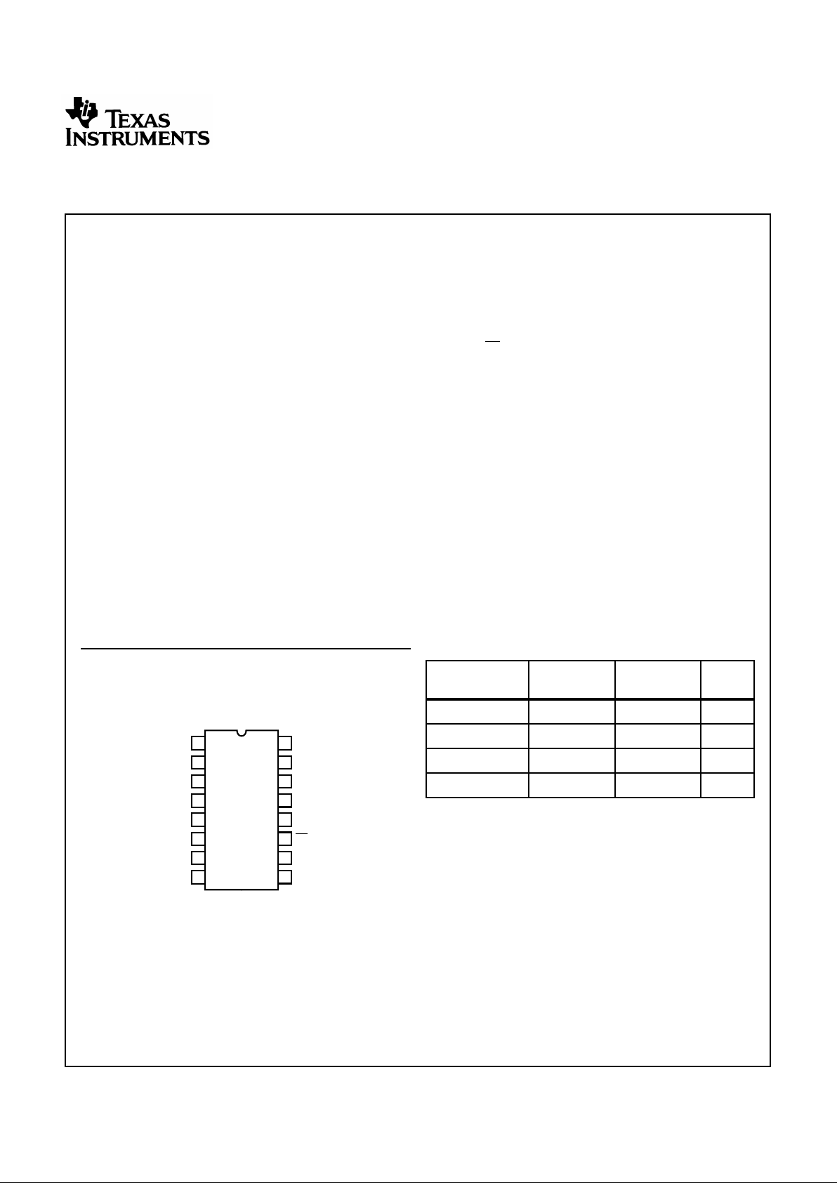
Pinout
CD74HC192, CD74HC193, CD74HCT193
(PDIP, SOIC)
TOP VIEW
Description
The Harris CD74HC192, CD74HC193and CD74HCT193 are
asynchronously presettable BCD Decade and Binary
Up/Down synchronous counters, respectively.
Presetting thecounter to the number on the preset data inputs
(P0-P3) is accomplished by a LOW asynchronous parallel
load input (
PL). The counter is incremented on the low-to-high
transition of the Clock-Up input (and a high level on the ClockDown input) and decremented on the low to high transition of
the Clock-Down input (and a high level on the Clock-up input).
A high level on the MR input overrides any other input to clear
the counter to its zero state. The Terminal Count up (carry)
goes low half a clock period before the zero count is reached
and returns to a high level at the zero count. The Terminal
Count Down (borrow) in the count down mode likewise goes
low half a clock period before the maximum count (9 in the
192 and 15 in the 193) and returns to high at the maximum
count. Cascading is effected by connecting the carry and
borrow outputs of a less significant counter to the Clock-Up
and CLock-Down inputs, respectively, of the next most
significant counter.
If a decade counter is present to an illegal state or assumes
an illegal state when power is applied, it will return to the
normal sequence in one count as shown in state diagram.
14
15
16
9
13
12
11
10
1
2
3
4
5
7
6
8
P1
Q1
Q0
CPD
CPU
Q2
GND
Q3
V
CC
MR
TCD
TCU
PL
P2
P3
P0
Ordering Information
PART NUMBER
TEMP.RANGE
(oC) PACKAGE
PKG.
NO.
CD74HC192E -55 to 125 16 Ld PDIP E16.3
CD74HC193E -55 to 125 16 Ld PDIP E16.3
CD74HCT193E -55 to 125 16 Ld PDIP E16.3
CD74HCT193M -55 to 125 16 Ld SOIC M16.15
NOTES:
1. When ordering, use the entire part number. Add the suffix 96 to
obtain the variant in the tape and reel.
2. Wafer or diefor this partnumber is availablewhich meets allelectrical specifications. Please contact your local sales office or
Harris customer service for ordering information.
September 1997
CAUTION: These devices are sensitive to electrostatic discharge. Users should follow proper IC Handling Procedures.
Copyright
© Harris Corporation 1997
File Number 1674.1
CD74HC192, CD74HC193,
CD74HCT193
High Speed CMOS Logic
Presettable Synchronous 4-Bit Up/Down Counters
[ /Title
(CD74
HC192
,
CD74
HC193
,
CD74
HCT19
3)
/
Sub-
j
ect
(High
Speed
CMOS
Logic
Preset-
2
Functional Diagram
TRUTH TABLE
CLOCK UP
CLOCK
DOWN RESET
PARALLEL
LOAD FUNCTION
↑ H L H Count Up
H ↑ L H Count Down
X X H X Reset
X X L L Load Preset Inputs
NOTE: H = High Voltage Level, L = Low Voltage Level, X = Don’t Care, ↑ = Transition from
Low to High Level
ASYN.
MASTER
CLOCK UP
11
14
5
4
15 1 10 9
3
6
7
12
13
Q
0
Q
1
Q
2
Q
3
TERMINAL
P0 P1 P2 P3
LOAD
CLOCK DOWN
2
TERMINAL
COUNT UP
BCD (192)
BINARY (193)
OUTPUTS
BCD/BINARY
PRESET
ENABLE
PARALLEL
PL
RESET
COUNT DOWN
CD74HC192, CD74HC193, CD74HCT193
3
Absolute Maximum Ratings Thermal Information
DC Supply Voltage, VCC. . . . . . . . . . . . . . . . . . . . . . . . -0.5V to 7V
DC Input Diode Current, I
IK
For VI < -0.5V or VI > VCC + 0.5V. . . . . . . . . . . . . . . . . . . . . .±20mA
DC Output Diode Current, I
OK
For VO < -0.5V or VO > VCC + 0.5V . . . . . . . . . . . . . . . . . . . .±20mA
DC Output Source or Sink Current per Output Pin, I
O
For VO > -0.5V or VO < VCC + 0.5V . . . . . . . . . . . . . . . . . . . .±25mA
DC VCC or Ground Current, I
CC orIGND
. . . . . . . . . . . . . . . . . .±50mA
Operating Conditions
Temperature Range (TA) . . . . . . . . . . . . . . . . . . . . . -55oC to 125oC
Supply Voltage Range, V
CC
HC Types . . . . . . . . . . . . . . . . . . . . . . . . . . . . . . . . . . . . .2V to 6V
HCT Types . . . . . . . . . . . . . . . . . . . . . . . . . . . . . . . . .4.5V to 5.5V
DC Input or Output Voltage, VI, VO . . . . . . . . . . . . . . . . . 0V to V
CC
Input Rise and Fall Time
2V . . . . . . . . . . . . . . . . . . . . . . . . . . . . . . . . . . . . . . 1000ns (Max)
4.5V. . . . . . . . . . . . . . . . . . . . . . . . . . . . . . . . . . . . . . 500ns (Max)
6V . . . . . . . . . . . . . . . . . . . . . . . . . . . . . . . . . . . . . . . 400ns (Max)
Thermal Resistance (Typical, Note 3) θJA (oC/W)
PDIP Package. . . . . . . . . . . . . . . . . . . . . . . . . . . . . 90
SOIC Package. . . . . . . . . . . . . . . . . . . . . . . . . . . . . 160
Maximum Junction Temperature. . . . . . . . . . . . . . . . . . . . . . .150oC
Maximum Storage Temperature Range . . . . . . . . . .-65oC to 150oC
Maximum Lead Temperature (Soldering 10s). . . . . . . . . . . . .300oC
(SOIC - Lead Tips Only)
CAUTION: Stresses above those listed in “Absolute Maximum Ratings” may cause permanent damage to the device. This is a stress only rating and operation
of the device at these or any other conditions above those indicated in the operational sections of this specification is not implied.
NOTE:
3. θJA is measured with the component mounted on an evaluation PC board in free air.
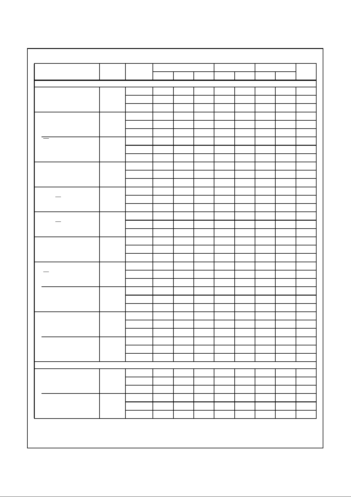
DC Electrical Specifications
PARAMETER SYMBOL
TEST
CONDITIONS 25oC -40oC TO 85oC -55oC TO 125oC
UNITSVI(V) IO(mA) VCC (V) MIN TYP MAX MIN MAX MIN MAX
HC TYPES
High Level Input
Voltage
V
IH
- - 2 1.5 - - 1.5 - 1.5 - V
4.5 3.15 - - 3.15 - 3.15 - V
6 4.2 - - 4.2 - 4.2 - V
Low Level Input
Voltage
V
IL
- - 2 - - 0.5 - 0.5 - 0.5 V
4.5 - - 1.35 - 1.35 - 1.35 V
6 - - 1.8 - 1.8 - 1.8 V
High Level Output
Voltage
CMOS Loads
V
OH
VIH or
V
IL
-0.02 2 1.9 - - 1.9 - 1.9 - V
-0.02 4.5 4.4 - - 4.4 - 4.4 - V
-0.02 6 5.9 - - 5.9 - 5.9 - V
High Level Output
Voltage
TTL Loads
-4 4.5 3.98 - - 3.84 - 3.7 - V
-5.2 6 5.48 - - 5.34 - 5.2 - V
Low Level Output
Voltage
CMOS Loads
V
OL
VIH or
V
IL
0.02 2 - - 0.1 - 0.1 - 0.1 V
0.02 4.5 - - 0.1 - 0.1 - 0.1 V
0.02 6 - - 0.1 - 0.1 - 0.1 V
Low Level Output
Voltage
TTL Loads
4 4.5 - - 0.26 - 0.33 - 0.4 V
5.2 6 - - 0.26 - 0.33 - 0.4 V
Input Leakage
Current
I
I
VCC or
GND
-6--±0.1 - ±1-±1 µA
Quiescent Device
Current
I
CC
VCC or
GND
0 6 - - 8 - 80 - 160 µA
CD74HC192, CD74HC193, CD74HCT193
4
HCT TYPES
High Level Input
Voltage
V
IH
- - 4.5 to
5.5
2-- 2 - 2 - V
Low Level Input
Voltage
V
IL
- - 4.5 to
5.5
- - 0.8 - 0.8 - 0.8 V
High Level Output
Voltage
CMOS Loads
V
OH
VIH or
V
IL
- 4.5 4.4 - - 4.4 - 4.4 - V
High Level Output
Voltage
TTL Loads
- 4.5 3.98 - - 3.84 - 3.7 - V
Low Level Output
Voltage
CMOS Loads
V
OL
VIH or
V
IL
- 4.5 - - 0.1 - 0.1 - 0.1 V
Low Level Output
Voltage
TTL Loads
- 4.5 - - 0.26 - 0.33 - 0.4 V
Input Leakage
Current
I
I
VCC to
GND
- 5.5 - - ±0.1 - ±1-±1 µA
Quiescent Device
Current
I
CC
VCC or
GND
- 5.5 - - 8 - 80 - 160 µA
Additional Quiescent
Device Current Per
Input Pin: 1 Unit Load
(Note 4)
∆I
CC
V
CC
-2.1
- 4.5 to
5.5
- 100 360 - 450 - 490 µA
NOTE:
4. For dual-supply systems theoretical worst case (VI = 2.4V, VCC = 5.5V) specification is 1.8mA.
DC Electrical Specifications (Continued)
PARAMETER SYMBOL
TEST
CONDITIONS 25oC -40oC TO 85oC -55oC TO 125oC
UNITSVI(V) IO(mA) VCC (V) MIN TYP MAX MIN MAX MIN MAX
HCT Input Loading Table
INPUT UNIT LOADS
P0-P3 0.4
MR 1.45
PL 0.85
CPU, CPD 1.45
NOTE: Unit Load is ∆ICClimit specified in DC Electrical
Specifications table, e.g. 360µA max at 25oC.
CD74HC192, CD74HC193, CD74HCT193
5
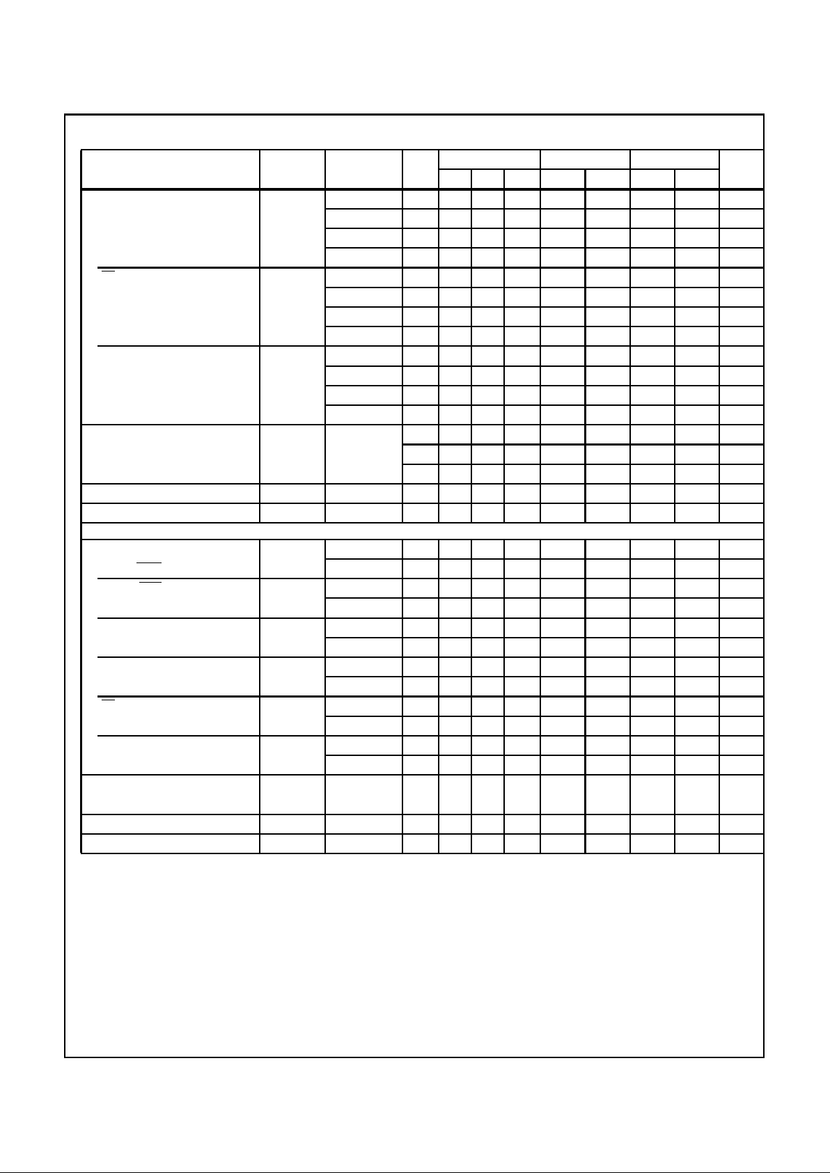
Prerequisite For Switching Specifications
PARAMETER SYMBOL
V
CC
(V)
25oC -40oC TO 85oC -55oC TO 125oC
UNITSMIN TYP MAX MIN MAX MIN MAX
HC TYPES
Pulse Width t
W
2 115 - - 145 - 175 - ns
CPU, CPD 4.5 23 - - 29 - 35 - ns
192 6 20 - - 25 - 30 - ns
t
W
2 100 - - 125 - 150 - ns
CPU, CPD 4.5 20 - - 25 - 30 - ns
193 6 17 - - 21 - 26 - ns
PL t
W
2 80 - - 100 - 120 - ns
4.5 16 - - 20 - 24 - ns
6 14 - - 17 - 20 - ns
MR t
W
2 100 - - 125 - 150 - ns
4.5 20 - - 25 - 30 - ns
6 17 - - 21 - 26 - ns
Set-up Time t
SU
2 80 - - 100 - 120 - ns
Pn to PL 4.5 16 - - 20 - 24 - ns
6 14 - - 17 - 20 - ns
Hold Time t
H
2 0--0-0-ns
Pn to PL 4.5 0 - - 0 - 0 - ns
6 0--0-0-ns
Hold Time t
H
2 80 - - 100 - 120 - ns
CPD to CPU or 4.5 16 - - 20 - 24 - ns
CPU to CPD 6 14 - - 17 - 20 - ns
Recovery Time t
REC
2 80 - - 100 - 120 - ns
PL to CPU, CPD 4.5 16 - - 20 - 24 - ns
6 14 - - 17 - 20 - ns
MR to CPU, CPD t
REC
2 5--5-5-ns
4.5 5--5-5-ns
6 5--5-5-ns
Maximum Frequency f
MAX
2 5--4-3-MHz
CPU, CPD 4.5 22 - - 18 - 15 - MHz
192 6 24 - - 21 - 18 - MHz
f
MAX
2 5--4-3-MHz
CPU, CPD 4.5 25 - - 20 - 17 - MHz
193 6 29 - - 24 - 20 - MHz
HCT TYPES
Pulse Width t
W
2 -------ns
CPU, CPD 4.5 23 - - 29 - 35 - ns
192 6 -------ns
CPU, CPD t
W
2 -------ns
193 4.5 23 - - 29 - 35 - ns
6 -------ns
CD74HC192, CD74HC193, CD74HCT193
6
PL t
W
2 -------ns
4.5 16 - - 20 - 24 - ns
6 -------ns
MR t
W
2 -------ns
4.5 20 - - 25 - 30 - ns
6 -------ns
Set-up Time t
SU
2 -------ns
Pn to PL 4.5 15 - - 19 - 22 - ns
6 -------ns
Hold Time t
H
2 -------ns
Pn to PL 4.5 0 - - 0 - 0 - ns
6 -------ns
Hold Time t
H
2 -------ns
CPD to CPU or 4.5 16 - - 20 - 24 - ns
CPU to CPD 6 - - - - - - - ns
Recovery Time t
REC
2 -------ns
PL to CPU, CPD 4.5 15 - - 19 - 22 - ns
6 -------ns
MR to CPU, CPD t
REC
2 -------ns
4.5 5--5-5-ns
6 -------ns
Maximum Frequency f
MAX
2 -------MHz
CPU, CPD 4.5 22 - - 18 - 15 - MHz
192 6 -------MHz
CPU, CPD f
MAX
2 -------MHz
193 4.5 22 - - 18 - 15 - MHz
6 -------MHz
Switching Specifications Input t
r
, tf = 6ns
PARAMETER SYMBOL
TEST
CONDITIONS
V
CC
(V)
25oC -40oC TO 85oC -55oC TO 125oC
UNITSMIN TYP MAX MIN MAX MIN MAX
HC TYPES
Propagation Delay t
PLH
, t
PHLCL
= 50pF 2 - - 125 - 155 - 190 ns
CPU to TCU CL= 50pF 4.5 - - 25 - 31 - 38 ns
CL= 15pF 5 - 10 - ----ns
CL= 50pF 6 - 21 - 26 - 32 ns
CPD to TCD t
PLH
, t
PHLCL
= 50pF 2 - - 125 - 155 - 190 ns
CL= 50pF 4.5 - - 25 - 31 - 38 ns
CL= 15pF 5 - 10 - ----ns
CL= 50pF 6 - - 21 - 26 - 32 ns
CPU to Q
n
t
PLH
, t
PHLCL
= 50pF 2 - - 220 - 270 - 325 ns
CL= 50pF 4.5 - - 43 - 54 - 65 ns
CL= 15pF 5 - 18 - ----ns
CL= 50pF 6 - - 37 - 46 - 55 ns
Prerequisite For Switching Specifications (Continued)
PARAMETER SYMBOL
V
CC
(V)
25oC -40oC TO 85oC -55oC TO 125oC
UNITSMIN TYP MAX MIN MAX MIN MAX
CD74HC192, CD74HC193, CD74HCT193
7
CPD to Q
n
t
PLH
, t
PHLCL
= 50pF 2 - - 220 - 270 - 325 ns
CL= 50pF 4.5 - - 43 - 54 - 65 ns
CL= 15pF 5 - 18 - - - - ns
CL= 50pF 6 - - 37 - 46 - 55 ns
PL to Q
n
t
PLH
, t
PHLCL
= 50pF 2 - - 220 - 275 - 330 ns
CL= 50pF 4.5 - - 44 - 55 - 66 ns
CL= 15pF 5 - 18 - ----ns
CL= 50pF 6 - - 37 - 47 - 56 ns
MR to Q
n
t
PHL
CL= 50pF 2 - - 200 - 250 - 300 ns
CL= 50pF 4.5 - - 40 - 50 - 60 ns
CL= 15pF 5 - 17 - ----ns
CL= 50pF 6 - - 34 - 43 - 51 ns
Transition Time t
TLH
, t
THLCL
= 50pF 2 - - 75 - 95 - 110 ns
Q, TCU, TCD 4.5 - - 15 - 19 - 22 ns
6 - - 13 - 16 - 19 ns
Input Capacitance C
IN
CL= 50pF - - - 10 - 10 - 10 pF
Power Dissipation Capacitance C
PD
CL= 15pF 5 - 40 - ----pF
HCT TYPES
Propagation Delay t
PLH
, t
PHLCL
= 50pF 4.5 - - 27 - 34 - 41 ns
CPU to TCU CL= 15pF 5 - 11 - ----ns
CPU to TCD t
PLH
, t
PHLCL
= 50pF 4.5 - - 27 - 34 - 41 ns
CL= 15pF 5 - 11 - ----ns
CPU to Q
n
t
PLH
, t
PHLCL
= 50pF 4.5 - - 40 - 50 - 60 ns
CL= 15pF 5 - 17 - ----ns
CPD to Q
n
t
PLH
, t
PHLCL
= 50pF 4.5 - - 40 - 50 - 60 ns
CL= 15pF 5 - 17 - ----ns
PL to Q
n
t
PLH
, t
PHLCL
= 50pF 4.5 - - 46 - 58 - 69 ns
CL= 15pF 5 - 21 - ----ns
MR to Q
n
t
PHL
CL= 50pF 4.5 - - 43 - 54 - 65 ns
CL= 15pF 5 - 18 - ----ns
Transition Time t
TLH
, t
THLCL
= 50pF
Q, TCU, TCD 4.5 - - 15 - 19 - 22 ns
Input Capacitance C
IN
CL= 50pF - - - 10 - 10 - 10 pF
Power Dissipation Capacitance C
PD
CL= 15pF 5 - 50 - ----pF
NOTES:
5. CPD is used to determine the dynamic power consumption, per gate.
6. PD = V
CC
2
fi + ∑ (CL V
CC
2
) where fi = Input Frequency, CL = Output Load Capacitance, VCC = Supply Voltage.
Switching Specifications Input t
r
, tf = 6ns (Continued)
PARAMETER SYMBOL
TEST
CONDITIONS
V
CC
(V)
25oC -40oC TO 85oC -55oC TO 125oC
UNITSMIN TYP MAX MIN MAX MIN MAX
CD74HC192, CD74HC193, CD74HCT193

8
Test Circuits and Waveforms
FIGURE 1. CD74HC192 SYNCHRONOUS DECADE COUNTERS, TYPICAL RESET, PRESET AND COUNT SEQUENCES
MASTER RESET
ASYNCHRONOUS PARALLEL LOAD
PRESET DATA
P0
P1
P2
P3
CLOCK UP
CLOCK DOWN
OUTPUTS
Q
0
Q
1
Q
2
Q
3
TERMINAL COUNT UP
TERMINAL COUNT DOWN
07
89012
COUNT DOWNCOUNT UPRESET
10987
PRESET
SEQUENCES:
1. RESET OUTPUTS TO ZERO.
2. LOAD (PRESET) TO BCD SEVEN.
TERMINAL COUNT UP, ZERO,
3. COUNT UP TO EIGHT, NINE,
ONE AND TWO.
4. COUNT DOWN TO ONE, ZERO,
TERMINAL COUNT DOWN, NINE,
EIGHT AND SEVEN.
CD74HC192, CD74HC193, CD74HCT193

9
FIGURE 2. CD74HC193 SYNCHRONOUS BINARY COUNTERS, TYPICAL RESET, PRESET AND COUNT SEQUENCES
FIGURE 3. CLOCK TO OUTPUT DELAYSAND CLOCK PULSE
WIDTH
FIGURE 4. CLOCK TO TERMINAL COUNT DELAYS
FIGURE 5. PARALLEL LOAD PULSE WIDTH, PARALLEL
LOAD TO OUTPUT DELAYS, AND PARALLEL
LOAD TO CLOCK RECOVERY TIME
FIGURE 6. MASTER RESET PULSE WIDTH, MASTER RESET
TO OUTPUT DELAY AND MASTER RESET TO
CLOCK RECOVERY TIME
Test Circuits and Waveforms
(Continued)
MASTER RESET
ASYNCHRONOUS PARALLEL LOAD
PRESET DATA
P0
P1
P2
P3
CLOCK UP
CLOCK DOWN
OUTPUTS
Q
0
Q
1
Q
2
Q
3
TERMINAL COUNT UP
TERMINAL COUNT DOWN
013
14 15 0 1 2
COUNT DOWNCOUNT UPRESET
1 0 15 14 13
PRESET
SEQUENCES:
1. RESET OUTPUTS TO ZERO.
2. LOAD (PRESET) TO BINARY THIRTEEN.
3. COUNT UP TO FOURTEEN,
FIFTEEN, TERMINAL COUNT UP,
ZERO, ONE AND TWO.
4. COUNT DOWN TO ONE, ZERO,
TERMINAL COUNT DOWN,
FIFTEEN, FOURTEEN AND
THIRTEEN.
NOTES:
1. Master reset overrides load data and clock inputs.
2. When counting up, clock-down input must be high.
When counting down, clock-up input must be high.
CPU OR CPD
l/f
MAX
INPUT LEVEL
V
S
V
S
V
S
t
PHL
t
PLH
V
S
Q
n
V
S
t
W
INPUT LEVEL
TCU OR TCD
t
PHL
t
PLH
V
S
V
S
CPU OR CPD
V
S
V
S
INPUT LEVEL
INPUT LEVEL
INPUT LEVEL
CPU OR CPD
V
S
V
S
t
PLH
Q
n
V
S
t
W
V
S
V
S
V
S
t
W
Pn
PL
t
PHL
t
REC
V
S
MR
CPU OR CPD
Q
n
t
PHL
V
S
V
S
INPUT LEVEL
t
REC
INPUT LEVEL
V
S
V
S
t
W
CD74HC192, CD74HC193, CD74HCT193

10
FIGURE 7. SET-UP AND HOLD TIMES DATA TO PARALLEL LOAD (PL)
FIGURE 8. CASCADED UP/DOWN COUNTER WITH PARALLEL LOAD
NOTE: Illegal states in BCD counters corrected in one count. NOTE: Illegal states in BCD counters corrected in one or two counts.
FIGURE 9. CD74HC192, CD74HCT193 STATE DIAGRAMS
Test Circuits and Waveforms
(Continued)
INPUT LEVEL
INPUT LEVEL
Q = p
V
S
t
H
tSU(L)
Q = p
Q
n
PL
Pn
t
SU
(H)
V
S
V
S
t
H
P0 P1 P2 P3
TCU
TCD
MR
Q
0Q1Q2Q3
CPU
CPD
PL
UP CLOCK
DOWN CLOCK
ASYNCHRONOUS,
PARALLEL LOAD
RESET
OUTPUT
CARRY
BORROW
DATA INPUT
P0 P1 P2 P3
TCU
TCD
MR
Q
0Q1Q2Q3
CPU
CPD
PL
234
5
6
7
89101112
13
14
15
10
COUNT UP
234
5
6
7
89101112
13
14
15
10
COUNT DOWN
CD74HC192, CD74HC193, CD74HCT193

IMPORTANT NOTICE
T exas Instruments and its subsidiaries (TI) reserve the right to make changes to their products or to discontinue
any product or service without notice, and advise customers to obtain the latest version of relevant information
to verify, before placing orders, that information being relied on is current and complete. All products are sold
subject to the terms and conditions of sale supplied at the time of order acknowledgement, including those
pertaining to warranty, patent infringement, and limitation of liability.
TI warrants performance of its semiconductor products to the specifications applicable at the time of sale in
accordance with TI’s standard warranty. Testing and other quality control techniques are utilized to the extent
TI deems necessary to support this warranty. Specific testing of all parameters of each device is not necessarily
performed, except those mandated by government requirements.
CERT AIN APPLICATIONS USING SEMICONDUCTOR PRODUCTS MAY INVOLVE POTENTIAL RISKS OF
DEATH, PERSONAL INJURY, OR SEVERE PROPERTY OR ENVIRONMENTAL DAMAGE (“CRITICAL
APPLICATIONS”). TI SEMICONDUCTOR PRODUCTS ARE NOT DESIGNED, AUTHORIZED, OR
WARRANTED TO BE SUITABLE FOR USE IN LIFE-SUPPORT DEVICES OR SYSTEMS OR OTHER
CRITICAL APPLICATIONS. INCLUSION OF TI PRODUCTS IN SUCH APPLICA TIONS IS UNDERSTOOD T O
BE FULLY AT THE CUSTOMER’S RISK.
In order to minimize risks associated with the customer’s applications, adequate design and operating
safeguards must be provided by the customer to minimize inherent or procedural hazards.
TI assumes no liability for applications assistance or customer product design. TI does not warrant or represent
that any license, either express or implied, is granted under any patent right, copyright, mask work right, or other
intellectual property right of TI covering or relating to any combination, machine, or process in which such
semiconductor products or services might be or are used. TI’s publication of information regarding any third
party’s products or services does not constitute TI’s approval, warranty or endorsement thereof.
Copyright 1998, Texas Instruments Incorporated
 Loading...