

Datasheet CD74HCT163E, CD74HCT161M96, CD74HCT161M, CD74HCT161E, CD74HCT163M96 Datasheet (Texas Instruments)
...
CD74HC161, CD74HCT161,
/
j
/
/
[ /Title
(CD74
HC161
,
CD74
HCT16
1,
CD74
HC163
,
CD74
HCT16
3)
Subect
(High
Speed
CMOS
Logic
Presettable
Counte
rs)
Autho
r ()
Key-
words
(High
Speed
CMOS
Logic
Presettable
Counte
rs,
High
Speed
Data sheet acquired from Harris Semiconductor
SCHS154
February 1998
Features
• CD74HC161, CD74HCT161 4-Bit Binary Counter,
Asynchronous Reset
• CD74HC163, CD74HCT163 4-Bit Binary Counter,
Synchronous Reset
• Synchronous Counting and Loading
• Two Count Enable Inputs for n-Bit Cascading
• Look-Ahead Carry for High-Speed Counting
• Fanout (Over Temperature Range)
- Standard Outputs. . . . . . . . . . . . . . . 10 LSTTL Loads
- Bus Driver Outputs . . . . . . . . . . . . . 15 LSTTL Loads
o
• Wide Operating Temperature Range . . . -55
• Balanced Propagation Delay and Transition Times
• Significant Power Reduction Compared to LSTTL
Logic ICs
• HC Types
- 2V to 6V Operation
- High Noise Immunity: N
at VCC = 5V
• HCT Types
- 4.5V to 5.5V Operation
- Direct LSTTL Input Logic Compatibility,
V
= 0.8V (Max), VIH = 2V (Min)
IL
- CMOS Input Compatibility, I
= 30%, NIH = 30% of V
IL
≤ 1µA at VOL, V
l
C to 125oC
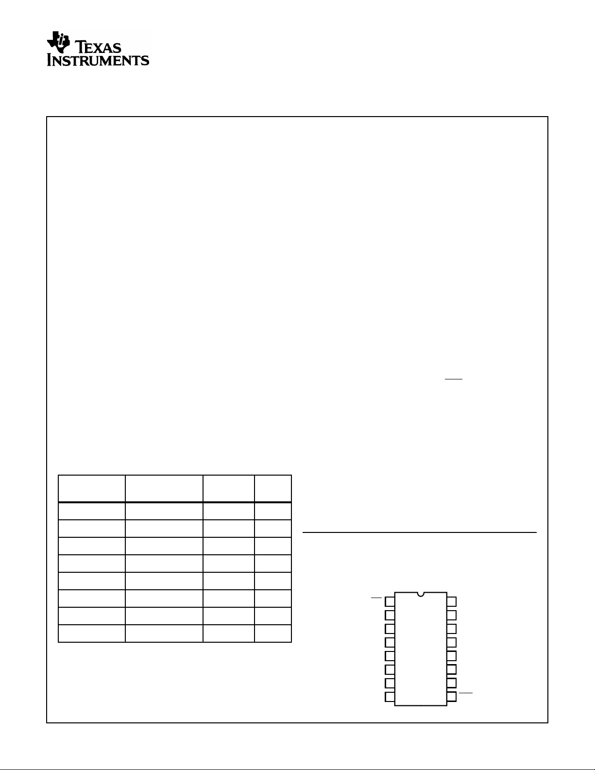
Ordering Information
PART NUMBER TEMP. RANGE (oC) PACKAGE
CD74HC161E -55 to 125 16 Ld PDIP E16.3
CD74HC161M -55 to 125 16 Ld SOIC M16.15
CD74HC163E -55 to 125 16 Ld PDIP E16.3
CD74HC163M -55 to 125 16 Ld SOIC M16.15
CD74HCT161E -55 to 125 16 Ld PDIP E16.3
CD74HCT161M -55 to 125 16 Ld SOIC M16.15
CD74HCT163E -55 to 125 16 Ld PDIP E16.3
CD74HCT163M -55 to 125 16 Ld SOIC M16.15
NOTES:
1. When ordering,usetheentire partnumber.Addthesuffix 96 toobtain the variant in the tape and reel.
2. Waferand die for this part number is availablewhich meets allelectrical specifications. Please contact your local sales office or Harris
customer service for ordering information.
CD74HC163, CD74HCT163
High Speed CMOS Logic
Presettable Counters
Description
The Harris CD74HC161, CD74HCT161, CD74HC163 and
CD74HCT163 are presettable synchronous counters that
feature look-ahead carry logic for use in high-speed
counting applications. The CD74HC161 and CD74HCT161
are asynchronous reset decade and binary counters,
respectively; the CD74HC163 and CD74HCT163 devices
decade and binary counters, respectively and are reset
synchronously with the clock. Counting and parallel
presetting are both accomplished synchronously with the
negative-to-positive transition of the clock.
A low level on the synchronous parallel enable input, SPE,
disables countingoperation and allows data at the P0 to P3
inputs to be loaded into the counter (provided that the
setup and hold requirements for SPE are met).
All counters are reset with a low level on the Master Reset
input, MR. In the CD74HC163 and CD74HCT163 counters
(synchronous reset types), the requirements for setup and
hold time with respect to the clock must be met.
Two count enables, PE and TE, in each counter are
CC
provided for n-bit cascading. In all counters reset action
OH
PKG.
NO.
occurs regardless of the level of the
(and the clock input, CP, in the CD74HC161 and
CD74HCT161 types).
If a decade counter is preset to an illegal state or assumes
an illegal state when power is applied, it will return to the
normal sequence in one count as shown in state diagram.
The look-ahead carry feature simplifies ser ial cascading of
the counters. Both count enable inputs (PE and TE) must
be high to count. The TE input is gated with the Q outputs
of all four stages so that at the maximum count the terminal
count (TC) output goes high for one clock period. This TC
pulse is used to enable the next cascaded stage.
Pinout
CD74HC161, CD74HCT161, CD74HC163, CD74HCT163
(PDIP, SOIC)
TOP VIEW
1
MR
2
CP
3
P0
4
P1
5
P2
6
P3
7
PE
8
GND
SPE, PE and TE inputs
16
V
CC
TC
15
14
Q0
13
Q1
12
Q2
Q3
11
10
TE
9
SPE
CAUTION: These devices are sensitive to electrostatic discharge. Users should follow proper IC Handling Procedures.
Copyright
© Harris Corporation 1998
1
File Number 1550.1
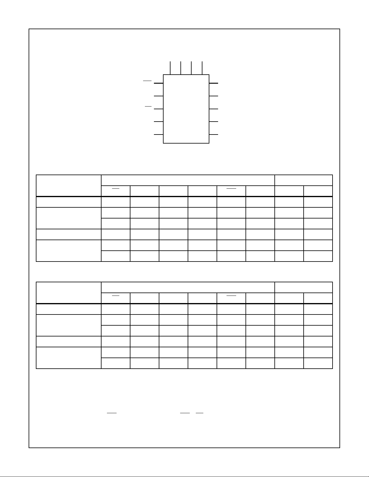
CD74HC161, CD74HCT161, CD74HC163, CD74HCT163
Functional Diagram
P0 P1 P2 P3
3456
SPE
CP
MR
PE
TE
9
2
1
7
10
14
Q0
13
Q1
12
Q2
11
Q3
15
TC
MODE SELECT - FUNCTION TABLE FOR CD74HC/HCT161
INPUTS OUTPUTS
OPERATING MODE
MR CP PE TE SPE P
n
Q
n
TC
Reset (Clear) L XXXXXLL
Parallel Load H ↑ XXl l LL
H ↑ X X l h H (Note 3)
Count H ↑ h h h (Note 5) X Count (Note 3)
Inhibit H X I (Note 4) X h (Note 5) X q
H X X I (Note 4) h (Note 5) X q
n
n
(Note 3)
L
MODE SELECT - FUNCTION TABLE FOR CD74HC/HCT163
INPUTS OUTPUTS
OPERATING MODE
MR CP PE TE SPE P
n
Q
n
TC
Reset (Clear) l ↑ XXXXLL
Parallel Load h (Note 5) ↑ XX l l LL
h (Note 5) ↑ X X l h H (Note 3)
Count h (Note 5) ↑ h h h (Note 5) X Count (Note 3)
Inhibit h (Note 5) X I (Note 4) X h (Note 5) X q
h (Note 5) X X I (Note 4) h (Note 5) X q
n
n
(Note 3)
L
NOTE: H = High voltage level steady state; L = Low voltagelevel steady state; h = High voltage level one setup time prior to the Low-to-High
clock transition; l = Low voltage level one setup time prior to the Low-to-High clock transition; X = Don’t Care; q = Lower case letters indicate
the state of the referenced output prior to the Low-to-High clock transition; ↑ = Low-to-High clock transition.
3. The TC output is High when TE is High and the counter is at Terminal Count (HHHH for CD74HC/HCT161 and CD74HC/HCT163).
4. The High-to-Low transition of PE or TE on the CD74HC/HCT161 and the CD74HC/HCT163 should only occur while CP is HIGH for conventional operation.
5. The Low-to-Hightransition of SPEon the CD74HC/HCT161and SPEor MR onthe CD74HC/HCT163 should only occurwhile CP isHIGH
for conventional operation.
2
CD74HC161, CD74HCT161, CD74HC163, CD74HCT163
Absolute Maximum Ratings Thermal Information
DC Supply Voltage, VCC. . . . . . . . . . . . . . . . . . . . . . . . -0.5V to 7V
DC Input Diode Current, I
IK
For VI < -0.5V or VI > VCC + 0.5V. . . . . . . . . . . . . . . . . . . . . .±20mA
DC Output Diode Current, I
OK
For VO < -0.5V or VO > VCC + 0.5V . . . . . . . . . . . . . . . . . . . .±20mA
DC Drain Current, per Output, I
O
For -0.5V < VO < VCC + 0.5V. . . . . . . . . . . . . . . . . . . . . . . . . .±25mA
DC Output Source or Sink Current per Output Pin, I
O
For VO > -0.5V or VO < VCC + 0.5V . . . . . . . . . . . . . . . . . . . .±25mA
DC VCC or Ground Current, ICC . . . . . . . . . . . . . . . . . . . . . . . . .±50mA
Operating Conditions
Temperature Range, TA . . . . . . . . . . . . . . . . . . . . . . -55oC to 125oC
Supply Voltage Range, V
HC Types . . . . . . . . . . . . . . . . . . . . . . . . . . . . . . . . . . . . .2V to 6V
HCT Types . . . . . . . . . . . . . . . . . . . . . . . . . . . . . . . . .4.5V to 5.5V
DC Input or Output Voltage, VI, VO . . . . . . . . . . . . . . . . . 0V to V
Input Rise and Fall Time
2V . . . . . . . . . . . . . . . . . . . . . . . . . . . . . . . . . . . . . . 1000ns (Max)
4.5V. . . . . . . . . . . . . . . . . . . . . . . . . . . . . . . . . . . . . . 500ns (Max)
6V . . . . . . . . . . . . . . . . . . . . . . . . . . . . . . . . . . . . . . . 400ns (Max)
CAUTION: Stresses above those listed in “Absolute Maximum Ratings” may cause permanent damage to the device. This is a stress only rating and operation
of the device at these or any other conditions above those indicated in the operational sections of this specification is not implied.
NOTE:
6. θJA is measured with the component mounted on an evaluation PC board in free air.
CC
Thermal Resistance (Typical, Note 6) θJA (oC/W)
PDIP Package. . . . . . . . . . . . . . . . . . . . . . . . . . . . . 90
SOIC Package. . . . . . . . . . . . . . . . . . . . . . . . . . . . . 160
Maximum Junction Temperature . . . . . . . . . . . . . . . . . . . . . . . 150oC
Maximum Storage Temperature Range . . . . . . . . . .-65oC to 150oC
Maximum Lead Temperature (Soldering 10s) . . . . . . . . . . . . .300oC
(SOIC - Lead Tips Only)
CC
DC Electrical Specifications
PARAMETER SYMBOL
HC TYPES
High Level Input
Voltage
Low Level Input
Voltage
High Level Output
Voltage
CMOS Loads
High Level Output
Voltage
TTL Loads
Low Level Output
Voltage
CMOS Loads
Low Level Output
Voltage
TTL Loads
Input Leakage
Current
V
IH
V
IL
V
OH
V
OL
I
I
TEST
CONDITIONS
(V) IO(mA) MIN TYP MAX MIN MAX MIN MAX
I
V
CC
(V)
o
C -40oC TO 85oC -55oC TO 125oC
25
UNITSV
- - 2 1.5 - - 1.5 - 1.5 - V
4.5 3.15 - - 3.15 - 3.15 - V
6 4.2 - - 4.2 - 4.2 - V
- - 2 - - 0.5 - 0.5 - 0.5 V
4.5 - - 1.35 - 1.35 - 1.35 V
6 - - 1.8 - 1.8 - 1.8 V
VIHor VIL-0.02 2 1.9 - - 1.9 - 1.9 - V
-0.02 4.5 4.4 - - 4.4 - 4.4 - V
-0.02 6 5.9 - - 5.9 - 5.9 - V
- - ---- - - - V
-4 4.5 3.98 - - 3.84 - 3.7 - V
-5.2 6 5.48 - - 5.34 - 5.2 - V
VIHor VIL0.02 2 - - 0.1 - 0.1 - 0.1 V
0.02 4.5 - - 0.1 - 0.1 - 0.1 V
0.02 6 - - 0.1 - 0.1 - 0.1 V
- - ---- - - - V
4 4.5 - - 0.26 - 0.33 - 0.4 V
5.2 6 - - 0.26 - 0.33 - 0.4 V
VCC or
-6--±0.1 - ±1-±1 µA
GND
3

CD74HC161, CD74HCT161, CD74HC163, CD74HCT163
DC Electrical Specifications (Continued)
TEST
CONDITIONS
PARAMETER SYMBOL
Quiescent Device
I
CC
Current
HCT TYPES
High Level Input
V
IH
Voltage
Low Level Input
Voltage
High Level Output
V
IL
V
OH
Voltage
CMOS Loads
High Level Output
Voltage
TTL Loads
Low Level Output
V
OL
Voltage
CMOS Loads
Low Level Output
Voltage
TTL Loads
Input Leakage
Current
Quiescent Device
I
I
I
CC
Current
Additional Quiescent
Device Current Per
∆I
CC
(Note)
Input Pin: 1 Unit Load
NOTE: For dual-supply systems theoretical worst case (V
(V) IO(mA) MIN TYP MAX MIN MAX MIN MAX
I
VCC or
0 6 - - 8 - 80 - 160 µA
GND
- - 4.5 to
- - 4.5 to
VIHor VIL-0.02 4.5 4.4 - - 4.4 - 4.4 - V
-4 4.5 3.98 - - 3.84 - 3.7 - V
VIHor VIL0.02 4.5 - - 0.1 - 0.1 - 0.1 V
4 4.5 - - 0.26 - 0.33 - 0.4 V
VCCand
0 5.5 - ±0.1 - ±1-±1 µA
GND
VCC or
0 5.5 - - 8 - 80 - 160 µA
GND
V
CC
- 4.5 to
-2.1
o
C -40oC TO 85oC -55oC TO 125oC
V
CC
25
(V)
2--2- 2 - V
5.5
- - 0.8 - 0.8 - 0.8 V
5.5
- 100 360 - 450 - 490 µA
5.5
= 2.4V, VCC = 5.5V) specification is 1.8mA.
I
UNITSV
HCT Input Loading Table
INPUT UNIT LOADS
P0 - P3 0.25
PE 0.65
CP 1.05
MR 0.8
SPE 0.5
TE 1.05
NOTE: Unit Load is ∆ICClimit specified in DC Electrical Table,e.g.,
360µA max at 25oC.
Prerequisite For Switching Specifications
PARAMETER SYMBOL
HC TYPES
Maximum CP Frequency
(Note7)
f
MAX
TEST
CONDITIONS
- 2 6 - - 5 - 4 - MHz
V
CC
(V)
25oC -40oC TO 85oC -55oC TO 125oC
UNITSMIN TYP MAX MIN MAX MIN MAX
4.5 30 - - 24 - 20 - MHz
6 35 - - 28 - 24 - MHz
4

CD74HC161, CD74HCT161, CD74HC163, CD74HCT163
Prerequisite For Switching Specifications (Continued)
PARAMETER SYMBOL
CP Width (Low) t
MR Pulse Width (161) t
Setup Time, Pn to CP t
Setup Time, PE or TE to CP t
Setup Time, SPE to CP t
Setup Time, MR to CP (163) t
Hold Time, PN to CP t
Hold Time, TE or PE to CP t
Hold Time, SPE to CP t
Recovery Time, MR to CP (161) t
HCT TYPES
Maximum CP Frequency f
CP Width (Low) (Note 7) t
MR Pulse Width (161) t
Setup Time, Pn to CP t
Setup Time, PE or TE to CP t
Setup Time, SPE to CP t
Setup Time, MR to CP (163) t
Hold Time, PN to CP t
Hold Time, TE or PE to CP t
W(L)
W
SU
SU
SU
SU
H
H
H
REC
MAX
W(L)
W
SU
SU
SU
SU
H
H
TEST
CONDITIONS
V
CC
(V)
25oC -40oC TO 85oC -55oC TO 125oC
- 2 80 - - 100 - 120 - ns
4.5 16 - - 20 - 24 - ns
6 14 - - 17 - 20 - ns
- 2 100 - - 125 - 150 - ns
4.5 20 - - 25 - 30 - ns
6 17 - - 21 - 26 - ns
- 2 60 - - 75 - 90 - ns
4.5 12 - - 15 - 18 - ns
6 10 - - 13 - 15 - ns
- 2 50 - - 65 - 75 - ns
4.5 10 - - 13 - 15 - ns
6 9 - - 11 - 13 - ns
- 2 60 - - 75 - 90 - ns
4.5 12 - - 15 - 18 - ns
6 10 - - 13 - 15 - ns
- 2 65 - - 80 - 100 - ns
4.5 13 - - 16 - 20 - ns
6 11 - - 14 - 17 - ns
-23--3-3-ns
4.5 3 - - 3 - 3 - ns
63--3-3-ns
-20--0-0-ns
4.5 0 - - 0 - 0 - ns
60--0-0-ns
-20--0-0-ns
4.5 0 - - 0 - 0 - ns
60--0-0-ns
- 2 75 - - 95 - 110 - ns
4.5 15 - - 19 - 22 - ns
6 13 - - 16 - 19 - ns
- 4.5 30 - - 24 - 20 - MHz
- 4.5 16 - - 20 - 24 - ns
- 4.5 20 - - 25 - 30 - ns
- 4.5 10 - - 13 - 15 - ns
- 4.5 13 - - 16 - 20 - ns
- 4.5 12 - - 15 - 18 - ns
- 4.5 13 - - 16 - 20 - ns
- 4.5 5 - - 5 - 5 - ns
- 4.5 3 - - 3 - 3 - ns
UNITSMIN TYP MAX MIN MAX MIN MAX
5

CD74HC161, CD74HCT161, CD74HC163, CD74HCT163
Prerequisite For Switching Specifications (Continued)
25oC -40oC TO 85oC -55oC TO 125oC
UNITSMIN TYP MAX MIN MAX MIN MAX
PARAMETER SYMBOL
Hold Time, SPE to CP t
Recovery Time, MR to CP (161) t
H
REC
TEST
CONDITIONS
V
CC
(V)
- 4.5 3 - - 3 - 3 - ns
- 4.5 15 - - 19 - 22 - ns
NOTE:
7. Applies to non-cascaded operation only. With cascaded counters clock to terminal count propagation delays, count enables (PE or TE)to-clock setup times, and count enables (PE or TE)-to-clock hold times determine maximum clock frequency. For example with these HC
devices:
f
(CP)
MAX
----------------------------------------------------------------------------------------------------------------------------------------------------CP-to-TC prop. delay TE-to-CP setup TE-to-CP Hold++
Switching Specifications C
PARAMETER SYMBOL
1
= 50pF, Input tr, tf= 6ns
L
TEST
CONDITIONS V
CC
(V)
1
---------------------------- 37 10 0++
25oC
21MHz min()≈==
-40oC TO
85oC
-55oC TO
125oC
UNITSMIN TYP MAX MIN MAX MIN MAX
HC TYPES
Propagation Delay t
PHL
, t
PLHCL
= 50pF
CP to TC 2 - - 185 - 230 - 280 ns
4.5 - - 37 - 46 - 56 ns
CL = 15pF 5 - 15 - - - - - ns
CL = 50pF 6 - - 31 - 39 - 48 ns
CP to Qn t
TE to TC t
MR to Qn (161) t
MR to TC (161) t
Output Transition Time t
PHL, tPLH
PHL, tPLH
PHL
PHL
, t
THL
TLH
CL = 50pF 2 - - 185 - 230 - 280 ns
4.5 - - 37 - 46 - 56 ns
CL = 15pF 5 - 15 - - - - - ns
CL = 50pF 6 - - 31 - 39 - 48 ns
CL = 50pF 2 - - 120 - 150 - 180 ns
4.5 - - 24 - 30 - 36 ns
CL = 15pF 5 - 9 - - - - - ns
CL = 50pF 6 - - 20 - 26 - 31 ns
CL = 50pF 2 - - 210 - 265 - 315 ns
4.5 - - 42 - 53 - 63 ns
CL = 15pF 5 - 18 - - - - - ns
CL = 50pF 6 - - 36 - 45 - 54 ns
CL = 50pF 2 - - 210 - 265 - 315 ns
4.5 - - 42 - 53 - 63 ns
CL = 50pF 6 - - 36 - 45 - 54 ns
CL = 50pF 2 - - 75 - 95 - 110 ns
4.5 - - 15 - 19 - 22 ns
Power Dissipation Capacitance
(Notes 8, 9)
6 - - 13 - 16 - 19 ns
C
PD
-5-60-----pF
6

CD74HC161, CD74HCT161, CD74HC163, CD74HCT163
Switching Specifications C
PARAMETER SYMBOL
Input Capacitance C
HCT TYPES
Propagation Delay
CP to TC t
CP to Qn t
TE to TC t
MR to Qn (161) t
MR to TC (161) t
Output Transition Time t
Power Dissipation Capacitance
(Notes 6, 7)
PHL, tPLH
PHL, tPLH
PHL, tPLH
THL
= 50pF, Input tr, tf= 6ns (Continued)
L
TEST
CONDITIONS VCC(V)
IN
CL = 50pF - 10 - 10 - 10 - 10 pF
CL = 50pF 4.5 - - 42 - 53 - 63 ns
CL = 15pF 5 - 18 - - - - - ns
CL = 50pF 4.5 - - 39 - 49 - 59 ns
CL = 15pF 5 - 16 - - - - - ns
CL = 50pF 4.5 - - 32 - 40 - 48 ns
CL = 15pF 5 - 13 - - - - - ns
PHL
CL = 50pF 4.5 - - 50 - 63 - 75 ns
CL = 15pF 5 - 21 - - - - - ns
PHL
C
, t
PD
CL = 50pF 4.5 - - 50 - 63 - 75 ns
CL = 50pF 4.5 - - 15 - 19 - 22 ns
TLH
-5-63-----pF
25oC
-40oC TO
85oC
-55oC TO
125oC
UNITSMIN TYP MAX MIN MAX MIN MAX
Input Capacitance C
IN
CL = 50pF - 10 - 10 - 10 - 10 pF
NOTES:
8. CPD is used to determine the dynamic power consumption, per package.
9. PD=CPDV
CC
2
fi+ ∑(CLV
2
fO) where fi= Input Frequency, fO= Output Frequency, CL= Output Load Capacitance, VCC= Supply
CC
Voltage.
7

Timing Diagram
CD74HC161, CD74HCT161, CD74HC163, CD74HCT163
MASTER RESET (161)
MASTER RESET (163)
SPE
P0
PRESET
DAT A
INPUTS
COUNT
ENABLES
OUTPUTS
P1
P2
P3
CP (161)
CP (163)
PE
TE
Q0
Q1
Q2
(ASYNCHRONOUS)
(SYNCHRONOUS)
Q3
TC
12 13 14 15 0 1 2
RESET PRESET
Sequence illustrated on waveforms:
1. Reset outputs to zero.
2. Preset to binary twelve.
3. Count to thirteen, fourteen, fifteen, zero, one, and two.
4. Inhibit.
COUNT INHIBIT
8

CD74HC161, CD74HCT161, CD74HC163, CD74HCT163
Test Circuits and Waveforms
trC
L
CLOCK
10%
90%
50%
10%
tfC
t
L
WL
tWL+ tWH=
50%
t
WH
fC
50%
1.3V
I
fC
L
3V
GND
+ tWH=
t
t
WL
WH
I
L
V
CC
GND
trCL= 6ns
CLOCK
0.3V
2.7V
1.3V
0.3V
t
fCL
t
WL
= 6ns
1.3V
NOTE: Outputs should be switching from 10% VCC to 90% VCC in
accordance with device truth table.For f
, input duty cycle = 50%.
MAX
FIGURE 1. HC CLOCK PULSE RISE AND FALL TIMES AND
PULSE WIDTH
tr = 6ns tf = 6ns
V
t
CC
GND
TLH
INPUT
t
90%
50%
10%
THL
90%
t
PLH
50%
10%
INVERTING
OUTPUT
t
PHL
FIGURE 3. HC TRANSITION TIMES AND PROPAGATION
DELAY TIMES, COMBINATION LOGIC
tfC
L
V
CC
50%
GND
t
H(L)
V
CC
50%
t
SU(L)
GND
CLOCK
INPUT
DAT A
INPUT
t
SU(H)
trC
L
90%
10%
t
H(H)
NOTE: Outputs should be switching from 10% VCC to 90% VCC in
accordance with device truth table.For f
, input duty cycle = 50%.
MAX
FIGURE 2. HCT CLOCK PULSE RISE AND FALL TIMES AND
PULSE WIDTH
= 6ns
tr = 6ns
INPUT
t
2.7V
1.3V
0.3V
THL
t
f
3V
GND
t
TLH
90%
t
PLH
1.3V
10%
INVERTING
OUTPUT
t
PHL
FIGURE 4. HCT TRANSITION TIMES AND PROPAGATION
DELAY TIMES, COMBINATION LOGIC
CLOCK
INPUT
DAT A
INPUT
t
SU(H)
trC
L
2.7V
0.3V
t
H(H)
1.3V
1.3V
tfC
L
3V
1.3V
GND
t
H(L)
3V
1.3V
t
SU(L)
GND
OUTPUT
t
REM
V
CC
SET, RESET
OR PRESET
50%
90%
t
PLH
IC
t
TLH
t
THL
90%
50%
10%
t
PHL
GND
C
L
50pF
FIGURE 5. HC SETUP TIMES, HOLD TIMES, REMOVAL TIME,
AND PROPAGATION DELAY TIMES FOR EDGE
TRIGGERED SEQUENTIAL LOGIC CIRCUITS
OUTPUT
t
REM
3V
SET, RESET
1.3V
90%
1.3V
t
t
PLH
TLH
90%
1.3V
10%
t
PHL
t
THL
OR PRESET
IC
C
L
50pF
FIGURE 6. HCT SETUP TIMES, HOLD TIMES, REMOVALTIME,
AND PROPAGATION DELAY TIMES FOR EDGE
TRIGGERED SEQUENTIAL LOGIC CIRCUITS
9
GND

IMPORTANT NOTICE
T exas Instruments and its subsidiaries (TI) reserve the right to make changes to their products or to discontinue
any product or service without notice, and advise customers to obtain the latest version of relevant information
to verify, before placing orders, that information being relied on is current and complete. All products are sold
subject to the terms and conditions of sale supplied at the time of order acknowledgement, including those
pertaining to warranty, patent infringement, and limitation of liability.
TI warrants performance of its semiconductor products to the specifications applicable at the time of sale in
accordance with TI’s standard warranty. Testing and other quality control techniques are utilized to the extent
TI deems necessary to support this warranty . Specific testing of all parameters of each device is not necessarily
performed, except those mandated by government requirements.
CERTAIN APPLICATIONS USING SEMICONDUCTOR PRODUCTS MAY INVOLVE POTENTIAL RISKS OF
DEATH, PERSONAL INJURY, OR SEVERE PROPERTY OR ENVIRONMENTAL DAMAGE (“CRITICAL
APPLICATIONS”). TI SEMICONDUCTOR PRODUCTS ARE NOT DESIGNED, AUTHORIZED, OR
WARRANTED TO BE SUITABLE FOR USE IN LIFE-SUPPORT DEVICES OR SYSTEMS OR OTHER
CRITICAL APPLICA TIONS. INCLUSION OF TI PRODUCTS IN SUCH APPLICATIONS IS UNDERST OOD TO
BE FULLY AT THE CUSTOMER’S RISK.
In order to minimize risks associated with the customer’s applications, adequate design and operating
safeguards must be provided by the customer to minimize inherent or procedural hazards.
TI assumes no liability for applications assistance or customer product design. TI does not warrant or represent
that any license, either express or implied, is granted under any patent right, copyright, mask work right, or other
intellectual property right of TI covering or relating to any combination, machine, or process in which such
semiconductor products or services might be or are used. TI’s publication of information regarding any third
party’s products or services does not constitute TI’s approval, warranty or endorsement thereof.
Copyright 1998, Texas Instruments Incorporated
 Loading...