

1
Data sheet acquired from Harris Semiconductor
SCHS254
Features
• Buffered Inputs
• Typical Propagation Delay: 5.3ns at V
CC
= 5V,
T
A
= 25oC, CL = 50pF
• SCR Latchup Resistant BiCMOS Process and
Circuit Design
• Speed of Bipolar FAST™/AS/S
• 48mA Output Sink Current
• Output Voltage Swing Limited to 3.7V at V
CC
= 5V
• Controlled Output Edge Rates
• Input/Output Isolation to V
CC
• BiCMOS Technology with Low Quiescent Power
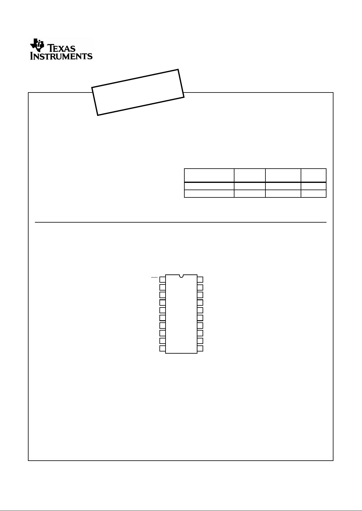
Pinout
Ordering Information
PART NUMBER
TEMP.
RANGE (oC) PACKAGE
PKG.
NO.
CD74FCT273E 0 to 70 20 Ld PDIP E20.3
CD74FCT273M 0 to 70 20 Ld SOIC M20.3
NOTE: When ordering the suffix M package, use the entire part
number. Add the suffix96 to obtainthe variant in the tape and reel.
CD74FCT273
(PDIP, SOIC)
TOP VIEW
11
12
13
14
15
16
17
18
20
19
10
9
8
7
6
5
4
3
2
1
MR
Q0
D0
D1
Q1
Q2
D3
D2
Q3
GND
V
CC
D7
D6
Q6
Q5
D5
D4
Q4
CP
Q7
January 1997
CAUTION: These devices are sensitive to electrostatic discharge. Users should follow proper IC Handling Procedures.
FAST™ is a trademark of Fairchild Semiconductor.
Copyright
© Harris Corporation 1997
CD74FCT273
BiCMOS FCT Interface Logic,
Octal D Flip-Flop with Reset
NO
T RECOMMENDED
FOR NEW DESIGNS
Use CMOS T
echnology
File Number 2303.2
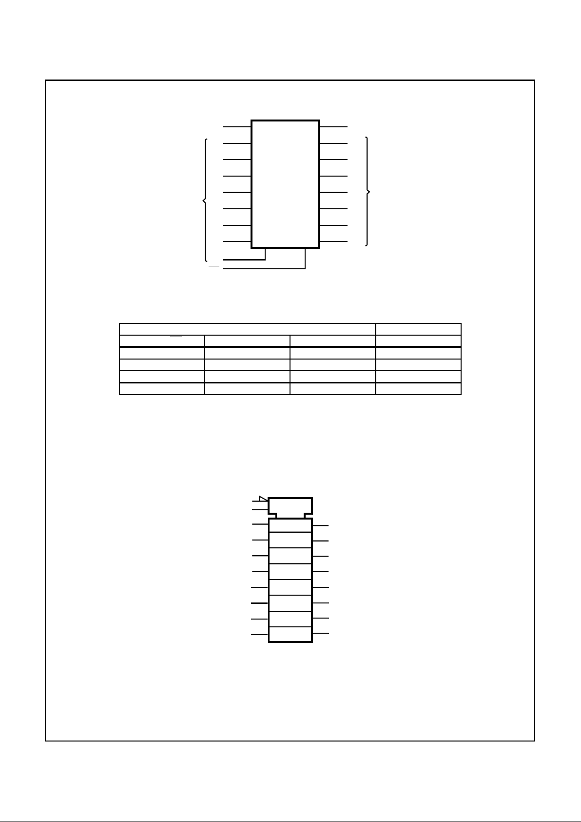
2
Functional Diagram
IEC Logic Symbol
TRUTH TABLE (Note 1)
INPUTS OUTPUTS
RESET MR CLOCK CP DATA Dn Qn
LXXL
H ↑ HH
H ↑ LL
HLXQ0
NOTE:
1. H = HIGH Voltage Level (Steady State)
L = LOW Voltage Level (Steady State)
X = Irrelevant
↑ = Transition from low to high level.
Q0 = The level of Q before the indicated steady state input conditions were established.
11
3
4
7
8
13
14
17
2
5
6
9
12
15
16
18
GND = PIN 10
V
CC
= PIN 20
1
19
Q0
Q1
Q2
Q3
Q4
Q5
Q6
Q7
D0
D1
D2
D3
D4
D5
D6
D7
CLOCK
CP
RESET
MR
DATA OUTPUTS
DATA INPUTS
CD74FCT273
2
5
6
9
R
1
3
4
7
8
12
15
16
19
13
14
17
18
>C1
11
1D
CD74FCT273
3
Absolute Maximum Ratings Thermal Information
DC Supply Voltage (VCC). . . . . . . . . . . . . . . . . . . . . . . . -0.5V to 6V
DC Input Diode Current, IIK (For VI < -0.5V) . . . . . . . . . . . . . -20mA
DC Output Diode Current, IOK (for VO < -0.5V) . . . . . . . . . . . -50mA
DC Output Sink Current per Output Pin, IO . . . . . . . . . . . . . . .70mA
DC Output Source Current per Output Pin, IO. . . . . . . . . . . . -30mA
DC VCC Current (ICC) . . . . . . . . . . . . . . . . . . . . . . . . . . . . . .140mA
DC Ground Current (I
GND
). . . . . . . . . . . . . . . . . . . . . . . . . . .400mA
Operating Conditions
Operating Temperature Range (TA) . . . . . . . . . . . . . . . .0oC to 70oC
Supply Voltage Range, VCC. . . . . . . . . . . . . . . . . . . .4.75V to 5.25V
DC Input Voltage, VI. . . . . . . . . . . . . . . . . . . . . . . . . . . . . . 0 to V
CC
DC Output Voltage, VO. . . . . . . . . . . . . . . . . . . . . . . . . . . 0 to ≤ V
CC
Input Rise and Fall Slew Rate, dt/dv. . . . . . . . . . . . . . . . 0 to 10ns/V
Thermal Resistance (Typical, Note 2) θJA (oC/W)
PDIP Package. . . . . . . . . . . . . . . . . . . . . . . . . . . . . . . . . 135
SOIC Package. . . . . . . . . . . . . . . . . . . . . . . . . . . . . . . . . 125
Maximum Junction Temperature. . . . . . . . . . . . . . . . . . . . . . . 150oC
Maximum Storage Temperature Range . . . . . . . . . .-65oC to 150oC
Maximum Lead Temperature (Soldering 10s). . . . . . . . . . . . . 300oC
(SOIC-Lead Tips Only)
CAUTION: Stresses above those listed in “Absolute Maximum Ratings” may cause permanent damage to the device. This is a stress only rating and operation
of the device at these or any other conditions above those indicated in the operational sections of this specification is not implied.
NOTE:
2. θJA is measured with the component mounted on an evaluation PC board in free air.
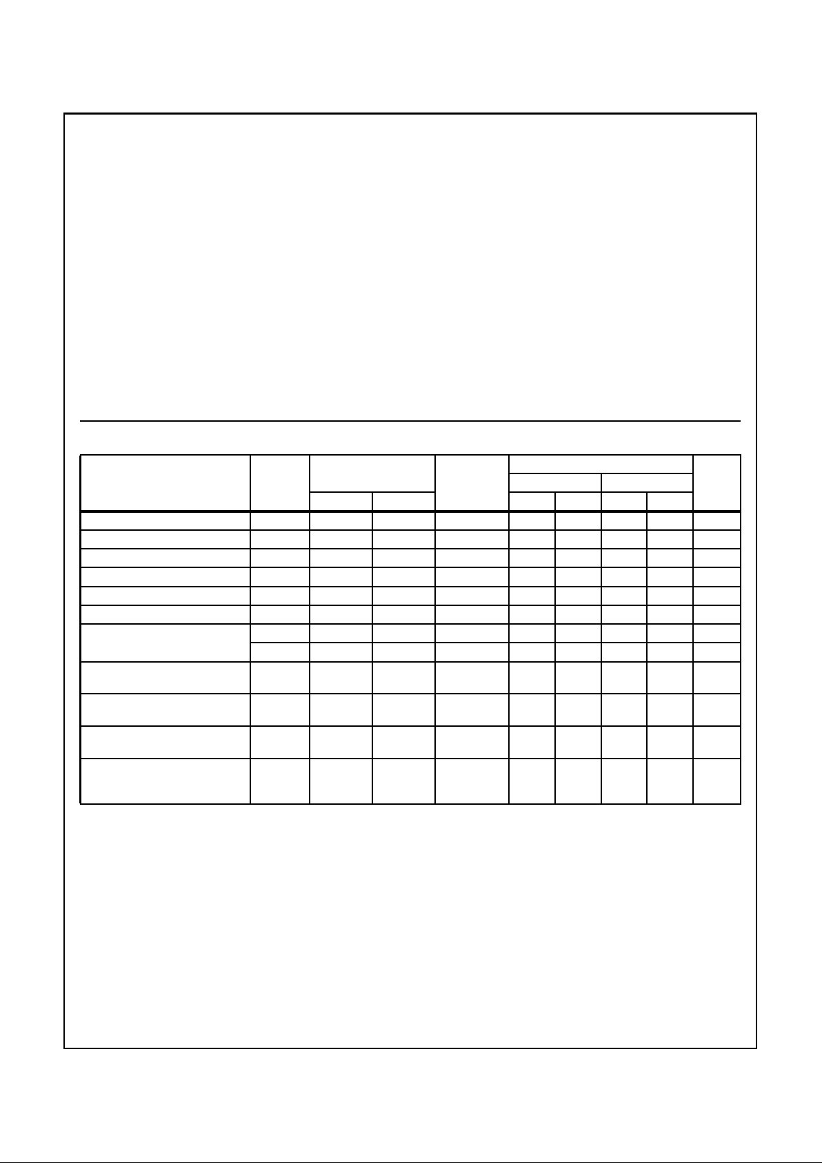
Electrical Specifications Commercial Temperature Range 0
o
C to 70oC, VCC Max = 5.25V, VCC Min = 4.75V (Note 5)
PARAMETER SYMBOL
TEST CONDITIONS
VCC (V)
AMBIENT TEMPERATURE (TA)
UNITS
25oC0
o
C TO 70oC
VI (V) IO (mA) MIN MAX MIN MAX
High Level Input Voltage V
IH
4.75 to 5.25 2 - 2 - V
Low Level Input Voltage V
IL
4.75 to 5.25 - 0.8 - 0.8 V
High Level Output Voltage V
OH
VIH or V
IL
-15 Min 2.4 - 2.4 - V
Low Level Output Voltage V
OL
VIH or V
IL
48 Min - 0.55 - 0.55 V
High Level Input Current I
IH
V
CC
Max - 0.1 - 1 µA
Low Level Input Current I
IL
GND Max - -0.1 - -1 µA
Three State Leakage Current I
OZH
V
CC
Max - 0.5 - 10 µA
I
OZL
GND Max - -0.5 - -10 µA
Input Clamp Voltage V
IK
VCC or
GND
-18 Min - -1.2 - -1.2 V
Short Circuit Output Current
(Note 3)
I
OS
VO=0V
CC
or GND
Max -60 - -60 - mA
Quiescent Supply Current,
MSI
I
CC
VCC or
GND
0 Max - 8 - 80 µA
Additional Quiescent Supply
Current per Input Pin
TTL Inputs High, 1 Unit Load
∆I
CC
3.4V
(Note 4)
Max - 1.6 - 1.6 mA
NOTES:
3. Not more than one output should be shorted at one time. Test duration should not exceed 100ms.
4. Inputs that are not measured are at VCC or GND.
5. FCT Input Loading: All inputs are 1 unit load. Unit load is ∆ICC limit specified in Static Characteristics Chart, e.g., 1.6mA Max. at 70oC.
CD74FCT273

4
Switching Specifications Over Operating Range FCT Series t
r
, tf= 2.5ns, CL = 50pF, RL (Figure 4) (Note 6)
PARAMETER SYMBOL VCC (V)
25oC0oC TO 70oC
UNITSTYP MIN MAX
Propagation Delays
CP to Qn t
PLH
, t
PHL
57213ns
MR to Qn t
PLH
, t
PHL
58213ns
Power Dissipation Capacitance C
PD
(Note 7)
-36- - pF
Input Capacitance C
I
---10pF
NOTES:
6. 5V: Min is at 5.25V for 0oC to 70oC, Max is at 4.75V for 0oC to 70oC, Typ is at 5V.
7. CPD, measured per flip-flop, is used to determine the dynamic power consumption.
PD (per package) = VCC ICC + Σ(V
CC
2
fI CPD + V
O
2
fO CL + VCC∆ICC D) where:
VCC = supply voltage
∆ICC = flow through current x unit load
CL = output load capacitance
D = duty cycle of input high
fO = output frequency
fI = input frequency
Prerequisite for Switching (Note 8)
PARAMETER SYMBOL VCC (V)
25oC0
o
C TO 70oC
UNITSTYP MIN MAX
Data to CP Setup Time t
SU
5-3-ns
Hold Time t
H
5-2-ns
Removal Time, MR to CP t
REM
5-4-ns
MR Pulse Width t
W
5-7-ns
CP Pulse Width t
W
5-7-ns
CP Frequency f
MAX
5 - 70 - MHz
NOTE:
8. 5V: Minimum is at 4.75V for 0oC to 70oC, Typical is at 5V.
CD74FCT273

5
CD74FCT273
Test Circuits and Waveforms
NOTE:
9. Pulse Generator for All Pulses: Rate ≤ 1.0MHz; Z
OUT
≤ 50Ω;
tf, tr≤ 2.5ns.
FIGURE 1. TEST CIRCUIT
FIGURE 2. SETUP, HOLD, AND RELEASE TIMING FIGURE 3. PULSE WIDTH
FIGURE 4. ENABLE AND DISABLE TIMING FIGURE 5. PROPAGATION DELAY
3V
0
DUT
PULSE Z
O
GEN
7V
500Ω
50pF
500Ω
V
CC
R
T
RT = Z
O
V
0
C
L
R
L
R
L
V
I
tr, tf = 2.5ns
(NOTE 9)
SWITCH POSITION
TEST SWITCH
t
PLZ
, t
PZL
, Open Drain Closed
t
PHZ
, t
PZH
, t
PLH
, t
PHL
Open
DEFINITIONS:
CL = Load capacitance, includes jig and probe
capacitance.
RT= Termination resistance, should be equal to Z
OUT
of
the Pulse Generator.
VIN = 0V to 3V.
Input: tr=tf= 2.5ns (10% to 90%), unless otherwise specified
ASYNCHRONOUS CONTROL
t
H
t
SH
3V
1.5V
0V
3V
1.5V
0V
3V
1.5V
0V
3V
1.5V
0V
t
H
t
SH
PRESET CLEAR
CLOCK ENABLE
ETC.
SYNCHRONOUS CONTROL
t
REM
DAT A
INPUT
TIMING
INPUT
t
W
LOW-HIGH-LOW
PULSE
HIGH-LOW-HIGH
PULSE
1.5V
1.5V
3V
1.5V
0V
CONTROL INPUT
OUTPUT
NORMALLY LOW
OUTPUT
NORMALLY HIGH
SWITCH
OPEN
t
PZL
3.5V
1.5V
1.5V
0V
t
PLZ
t
PHZ
t
PZH
0V
3.5V
0.3V
0.3V
V
OL
V
OH
SWITCH
CLOSED
ENABLE DISABLE
1.5V
3V
0V
1.5V
3V
0V
t
PLH
SAME PHASE
INPUT TRANSITION
t
PHL
t
PLH
t
PHL
OPPOSITE PHASE
INPUT TRANSITION
OUTPUT
1.5V
V
OH
V
OL

6
NOTES:
10. V
OLP
is measured with respect to a ground reference near the output under test. V
OHV
is measured with respect to VOH.
11. Input pulses have the following characteristics:
PRR≤ 1MHz, tr = 2.5ns, tf = 2.5ns, skew 1ns.
12. R.F. fixture with 700MHz design rules required. IC should be soldered into test board and bypassed with 0.1µF capacitor. Scope and
probes require 700MHz bandwidth.
FIGURE 6. SIMUL TANEOUS SWITCHING TRANSIENT WAVEFORMS
Test Circuits and Waveforms
(Continued)
OTHER
OUTPUTS
OUTPUT
UNDER
TEST
V
OH
V
OL
V
OH
V
OHV
V
OLP
V
OL

IMPORTANT NOTICE
T exas Instruments and its subsidiaries (TI) reserve the right to make changes to their products or to discontinue
any product or service without notice, and advise customers to obtain the latest version of relevant information
to verify, before placing orders, that information being relied on is current and complete. All products are sold
subject to the terms and conditions of sale supplied at the time of order acknowledgement, including those
pertaining to warranty, patent infringement, and limitation of liability.
TI warrants performance of its semiconductor products to the specifications applicable at the time of sale in
accordance with TI’s standard warranty. Testing and other quality control techniques are utilized to the extent
TI deems necessary to support this warranty. Specific testing of all parameters of each device is not necessarily
performed, except those mandated by government requirements.
CERT AIN APPLICATIONS USING SEMICONDUCTOR PRODUCTS MAY INVOLVE POTENTIAL RISKS OF
DEATH, PERSONAL INJURY, OR SEVERE PROPERTY OR ENVIRONMENTAL DAMAGE (“CRITICAL
APPLICATIONS”). TI SEMICONDUCTOR PRODUCTS ARE NOT DESIGNED, AUTHORIZED, OR
WARRANTED TO BE SUITABLE FOR USE IN LIFE-SUPPORT DEVICES OR SYSTEMS OR OTHER
CRITICAL APPLICATIONS. INCLUSION OF TI PRODUCTS IN SUCH APPLICA TIONS IS UNDERSTOOD T O
BE FULLY AT THE CUSTOMER’S RISK.
In order to minimize risks associated with the customer’s applications, adequate design and operating
safeguards must be provided by the customer to minimize inherent or procedural hazards.
TI assumes no liability for applications assistance or customer product design. TI does not warrant or represent
that any license, either express or implied, is granted under any patent right, copyright, mask work right, or other
intellectual property right of TI covering or relating to any combination, machine, or process in which such
semiconductor products or services might be or are used. TI’s publication of information regarding any third
party’s products or services does not constitute TI’s approval, warranty or endorsement thereof.
Copyright 1998, Texas Instruments Incorporated
 Loading...