

D
Digital Design Avoids Analog
Compensation Errors
D
Easily Cascadable for Hlgher Order Loops
D
Useful Frequency Range
– DC to 110 MHz Typical (K CLK)
– DC to 70 MHz Typical (I/D CLK)
D
Dynamically Variable Bandwidth
D
Very Narrow Bandwidth Attainable
D
Power-On Reset
D
Output Capability
– Standand: XORPD OUT, ECPD OUT
– Bus Drlver: I/D OUT
D
SCR Latch-Up-Resistant CMOS Process
and Circuit Design
D
Speed of Bipolar FAST/AS/S with
Significantly Reduced Power Consumption
D
Balanced Propagation Delays
D
ESD Protectlon Exceeds 2000 V per
MIL-STD-883, Method 3015
D
Packaged in Small-Outline Integrated
Circuit Package
description
CD74ACT297
DIGITAL PHASE-LOCKED LOOP
SCHS297A – AUGUST 1998 – REVISED SEPTEMBER 1999
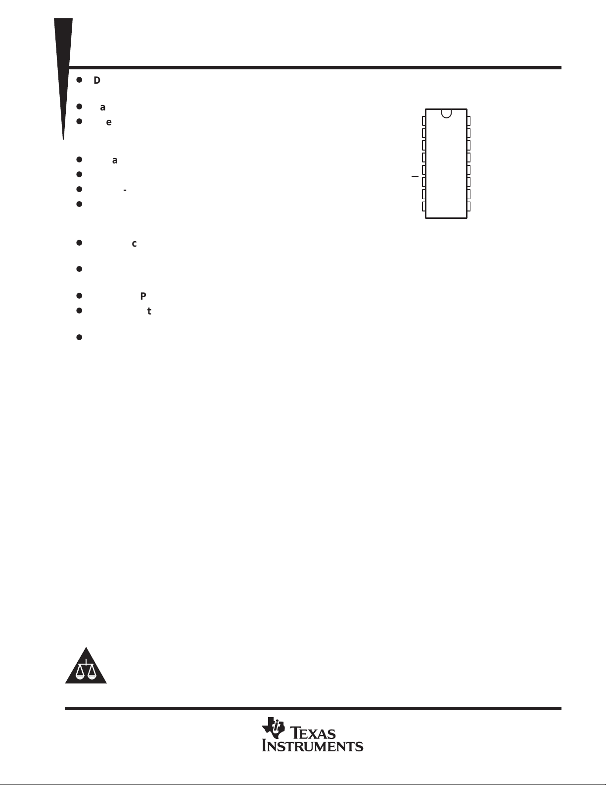
M PACKAGE
(TOP VIEW)
ENCTR
K CLK
I/D CLK
D/U
I/D OUT
GND
B
1
A
2
3
4
5
6
7
8
V
16
CC
C
15
D
14
φA2
13
ECPD OUT
12
XORPD OUT
11
φB
10
9
φA1
The CD74ACT297 device is designed to provide a simple, cost-effective solution to high-accuracy, digital,
phase-locked-loop applications. These devices contain all the necessary circuits, with the exception of the
divide-by-N counter, to build first-order phase-locked loops as described in Figure 1.
Both exclusive-OR (XORPD) and edge-controlled (ECPD) phase detectors are provided for maximum flexibility .
Proper partitioning of the loop function, with many of the building blocks external to the package, makes it easy
for the designer to incorporate ripple cancellation or to cascade to higher order phase-locked loops.
The length of the up/down K counter is digitally programmable according to the K-counter function table. With
A, B, C, and D all low, the K counter is disabled. With A high and B, C, and D low, the K counter is only three
stages long, which widens the bandwidth or capture range and shortens the lock time of the loop. When A, B,
C, and D are programmed high, the K counter becomes 17 stages long, which narrows the bandwidth or capture
range and lengthens the lock time. Real-time control of loop bandwidth by manipulating the A-through-D inputs
can maximize the overall performance of the digital phase-locked loop.
This device performs the classic first-order phase-locked-loop function without using analog components. The
accuracy of the digital phase-locked loop (DPLL) is not affected by VCC and temperature variations, but depends
solely on accuracies of the K clock, I/D clock, and loop propagation delays. The I/D clock frequency and the
divide-by-N modulos determine the center frequency of the DPLL. The center frequency is defined by the
relationship f
= I/D clock/2N (Hz).
c
The CD74ACT297 is characterized for operation from –40°C to 85°C.
Please be aware that an important notice concerning availability, standard warranty, and use in critical applications of
Texas Instruments semiconductor products and disclaimers thereto appears at the end of this data sheet.
TI is a trademark of Texas Instruments Incorporated.
FAST is a trademark of Fairchild Semiconductor.
PRODUCTION DATA information is current as of publication date.
Products conform to specifications per the terms of Texas Instruments
standard warranty. Production processing does not necessarily include
testing of all parameters.
POST OFFICE BOX 655303 • DALLAS, TEXAS 75265
Copyright 1999, Texas Instruments Incorporated
1

CD74ACT297
DIGITAL PHASE-LOCKED LOOP
SCHS297A – AUGUST 1998 – REVISED SEPTEMBER 1999
Modulo Controls
DC B A
14 15 1 2
K CLK
D/U
ENCTR
I/D CLK
φA1
φB
φA2
10
13
4
6
3
5
9
Modulo K
Counter
J
K
Increment/Decrement
Circuit
7
I/D OUT
11
XORPD OUT
12
ECPD OUT
Figure 1. Simplifed Block Diagram
2
POST OFFICE BOX 655303 • DALLAS, TEXAS 75265
CD74ACT297
DIGITAL PHASE-LOCKED LOOP
SCHS297A – AUGUST 1998 – REVISED SEPTEMBER 1999
Function Tables
K COUNTER
(DIGITAL CONTROL)
D
L L L L Inhibited
L L L H 2
L L H L 2
L L H H 2
L H L L 2
L H L H 2
L H H L 2
L H H H 2
H L L L 2
H L L H 2
H L H L 2
H L H H 21
H H L L 2
H H L H 2
H H H L 2
H H H H 2
C B A MODULO (K)
EXCLUSIVE-OR PHASE DETECTOR
φA1
L L L
L H H
H L H
H H L
φB XORPD OUT
3
4
5
6
7
8
9
10
11
12
3
14
15
16
17
EDGE-CONTROLLED PHASE DETECTOR
φA2
H or L ↓ H
↓ H or L L
H or L ↑ No change
↑ H or L No change
H = steady-state high level
L = steady-state low level
↓ = transition from high to low
↑ = transition from low to high
POST OFFICE BOX 655303 • DALLAS, TEXAS 75265
φB ECPD OUT
3
CD74ACT297
DIGITAL PHASE-LOCKED LOOP
SCHS297A – AUGUST 1998 – REVISED SEPTEMBER 1999
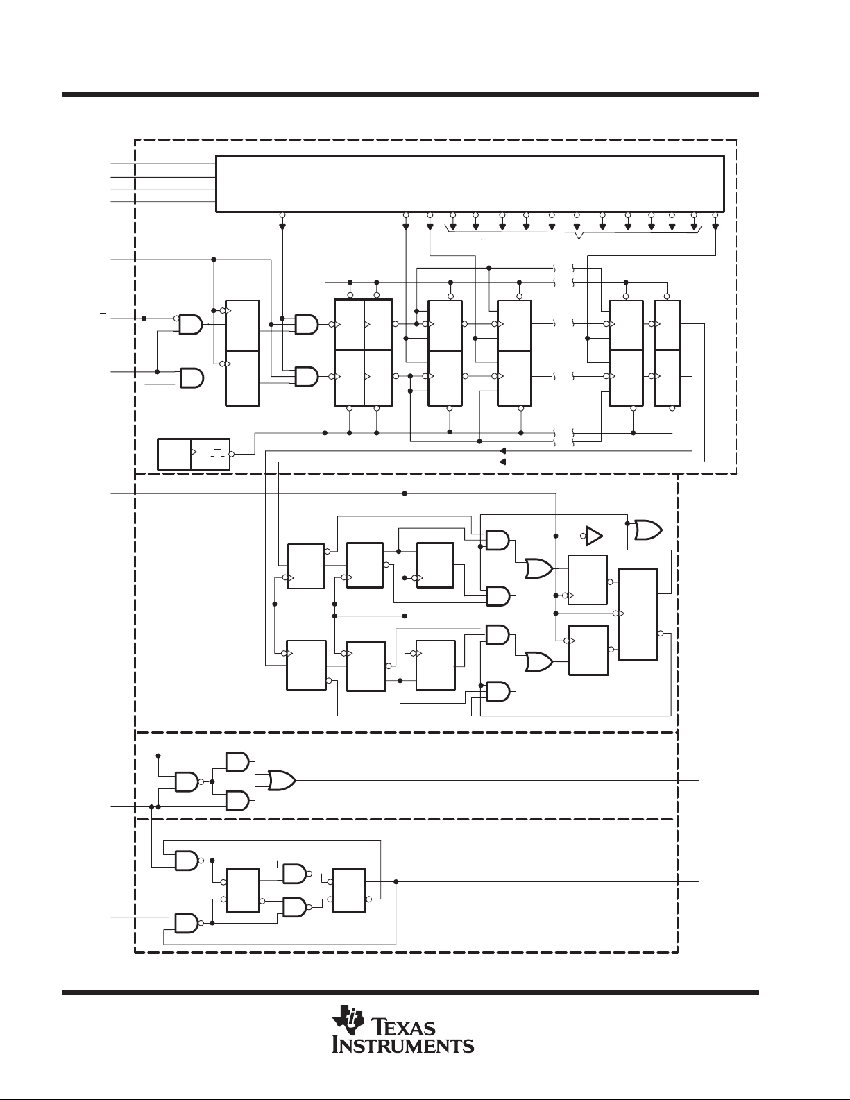
functional block diagram
K CLK
D/U
ENCTR
I/D CLK
2
A
1
B
15
C
14
D
4
6
3
POWER-UP RESET
l = 1
5
1
2
4
8
C20
20D
C20
20D
1
21D
C21
RR
T
T
TT
I/D Circuit
21D
C21
K Counter
X/Y
140
To Mode Controls 12–2 (11 stages not shown)
RR RR
14D
14T
M14
M14
14T
14D
21D
C21
13D
13T
M13
M13
13T
13D
78910111213
21D
C21
4635
1T
1T
RRRRR
Decrement
Increment
21J
C21
T
T
R
21
7
I/D OUT
φA1
φB
φA2
C21
21D
9
10
SS
13
C21
21D
Exclusive-OR Phase Detector
Edge-Controlled Phase Detector
RR
C21
21D
C21
21D
21K
11
XORPD OUT
12
ECPD OUT
4
POST OFFICE BOX 655303 • DALLAS, TEXAS 75265

CD74ACT297
DIGITAL PHASE-LOCKED LOOP
SCHS297A – AUGUST 1998 – REVISED SEPTEMBER 1999
The phase detector generates an error-signal waveform that, at zero phase error, is a 50% duty-cycle square
wave. At the limits of linear operation, the phase-detector output will be either high or low all of the time,
depending on the direction of the phase error (φin – φ
linearly with the input phase error according to the gain kd, which is expressed in terms of phase-detector output
per cycle of phase error. The phase-detector output can be varied between ±1 according to the relation:
). Within these limits, the phase-detector output varies
out
Phase-detector output
The output of the phase detector will be kd φe, where the phase error φe = φin – φ
%high–%low
+
100
out
(1)
.
Exclusive-OR phase detectors (XORPD) and edge-controlled phase detectors (ECPD) are commonly used
digital types. The ECPD is more complex than the XORPD logic function, but can be described generally as
a circuit that changes states on one of the transitions of its inputs. For an XORPD, kd is 4 because its output
remains high (PD output = 1) for a phase error of 1/4 cycle. Similarly , for the ECPD, kd is 2 because its output
remains high for a phase error of 1/2 cycle. The type of phase detector will determine the zero-phase-error point,
i.e., the phase separation of the phase-detector inputs for φ
defined to be zero. For the basic DPLL system of
e
Figure 2, φe = 0 when the phase-detector output is a square wave. The XORPD inputs are 1/4 cycle out of phase
for zero phase error. For the ECPD, φe = 0 when the inputs are 1/2 cycle out of phase.
f
out
fin, φ
fin, φ
, φ
Mf
out
c
in
in
K CLK
D/U
XORPD OUT
φA1
φB
Divide-By-K
Counter
Divide-By-N
Counter
I/D OUT
Carry
Borrow
I/D Circuit
I/D CLK
2 Nf
c
Figure 2. DPLL Using Exclusive-OR Phase Detection
The phase-detector output controls the up/down input to the K counter. The counter is clocked by input
frequency Mfc, which is a multiple M of the loop center frequency fc. When the K counter recycles up, it generates
a carry pulse. Recycling while counting down generates a borrow pulse. If the carry and borrow outputs are
conceptually combined into one output that is positive for a carry and negative for a borrow, and if the K counter
is considered as a frequency divider with the ratio Mf
/K, the output of the K counter will equal the input frequency
c
multiplied by the division ratio. Thus, the output from the K counter is (kdφeMfc)K.
The carry and borrow pulses go to the increment/decrement (I/D) circuit, which, in the absence of any carry or
borrow pulse, has an output that is one half of the input clock (I/D CLK). The input clock is just a multiple, 2N,
of the loop center frequency. In response to a carry or borrow pulse, the I/D circuit will either add or delete a
pulse at I/D OUT. Thus, the output of the I/D circuit will be Nf
4 (kdφeMfc)/2K.
c
The output of the N counter (or the output of the phase-locked loop) is:
fo+
fc)
(kdfeMfc)ń2KN
(2)
When this result is compared to the equation for a first-order analog phase-locked loop, the digital equivalent
of the gain of the VCO is just Mfc/2KN or fc/K for M = 2N.
Thus, the simple first-order phase-locked loop with an adjustable K counter is the equivalent of an analog
phase-locked loop with a programmable VCO gain.
POST OFFICE BOX 655303 • DALLAS, TEXAS 75265
5

CD74ACT297
DIGITAL PHASE-LOCKED LOOP
SCHS297A – AUGUST 1998 – REVISED SEPTEMBER 1999
f
out
, φ
fin, φ
Mf
out
in
c
K CLK
D/U
ENCTR
XORPD OUT
φA1
φB
φA2
Divide-By-N
J
ECPD
K
Counter
Divide-By-K
Counter
I/D OUT
Carry
Borrow
I/D Circuit
I/D CLK
2 Nf
c
Figure 3. DPLL Using Both Phase Detectors in a Ripple-Cancellation Scheme
absolute maximum ratings over recommended operating free-air temperature range (unless
otherwise noted)
Supply voltage range, VCC –0.5 V to 6 V. . . . . . . . . . . . . . . . . . . . . . . . . . . . . . . . . . . . . . . . . . . . . . . . . . . . . . . . . .
DC input diode current, I
DC input diode current, I
DC output source or sink current per output pin, I
Continuous current through V
Package thermal impedance,θJA (see Note 2) 73°C/W. . . . . . . . . . . . . . . . . . . . . . . . . . . . . . . . . . . . . . . . . . . . . .
Storage temperature range, T
†
Stresses beyond those listed under “absolute maximum ratings” may cause permanent damage to the device. These are stress ratings only, and
functional operation of the device at these or any other conditions beyond those indicated under “recommended operating conditions” is not
implied. Exposure to absolute-maximum-rated conditions for extended periods may affect device reliability.
NOTES: 1. For up to four outputs per device, add ±25 mA for each additional output.
2. The package thermal impedance is calculated in accordance with JESD 51.
†
(VI < –0.5 V or VI > V
IK
(VO < –0.5 V or VO > V
OK
or GND (Note 1) ±100 mA. . . . . . . . . . . . . . . . . . . . . . . . . . . . . . . . . . . . . . . . . .
CC
–65°C to 150°C. . . . . . . . . . . . . . . . . . . . . . . . . . . . . . . . . . . . . . . . . . . . . . . . . . .
stg
+ 0.5 V) ±20 mA. . . . . . . . . . . . . . . . . . . . . . . . . . . . . . . . .
CC
+ 0.5 V) ±50 mA. . . . . . . . . . . . . . . . . . . . . . . . . . . . . .
CC
(VO > –0.5 V or VO < V
O
+ 0.5 V) ±50 mA. . . . . . . . . .
CC
recommended operating conditions
MIN MAX UNIT
V
V
V
V
V
dt/dv Input rise and fall slew rate 10 ns
T
6
Supply voltage 4.5 5.5 V
CC
High-level input voltage 2 V
IH
Low-level input voltage 0.8 V
IL
Input voltage 0 V
I
Output voltage 0 V
O
Operating free-air temperature range –40 85 °C
A
POST OFFICE BOX 655303 • DALLAS, TEXAS 75265
CC
CC
V
V

PARAMETER
TEST CONDITIONS
V
MIN
MAX
UNIT
CD74ACT297
DIGITAL PHASE-LOCKED LOOP
SCHS297A – AUGUST 1998 – REVISED SEPTEMBER 1999
electrical characteristics over recommended operating free-air temperature range (unless
otherwise noted)
CC
IO = –50 µA 4.5 V 4.4 4.4
V
OH
V
OL
I
I
ICC (MSI) VI = VCC or GND 5.5 V 8 80
ICC (SSI/FF) VI = VCC or GND 5.5 V 4 40
D
I
CC
†
T est one output at a time for a 1-second maximum duration. Measurement is made by forcing current and measuring voltage to minimize power
dissipation. Test verifies a minimum 50-Ω transmission-line drive capability at 85°C.
VI = VIH or V
VI =VIH or V
VI = VCC or GND 5.5 V ±0.1 ±1
VI = VCC –2.1 V 4.5 V to 5.5 V 2.4 2.8 mA
IL
IL
IO = –24 mA 4.5 V 3.94 3.8
IO = –75 mA 5.5 V 3.85
IO = 50 µA 4.5 V 0.1 0.1
IO = 24 mA 4.5 V 0.36 0.44
IO = 75 mA
†
ACT Input Load Table
5.5 V 1.65
TA = 25°C
MIN MAX
V
V
m
A
m
A
m
A
INPUT
ENCTR, D/U 0.1
A, B, C, D, K CLK, φA2 0.2
I/O CLK, φA1, φB 0.5
NOTE: Unit Load is ∆ICC limit specified in
electrical characteristics table (e.g.,
2.4 mA at 25°C).
UNIT LOAD
POST OFFICE BOX 655303 • DALLAS, TEXAS 75265
7

CD74ACT297
PARAMETER
MIN
MAX
UNIT
f
Clock frequenc
MH
twPulse duration
ns
t
Set
CLK↑
ns
t
Hold ti
CLK↑
ns
DIGITAL PHASE-LOCKED LOOP
SCHS297A – AUGUST 1998 – REVISED SEPTEMBER 1999
timing requirements over recommended ranges of supply voltage and operating free-air
temperature (unless otherwise noted)
TA = 25°C
MIN MAX
clock
su
h
y
up time before K
me after K
Carry Pulse
(Internal Signal)
Borrrow Pulse
(Internal Signal)
K CLK 55 45
I/D CLK
K CLK 6 8
I/D CLK 7 9
D/U 13 17
ENCTR 12 16
D/U 3 7
ENCTR 2 6
40 35
z
I/D CLK
I/D OUT
φB
φA2
ECPD OUT
92CS-40449
Figure 4. I/D OUT In Lock Condition
92CS-40450
Figure 5. Edge-Controlled Phase-Comparator Waveforms
8
POST OFFICE BOX 655303 • DALLAS, TEXAS 75265

CD74ACT297
DIGITAL PHASE-LOCKED LOOP
SCHS297A – AUGUST 1998 – REVISED SEPTEMBER 1999
φB
φA1
XORPD OUT
92CS-40451
Figure 6. Exclusive-OR Phase-Detector Waveforms
1/F max
t
I/D CLK
I/D OUT
t
PHL
t
TLH
90%
10%
1.5 V
w
50% V
CC
1.5 V
50% V
t
PHL
t
THL
CC
92CS-40452
3 V
0 V
≈V
V
CC
OL
Figure 7. Waveforms Showing Clock (ID CLK) to Output (ID OUT) Propagation Delays,
Clock Pulse Duration, and Maximum Clock Pulse Frequency
3 V
φB
φA1
XORPD OUT
1.5 V
t
PHL
50% V
t
PLH
1.5 V
CC
50% V
1.5 V
CC
t
PLH
50% V
CC
1.5 V
50% V
CC
92CS-43151
t
PHL
0 V
3 V
0 V
≈V
V
CC
OL
Figure 8. Waveforms Showing Phase Input (φB, φA2) to Output (XORPD OUT) Propagation Delays
POST OFFICE BOX 655303 • DALLAS, TEXAS 75265
9

CD74ACT297
PARAMETER
MIN
MAX
UNIT
f
I/D OUT
MH
I/D CLK
I/D OUT
ns
A
XORPD OUT
ns
φB
XORPD OUT
ns
DIGITAL PHASE-LOCKED LOOP
SCHS297A – AUGUST 1998 – REVISED SEPTEMBER 1999
φB
φA2
ECPD OUT
t
PHL
1.5 V
1.5 V
50% V
CC
1.5 V
50% V
t
PLH
CC
3 V
0 V
3 V
0 V
≈V
CC
V
OL
92CS-43152
Figure 9. Waveforms Showing Phase Input (φB, φA2) to Output (ECPD OUT) Propagation Delays
t
H
D/U
ENCTR
t
su
K CLK
NOTE A: Shaded areas indicate when the input is permitted to change for predictable output performance.
1.5 V
1.5 V 1.5 V 1.5 V
1.5 V 1.5 V 1.5 V
t
w
1/f
max
t
H
t
su
92CS-40453
3 V
0 V
3 V
0 V
Figure 10. Waveforms Showing Clock (K CLK) Pulse Duration and Maximum Clock Pulse Frequency,
and Inputs (D/U, ENCTR) to Clock (K CLK) Setup and Hold Times.
switching characteristics over recommended operating free-air temperature range, CL = 50 pF,
(unless otherwise noted)
TA = 25°C
MIN TYP MAX
55 45
40 35
19 24
19 24
24 30 ns
17 22
17 22
17 22
17 22
24 30 ns
z
max
t
PLH
t
PHL
t
PHL
t
PLH
t
PHL
t
PLH
t
PHL
t
PLH
FROM TO
(INPUT) (OUTPUT)
K CLK
I/D CLK
φA
φ
2
1
φB
ECPD OUT
ECPD OUT
10
POST OFFICE BOX 655303 • DALLAS, TEXAS 75265

From Output
Under Test
CL = 50 pF
(see Note A)
DIGITAL PHASE-LOCKED LOOP
SCHS297A – AUGUST 1998 – REVISED SEPTEMBER 1999
PARAMETER MEASUREMENT INFORMATION
2 × V
500 Ω
500 Ω
S1
CC
Open
GND
TEST S1
t
PLH/tPHL
t
PLZ/tPZL
t
PHZ/tPZH
CD74ACT297
Open
2 × V
CC
GND
LOAD CIRCUIT
t
w
90% 90%
Input
INPUT RISE AND FALL TIMES AND PULSE DURATION
Input
In-Phase
Output
Out-of-Phase
Output
1.5 V 1.5 V
t
r
VOLTAGE WAVEFORMS
1.5 V 1.5 V
t
PLH
50% V
CC
t
PHL
50% V
CC
VOLTAGE WAVEFORMS
PROPAGATION DELAY TIMES
10%10%
50% V
t
f
t
PHL
50% V
t
PLH
3 V
0 V
CC
CC
3 V
0 V
V
V
V
V
OH
OL
OH
OL
Timing Input
Data Input
Output
Control
(low-level
enabling)
Output
Waveform 1
S1 at 2 × V
(see Note B)
Output
Waveform 2
S1 at GND
(see Note B)
CC
1.5 V
t
su
1.5 V
VOLTAGE WAVEFORMS
SETUP AND HOLD TIMES
1.5 V
t
PZL
50% V
CC
t
PZH
50% V
CC
VOLTAGE WAVEFORMS
ENABLE AND DISABLE TIMES
t
h
1.5 V
1.5 V
t
PLZ
20% V
t
PHZ
80% V
CC
CC
3 V
0 V
3 V
0 V
3 V
0 V
[
V
V
[
V
OL
OH
0 V
CC
NOTES: A. CL includes probe and jig capacitance.
B. Waveform 1 is for an output with internal conditions such that the output is low except when disabled by the output control.
Waveform 2 is for an output with internal conditions such that the output is high except when disabled by the output control.
C. All input pulses are supplied by generators having the following characteristics: PRR ≤ 1 MHz, ZO = 50 Ω, tr = 3 ns, tf = 3 ns.
D. The outputs are measured one at a time with one input transition per measurement.
Figure 11. Load Circuit and Voltage Waveforms
POST OFFICE BOX 655303 • DALLAS, TEXAS 75265
11

IMPORTANT NOTICE
T exas Instruments and its subsidiaries (TI) reserve the right to make changes to their products or to discontinue
any product or service without notice, and advise customers to obtain the latest version of relevant information
to verify, before placing orders, that information being relied on is current and complete. All products are sold
subject to the terms and conditions of sale supplied at the time of order acknowledgement, including those
pertaining to warranty, patent infringement, and limitation of liability.
TI warrants performance of its semiconductor products to the specifications applicable at the time of sale in
accordance with TI’s standard warranty. Testing and other quality control techniques are utilized to the extent
TI deems necessary to support this warranty . Specific testing of all parameters of each device is not necessarily
performed, except those mandated by government requirements.
CERTAIN APPLICA TIONS USING SEMICONDUCT OR PRODUCTS MAY INVOLVE POTENTIAL RISKS OF
DEATH, PERSONAL INJURY, OR SEVERE PROPERTY OR ENVIRONMENTAL DAMAGE (“CRITICAL
APPLICATIONS”). TI SEMICONDUCTOR PRODUCTS ARE NOT DESIGNED, AUTHORIZED, OR
WARRANTED TO BE SUITABLE FOR USE IN LIFE-SUPPORT DEVICES OR SYSTEMS OR OTHER
CRITICAL APPLICA TIONS. INCLUSION OF TI PRODUCTS IN SUCH APPLICATIONS IS UNDERST OOD TO
BE FULLY AT THE CUSTOMER’S RISK.
In order to minimize risks associated with the customer’s applications, adequate design and operating
safeguards must be provided by the customer to minimize inherent or procedural hazards.
TI assumes no liability for applications assistance or customer product design. TI does not warrant or represent
that any license, either express or implied, is granted under any patent right, copyright, mask work right, or other
intellectual property right of TI covering or relating to any combination, machine, or process in which such
semiconductor products or services might be or are used. TI’s publication of information regarding any third
party’s products or services does not constitute TI’s approval, warranty or endorsement thereof.
Copyright 1999, Texas Instruments Incorporated
 Loading...